EP0410374A2 - Supraleitende Mehrlagen-Schaltung und Verfahren zu deren Herstellung - Google Patents
Supraleitende Mehrlagen-Schaltung und Verfahren zu deren Herstellung Download PDFInfo
- Publication number
- EP0410374A2 EP0410374A2 EP90114152A EP90114152A EP0410374A2 EP 0410374 A2 EP0410374 A2 EP 0410374A2 EP 90114152 A EP90114152 A EP 90114152A EP 90114152 A EP90114152 A EP 90114152A EP 0410374 A2 EP0410374 A2 EP 0410374A2
- Authority
- EP
- European Patent Office
- Prior art keywords
- circuit
- superconductive
- thin film
- multilayer circuit
- layer
- Prior art date
- Legal status (The legal status is an assumption and is not a legal conclusion. Google has not performed a legal analysis and makes no representation as to the accuracy of the status listed.)
- Granted
Links
Images

Classifications
-
- H—ELECTRICITY
- H10—SEMICONDUCTOR DEVICES; ELECTRIC SOLID-STATE DEVICES NOT OTHERWISE PROVIDED FOR
- H10N—ELECTRIC SOLID-STATE DEVICES NOT OTHERWISE PROVIDED FOR
- H10N60/00—Superconducting devices
- H10N60/01—Manufacture or treatment
- H10N60/0268—Manufacture or treatment of devices comprising copper oxide
- H10N60/0661—Processes performed after copper oxide formation, e.g. patterning
-
- H—ELECTRICITY
- H10—SEMICONDUCTOR DEVICES; ELECTRIC SOLID-STATE DEVICES NOT OTHERWISE PROVIDED FOR
- H10N—ELECTRIC SOLID-STATE DEVICES NOT OTHERWISE PROVIDED FOR
- H10N60/00—Superconducting devices
- H10N60/01—Manufacture or treatment
- H10N60/0884—Treatment of superconductor layers by irradiation, e.g. ion-beam, electron-beam, laser beam or X-rays
-
- H—ELECTRICITY
- H10—SEMICONDUCTOR DEVICES; ELECTRIC SOLID-STATE DEVICES NOT OTHERWISE PROVIDED FOR
- H10N—ELECTRIC SOLID-STATE DEVICES NOT OTHERWISE PROVIDED FOR
- H10N60/00—Superconducting devices
- H10N60/80—Constructional details
- H10N60/85—Superconducting active materials
- H10N60/855—Ceramic superconductors
- H10N60/857—Ceramic superconductors comprising copper oxide
- H10N60/858—Ceramic superconductors comprising copper oxide having multilayered structures, e.g. superlattices
-
- Y—GENERAL TAGGING OF NEW TECHNOLOGICAL DEVELOPMENTS; GENERAL TAGGING OF CROSS-SECTIONAL TECHNOLOGIES SPANNING OVER SEVERAL SECTIONS OF THE IPC; TECHNICAL SUBJECTS COVERED BY FORMER USPC CROSS-REFERENCE ART COLLECTIONS [XRACs] AND DIGESTS
- Y10—TECHNICAL SUBJECTS COVERED BY FORMER USPC
- Y10S—TECHNICAL SUBJECTS COVERED BY FORMER USPC CROSS-REFERENCE ART COLLECTIONS [XRACs] AND DIGESTS
- Y10S505/00—Superconductor technology: apparatus, material, process
- Y10S505/70—High TC, above 30 k, superconducting device, article, or structured stock
- Y10S505/701—Coated or thin film device, i.e. active or passive
- Y10S505/702—Josephson junction present
-
- Y—GENERAL TAGGING OF NEW TECHNOLOGICAL DEVELOPMENTS; GENERAL TAGGING OF CROSS-SECTIONAL TECHNOLOGIES SPANNING OVER SEVERAL SECTIONS OF THE IPC; TECHNICAL SUBJECTS COVERED BY FORMER USPC CROSS-REFERENCE ART COLLECTIONS [XRACs] AND DIGESTS
- Y10—TECHNICAL SUBJECTS COVERED BY FORMER USPC
- Y10S—TECHNICAL SUBJECTS COVERED BY FORMER USPC CROSS-REFERENCE ART COLLECTIONS [XRACs] AND DIGESTS
- Y10S505/00—Superconductor technology: apparatus, material, process
- Y10S505/70—High TC, above 30 k, superconducting device, article, or structured stock
- Y10S505/701—Coated or thin film device, i.e. active or passive
- Y10S505/703—Microelectronic device with superconducting conduction line
-
- Y—GENERAL TAGGING OF NEW TECHNOLOGICAL DEVELOPMENTS; GENERAL TAGGING OF CROSS-SECTIONAL TECHNOLOGIES SPANNING OVER SEVERAL SECTIONS OF THE IPC; TECHNICAL SUBJECTS COVERED BY FORMER USPC CROSS-REFERENCE ART COLLECTIONS [XRACs] AND DIGESTS
- Y10—TECHNICAL SUBJECTS COVERED BY FORMER USPC
- Y10S—TECHNICAL SUBJECTS COVERED BY FORMER USPC CROSS-REFERENCE ART COLLECTIONS [XRACs] AND DIGESTS
- Y10S505/00—Superconductor technology: apparatus, material, process
- Y10S505/725—Process of making or treating high tc, above 30 k, superconducting shaped material, article, or device
- Y10S505/73—Vacuum treating or coating
- Y10S505/731—Sputter coating
-
- Y—GENERAL TAGGING OF NEW TECHNOLOGICAL DEVELOPMENTS; GENERAL TAGGING OF CROSS-SECTIONAL TECHNOLOGIES SPANNING OVER SEVERAL SECTIONS OF THE IPC; TECHNICAL SUBJECTS COVERED BY FORMER USPC CROSS-REFERENCE ART COLLECTIONS [XRACs] AND DIGESTS
- Y10—TECHNICAL SUBJECTS COVERED BY FORMER USPC
- Y10S—TECHNICAL SUBJECTS COVERED BY FORMER USPC CROSS-REFERENCE ART COLLECTIONS [XRACs] AND DIGESTS
- Y10S505/00—Superconductor technology: apparatus, material, process
- Y10S505/725—Process of making or treating high tc, above 30 k, superconducting shaped material, article, or device
- Y10S505/73—Vacuum treating or coating
- Y10S505/732—Evaporative coating with superconducting material
-
- Y—GENERAL TAGGING OF NEW TECHNOLOGICAL DEVELOPMENTS; GENERAL TAGGING OF CROSS-SECTIONAL TECHNOLOGIES SPANNING OVER SEVERAL SECTIONS OF THE IPC; TECHNICAL SUBJECTS COVERED BY FORMER USPC CROSS-REFERENCE ART COLLECTIONS [XRACs] AND DIGESTS
- Y10—TECHNICAL SUBJECTS COVERED BY FORMER USPC
- Y10S—TECHNICAL SUBJECTS COVERED BY FORMER USPC CROSS-REFERENCE ART COLLECTIONS [XRACs] AND DIGESTS
- Y10S505/00—Superconductor technology: apparatus, material, process
- Y10S505/725—Process of making or treating high tc, above 30 k, superconducting shaped material, article, or device
- Y10S505/742—Annealing
Definitions
- the present invention relates to a multilayer circuit having a conductor made up of a superconductive material, and its manufacturing method.
- multilayer circuits which are used in electronic equipments, are formed by use of normal conductive materials or semiconductor materials.
- the formation of a conductive film, coating of a resist, exposure, and etching are performed.
- a circuit part is formed to be projected.
- the circuit part is formed and an insulating material is embedded in the removed non-circuit part, so that the surface of the circuit is caused to flat, thereby forming a first circuit layer.
- a second circuit layer is formed on the first circuit layer in the same manner as the above. Therefore, if the multilayer circuits are formed by the conventional method, the productivity considerably decreases.
- the superconductive material exhibits a superconductive phenomenon on cooling to a very low temperature, which is less than the critical temperature (hereinafter called Tc), and an electrical resistance becomes zero, thereby a large amount of current can be flowed.
- Tc critical temperature
- the application of the superconductive material to the electronic equipments has been widely studied. Particularly, oxide superconductive materials such as Y-Ba-Cu-O system and Bi-Sr-Ca-Cu-O system, which exhibit the superconductive phenomenon near the temperature of liquid nitrogen, has be recently found out, and the practical use of the oxide superconductive materials has been widely made. In accordance with this situation, the development of the multilayer circuits using oxide superconductive materials has been actively made.
- An object of the present invention is to provide a superconductive circuit having a high Jc value.
- Another object of the present invention is to provide a method for effectively manufacturing a superconductive circuit having a high Jc value.
- a superconductive multilayer circuit comprising a substrate; a first circuit layer formed on the substrate, having a circuit part formed of a superconductive material and a non-circuit part formed of a simulant of the superconductive material; and at least one second circuit layer formed on the first circuit layer, having a circuit part formed of a superconductive material and a non-circuit part formed of a simulant of the superconductive material.
- a method for manufacturing a superconductive multilayer circuit comprising a first thin film forming step for forming a thin film, which comprises a superconductive material or a similar material thereto, on a substrate; a first circuit layer forming step for forming a superconductive circuit by removing a specific component from a predetermined part of the thin film or implanting the component in a predetermined part of the thin film; a second thin film forming step for forming a thin film, which comprises a superconductive material or the simulant thereto, on the first circuit layer; and a second circuit layer forming step for forming a superconductive circuit by removing a specific component from a predetermined part of the thin film or implanting the component in a predetermined part of the thin film.
- a superconductive multilayer circuit having three layers or more can be obtained by repeating the second thin film forming step and the second circuit layer forming step a plurality of times.
- oxide superconductive materials such as Y-Ba-Cu-O system and Bi-Sr-Ca-Cu-O system can be used as superconductive materials.
- a simulant of the superconductive material is a material having the same crystal structure as the superconductive material, and lacking in a part of the constituent elements, or containing the constituent elements excessively.
- the simulant of the superconductive material is a material having the same crystal structure as the superconductive material and containing elements other than the constituent elements.
- the simulant of superconductive material is a material having low Tc as compared with the superconductive material or being non-conductive at a working temperature.
- a substrate forming the superconductive material or the simulant there may be used metals which are non-reactive with the superconductive materials such as Cu, Ni, Fe, Co, Cr, Ag, Au, Pt, Mo, Pb, alloies of these metals such as stainless, Cu-Ni alloy, Fe-Ni alloy, Fe-Ni-Co alloy, Ni-Cr-Fe alloy, Ag-Ni alloy, Cu-Fe alloy, or ceramics such as Al2O3, SiO2, ZrO2, stabilized ZrO2, ThO2, AlN, Si3N4, SiC, TiO2, TiN, MgO, BaZrO3, KTaO3, FeAlO4, BaTiO3.
- metals which are non-reactive with the superconductive materials such as Cu, Ni, Fe, Co, Cr, Ag, Au, Pt, Mo, Pb, alloies of these metals such as stainless, Cu-Ni alloy, Fe-Ni alloy, Fe-Ni-Co alloy, Ni-Cr-Fe alloy, Ag-N
- the orientation of the surface of the film formed of the superconductive material is oriented in a predetermined orientation on the substrate, thereby the formation of the film can be made.
- a vapor phase analyzing method such as a normal sputtering method, a vacuum deposition method, and a CVD method is used.
- a photolithography is normally used, but a method for locally irradiating a focus ion beam can be used.
- a substrate 11 may be formed on a superconductive film 11 having a thickness of 0.1 to 10 ⁇ by a physical vapor deposition (PVD) or sputtering.
- PVD physical vapor deposition
- a resist film 12 which serves as a mask having a specific component due to an ion beam, is formed on a predetermined part of a circuit on the superconductive film 11.
- a photosensitive resin having a base of poly methyl methacrylate (PMMA) may be used as a resist material.
- a non-circuit part of the first superconductive film 11 i.e., an exposed portion where no resist film 12 is formed, thereby a specific component is implanted therein and the resist film 12 is removed.
- a heating process is performed as required, and the non-circuit part formed of the superconductive film 10 is denatured to a simulant 13 of the superconductive material (hereinafter called simulant) having Tc lower than the superconductive material.
- simulant the superconductive material having Tc lower than the superconductive material.
- a second superconductive film 15 is further formed on the first circuit layer 14 in the same manner as the first superconductive film 11.
- a non-circuit part is denatured to a simulant 16 in the same manner as the first circuit layer 14, so that a second circuit layer 17 is formed.
- the specific component is implanted in the non-circuit part by the ion beam and the like to denature the superconductive films 11 and 15 to the simulant 13 and 16, respectively.
- the temperature in dissoiating and discharging oxygen is 700°C or more in the air.
- the temperature is 200 to 300°C if it is in the vacuum. The above-mentioned operations are repeated, thereby a multilayer circuit having three or more layers can be formed.
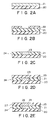
- Figs. 2A to 2E are cross sectional views showing a substrate of the circuit of each step of another embodiment of the present invention.
- a resist film 22 which serves as a mask in which a specific component is implanted in a part other than a predetermined part of a circuit, is formed on the first simulant layer 21.
- the ion beam of oxygen ion is irradiated on the circuit part of the first simulant film 21, i.e., the exposed portion where no resist film 22 is formed, and the oxygen ion is implanted thereon. Thereafter, the resist film 22 is removed. Thereby, as shown in Fig. 2C, the simulant film 21 of the circuit part is denatured to a superconductive material 23, and a first circuit layer 24 having a flat surface is formed.
- a second simulant film 25 which comprises a material having Tc lower than the superconductive material or a non-conductive material at a working temperature, is formed on the first circuit layer 24 in the same manner as the first simulant layer 21.
- the circuit part is denatured to a superconductive material 26, and a second circuit layer 27 is formed.
- a mutual transformation between an oxide superconductive material and the simulant is favorably performed by implanting or discharging atoms of oxygen since it is excellent in workability.
- ion-implantation method using ion beam and the like there may be used a method in which the simulant or the oxide superconductive material is exposed in the oxygen stream activated by plasma of a low temperature or in the vacuum and heated at a predetermined temperature, thereby oxygen atoms are replenished or discharged.
- Tc the relationship between the content of the oxygen atoms and the Tc
- X are 7.0, 0.6, and 6.5
- Tc are 80K or more, less than 77K and 55K or less, respectively.
- the content of the oxygen atoms in the oxide superconductive material slightly changes, the Tc largely changes.
- an element composing the superconductive material other than oxygen is lack or excessively implanted, Tc largely changes. Therefore, it is possible to use a simulant which is obtained by lacking the element composing the superconductive material other than oxygen or excessively implanting the element.
- a method for forming each circuit layer may be changed every layer.
- the first circuit layer may be formed by the method shown in Figs. 1A to 1E
- the second circuit layer may be formed by the method shown in Figs. 2A to 2E.
- a conventional etching method may be used in the formation of the other circuit layers.
- the oxide superconductive material has a strong crystal anisotropy and a short coherence. Due to this, in the oxide superconductive material, current easily flows in a specific crystal orientation (direction of a-b surface). However, if the crystal orientation is not fully consistent with a grain boundary, a current trouble occurs because of a weak bond. This is well-known from Report of Japan Institute of Metal, Vol. 28, No. 10, pp. 980 to 984, October 1987 and Report of Japan Institute of Applied Electromagnetics, Vol. 128, No. 5, pp. 564 to 569, May 1988..
- the material, which constitutes the non-circuit part and the circuit part holds the same or similar crystal structure and has the same crystal orientation as that of the crystal structure, thereby preventing the above-mentioned current trouble.
- the circuit parts 11 and 23 and the non-circuit parts 13 and 21 have the relation to the above-mentioned crystal structure, respectively.
- the circuit parts 15 and 26 of the second circuit layers 17 and 27, which are formed on the first circuit layers 14 and 24 in the similar manner, and the non-circuit parts 16 and 25 are epitaxial-growing. Therefore, the circuit parts 15 and 26 of the the second circuit layer and the circuit parts 11 and 23 of the first circuit layer form a junction having no current trouble, and the crystal orientation is arranged in the direction where current easily flows.
- the third circuit layer forms the structure in which current easily flows similar to the second circuit layer.
- the present invention provides a superconductive multilayer circuit, which can be obtained by forming a thin film, which comprises a superconductive material whose conductivity largely changes if the composition slightly changes and its simulant, on a substrate, implanting a specific component in a predetermined part of the thin film and discharging the component therefrom, and forming the thin film on the circuit parts or the non-curcuit parts.
- the implantation of the specific component and the discharge thereof are performed by an ion implanting and discharging method, thereby fine processing can be performed.
- the crystal orientation of the superconductive material can be arranged in a direction where current easily flows.
- a vapor deposition method such as a sputtering method can be used as a method for forming a thin film, each layer can be formed in such a manner that the crystal orientation is arranged in the same direction.
- a circuit having a flat surface can be obtained, a multilayer circuit can be easily manufactured.
- an epitaxial film having composition of ErBa2Cu3Oy and thickness of 0.5 ⁇ m was formed on a Mgo substrate (100), which had been heated to 650°C, in order to arrange a surface orientation of a surface including ab axes in a conductive direction.
- the magnetron sputtering was performed under the atmosphere of mixed gas of Ar + 20%O2 and on the condition that gas pressure was 80 m Torr and RF output was 100 W.
- the MgO substrate having a first film of ErBa2CU3Oy was provided in a furnace, and oxygen gas was introduced into the furnace, and heated in the oxygen stream at 900°C for 15 minutes. Thereafter, the temperature of the furnace was cooled to 500°C at a speed of 1.5°C/min and MgO substrate was taken out of the furnace.
- a photoresist film was formed on a predetermined part having width of 50 ⁇ m of the circuit of the first film of ErBa2Cu3Oy after heating process. Then, Zn ion of 0.8 ⁇ 1016 ion/cm2 was implanted in the non-circuit part, and the photoresist film was removed therefrom. Thereafter, the substrate is heated at 400°C for 10 minutes and the first film of ErBa2Cu3Oy was annealed, and homogenized. In this manner, a first circuit layer was formed. At this time, Tc of Zn ion-implanted-part was 38K.
- a second film of ErBa2Cu3Oy having thickness of 0.5 ⁇ m was formed on the first circuit layer by a vacuum deposition method.
- Er, Ba, Cu were first put in the different crucibles, respectively and melt in the vacuum of 10 ⁇ 4 Torr and vapored. Then, the vapored Er, Ba, Cu are ionized by a RF excitation coil, which was arranged between the crucible and the substrate, and oxygen gas was sprayed on the substrate which was heated to 590°C.
- a second circuit layer was formed on the second film of ErBa2Cu3Oy by forming a circuit having width of 50 ⁇ m.
- two types of circuits that is, a conductive circuit, which has conductivity with the first circuit, and an independent circuit which has no conductivity with the first circuit.
- circuit part of the first circuit layer and the non-circuit part thereof were checked by an X-ray diffraction.
- the crystal structure of both parts was a rhombic system, and c axis was arranged to be perpendicular to the surface of the substrate.
- a lattice constant of the c axis was 11.68A in the circuit part, and 11.70A in the non-circuit part.
- circuit part of the second circuit layer was checked by the X-ray diffraction.
- c axis was arranged to be perpendicular to the surface of the substrate and the lattice constant of c axis was 11.68A.
- a two-layer circuit having a conductive circuit and an independent circuit was formed in the same manner as Example 1 other than that the thicknesses of first and second films of ErBa2Cu3Oy were 0.3 ⁇ m and that the ion implantation is not used in the second circuit layer. Instead of using the ion implantation, a Fe film having thickness of 0.015 ⁇ m was formed on the non-circuit part of the second ErBa2Cu3Oy, thereafter heating at 450°C.
- circuit part of the first circuit layer and the non-circuit part thereof were checked by the X-ray diffraction.
- c axis was arranged to be perpendicular to the surface of the substrate.
- a lattice constant of the c axis was 11.68A in the circuit part, and 11.73A in the non-circuit part.
- circuit part of the second circuit layer was checked by the X-ray diffraction.
- c axis was arranged to be perpendicular to the surface of the substrate and the lattice constant of c axis was 11.68A in the circuit part, and 11.71A in the non-circuit part.
- a first film of YBa2CU3Oy having thickness of 0.4 ⁇ m was formed on the MgO substrate (100) used in Example 1 by the vapor deposition method (degree of vacuum of 0.5 ⁇ 10 ⁇ 4 Torr).
- a photoresist film was formed on the part other than a predetermined part of the circuit (50 ⁇ m of width). Then, O2 plasma process of the electron cyclotron resonance was performed for 15 minutes as the substrate was heated at 200°C, and oxygen atoms ware incorporated into the predetermined part of the circuit, thereby a first circuit layer was formed.
- a second film of YBa2CU3Oy having thickness of 0.4 ⁇ m was formed on the first circuit layer by the vapor deposition method (degree of vacuum of 0.5 ⁇ 10 ⁇ 4 Torr). Thereafter, a circuit was formed in the same manner as the first circuit layer, thereby a second circuit layer was formed. In this way, a two-layer circuit layer having a conductive circuit and an independent circuit was formed.
- circuit part of the first circuit layer and the non-circuit part thereof were checked by the X-ray diffraction.
- c axis was oriented to be perpendicular to the surface of the substrate.
- a lattice constant of the c axis was 11.67A in the circuit part, and 11.73A in the non-circuit part.
- circuit part of the second circuit layer and the non-circuit part thereof were checked by the X-ray diffraction.
- c axis was oriented to be perpendicular to the surface of the substrate and the lattice constant of c axis was 11.68A in the circuit part and 11.73A in the non-circuit part.
- a first circuit layer was formed in the same manner as Example 1 other than that a Zn thin film having thickness of 0.3 ⁇ m on a non-circuit part by sputtering in place of implanting Zn ion, thereafter heating at 450°C for two hours in the air.
- the obtained first circuit layer was checked by an X-ray diffraction. As a result, it was confirmed that the peak of ErBa2Cu3Oy was only small in the diffraction peak of the circuit part. Also, the peak of ZnO was confirmed in the diffraction peak of the non-circuit part.
- Example 2 Moreover, a second circuit layer was formed on the first circuit layer in the same manner that Example 1.
- Tc and Jc in the conductive circuit and the independent circuit were measured.
- Table 1 shows the results together with the main conditions. Additionally, Jc was measured in liquid nitrogen (77K) by a four terminal method.
- the superconductive multilayer circuit of the present invention exhibited high Tc and Jc.
- Tc of the circuit parts are 83 to 85K.
- Tc of the non-circuit parts are low.
- the part where Zn is implanted and the part, which is oxygen deficiency are 38K and 54K, respectively. Due to this, since these non-circuit parts become insulators at the temperature of liquid nitrogen, no trouble such as a short-circuit is not occurred.
- Jc of the conductive circuit is lower than that of the independent circuit, but a sufficient value as a multilayer circuit. This proves that the first and second circuit layers have the same orientation of surface, and are connected to each other.
- the width of the circuit is 50 ⁇ m.
- the width of the circuit is ⁇ m and a fine pattern is sub ⁇ m order.
Landscapes
- Engineering & Computer Science (AREA)
- Manufacturing & Machinery (AREA)
- Physics & Mathematics (AREA)
- Optics & Photonics (AREA)
- Chemical & Material Sciences (AREA)
- Ceramic Engineering (AREA)
- Superconductor Devices And Manufacturing Methods Thereof (AREA)
- Superconductors And Manufacturing Methods Therefor (AREA)
- Production Of Multi-Layered Print Wiring Board (AREA)
Applications Claiming Priority (2)
| Application Number | Priority Date | Filing Date | Title |
|---|---|---|---|
| JP1191956A JPH0355889A (ja) | 1989-07-25 | 1989-07-25 | 超電導多層回路の製造方法 |
| JP191956/89 | 1989-07-25 |
Publications (3)
| Publication Number | Publication Date |
|---|---|
| EP0410374A2 true EP0410374A2 (de) | 1991-01-30 |
| EP0410374A3 EP0410374A3 (en) | 1991-07-03 |
| EP0410374B1 EP0410374B1 (de) | 1996-02-07 |
Family
ID=16283245
Family Applications (1)
| Application Number | Title | Priority Date | Filing Date |
|---|---|---|---|
| EP90114152A Expired - Lifetime EP0410374B1 (de) | 1989-07-25 | 1990-07-24 | Supraleitende Mehrlagen-Schaltung und Verfahren zu deren Herstellung |
Country Status (5)
| Country | Link |
|---|---|
| US (1) | US5194419A (de) |
| EP (1) | EP0410374B1 (de) |
| JP (1) | JPH0355889A (de) |
| KR (1) | KR940002412B1 (de) |
| DE (1) | DE69025237T2 (de) |
Cited By (4)
| Publication number | Priority date | Publication date | Assignee | Title |
|---|---|---|---|---|
| EP0508844A3 (en) * | 1991-03-11 | 1993-01-20 | Sumitomo Electric Industries, Ltd. | Superconducting thin film having at least one isolated superconducting region formed of oxide superconductor material and method for manufacturing the same |
| EP0545811A3 (en) * | 1991-12-02 | 1993-06-23 | Sumitomo Electric Industries, Ltd. | Superconducting multilayer interconnection formed of oxide superconductor material and method for manufacturing the same |
| WO1994027329A1 (en) * | 1993-05-14 | 1994-11-24 | The University Of British Columbia | Fabrication of oxide superconductor devices by impurity ion implantation |
| EP0484248B1 (de) * | 1990-10-31 | 1997-01-08 | Sumitomo Electric Industries, Ltd. | Supraleitende Schaltung und Verfahren zu ihrer Herstellung |
Families Citing this family (5)
| Publication number | Priority date | Publication date | Assignee | Title |
|---|---|---|---|---|
| CA2051048C (en) * | 1990-09-10 | 1996-07-02 | Takao Nakamura | Superconducting device having a reduced thickness of oxide superconducting layer and method for manufacturing the same |
| JP2827572B2 (ja) * | 1991-05-24 | 1998-11-25 | 日本電気株式会社 | 層状超伝導体回路とその製造方法 |
| JPH07263767A (ja) | 1994-01-14 | 1995-10-13 | Trw Inc | イオンインプランテーションを用いたプレーナ型の高温超伝導集積回路 |
| US6188919B1 (en) | 1999-05-19 | 2001-02-13 | Trw Inc. | Using ion implantation to create normal layers in superconducting-normal-superconducting Josephson junctions |
| WO2008004390A1 (en) * | 2006-07-05 | 2008-01-10 | Cataler Corporation | Catalyst for purifying exhaust gas and process for producing the same |
Family Cites Families (13)
| Publication number | Priority date | Publication date | Assignee | Title |
|---|---|---|---|---|
| DE3854626T2 (de) * | 1987-03-12 | 1996-07-04 | Semiconductor Energy Lab | Verfahren zur Herstellung von Komponenten aus supraleitenden oxidkeramischen Materialien. |
| US5096882A (en) * | 1987-04-08 | 1992-03-17 | Hitachi, Ltd. | Process for controlling oxygen content of superconductive oxide, superconductive device and process for production thereof |
| JPH0634418B2 (ja) * | 1987-09-07 | 1994-05-02 | 株式会社半導体エネルギー研究所 | 超電導素子の作製方法 |
| US4900716A (en) * | 1987-05-18 | 1990-02-13 | Sumitomo Electric Industries, Ltd. | Process for producing a compound oxide type superconducting material |
| JPS63291436A (ja) * | 1987-05-25 | 1988-11-29 | Hitachi Ltd | 半導体装置の製造方法 |
| JPS63304678A (ja) * | 1987-06-03 | 1988-12-12 | Fujikura Ltd | 酸化物超電導回路の製造方法 |
| CA1331951C (en) * | 1987-06-22 | 1994-09-13 | Takahiro Imai | Method for producing a superconducting circuit |
| JPS6443916A (en) * | 1987-08-08 | 1989-02-16 | Mitsubishi Electric Corp | Characteristic control for compound system superconductor |
| JPS6489342A (en) * | 1987-09-29 | 1989-04-03 | Sony Corp | Manufacture of semiconductor device |
| JPH01181444A (ja) * | 1988-01-08 | 1989-07-19 | Matsushita Electric Ind Co Ltd | 半導体装置及びその製造方法 |
| JPH01183138A (ja) * | 1988-01-18 | 1989-07-20 | Fujitsu Ltd | 半導体装置 |
| JPH01250880A (ja) * | 1988-03-31 | 1989-10-05 | Hoya Corp | 角速度計 |
| EP0358879A3 (de) * | 1988-09-13 | 1991-02-27 | Hewlett-Packard Company | Verfahren zur Herstellung hochintegrierter Verbindungen |
-
1989
- 1989-07-25 JP JP1191956A patent/JPH0355889A/ja active Pending
-
1990
- 1990-07-18 US US07/555,061 patent/US5194419A/en not_active Expired - Lifetime
- 1990-07-24 EP EP90114152A patent/EP0410374B1/de not_active Expired - Lifetime
- 1990-07-24 DE DE69025237T patent/DE69025237T2/de not_active Expired - Fee Related
- 1990-07-24 KR KR1019900011266A patent/KR940002412B1/ko not_active Expired - Fee Related
Cited By (6)
| Publication number | Priority date | Publication date | Assignee | Title |
|---|---|---|---|---|
| EP0484248B1 (de) * | 1990-10-31 | 1997-01-08 | Sumitomo Electric Industries, Ltd. | Supraleitende Schaltung und Verfahren zu ihrer Herstellung |
| EP0508844A3 (en) * | 1991-03-11 | 1993-01-20 | Sumitomo Electric Industries, Ltd. | Superconducting thin film having at least one isolated superconducting region formed of oxide superconductor material and method for manufacturing the same |
| US5571777A (en) * | 1991-03-11 | 1996-11-05 | Sumitomo Electric Industries, Ltd. | Superconducting thin film having at least one isolated superconducting region formed of oxide superconductor material and method for manufacturing the same |
| EP0545811A3 (en) * | 1991-12-02 | 1993-06-23 | Sumitomo Electric Industries, Ltd. | Superconducting multilayer interconnection formed of oxide superconductor material and method for manufacturing the same |
| US5430012A (en) * | 1991-12-02 | 1995-07-04 | Sumitomo Electric Industries, Ltd. | Superconducting multilayer interconnection formed of a-axis and c-axis oriented oxide superconductor materials |
| WO1994027329A1 (en) * | 1993-05-14 | 1994-11-24 | The University Of British Columbia | Fabrication of oxide superconductor devices by impurity ion implantation |
Also Published As
| Publication number | Publication date |
|---|---|
| JPH0355889A (ja) | 1991-03-11 |
| EP0410374B1 (de) | 1996-02-07 |
| EP0410374A3 (en) | 1991-07-03 |
| KR910003822A (ko) | 1991-02-28 |
| DE69025237D1 (de) | 1996-03-21 |
| KR940002412B1 (ko) | 1994-03-24 |
| DE69025237T2 (de) | 1996-07-25 |
| US5194419A (en) | 1993-03-16 |
Similar Documents
| Publication | Publication Date | Title |
|---|---|---|
| EP0312015A2 (de) | Körper mit supraleitendem Oxid und dessen Herstellungsverfahren | |
| EP0364101A2 (de) | Methode zur Bildung eines Schwach-Kopplungs-Josephson-Übergangs und supraleitende Einrichtung, welche diesen Übergang benutzt | |
| EP0410374A2 (de) | Supraleitende Mehrlagen-Schaltung und Verfahren zu deren Herstellung | |
| HK131495A (en) | Method for producing a superconducting circuit | |
| WO1992005591A1 (en) | Improved microelectronic superconducting devices and methods | |
| CA1278885C (en) | Method of producing superconducting circuit | |
| US4957899A (en) | Method of patterning superconducting oxide thin films | |
| EP0325765B1 (de) | Josephson-Einrichtung, bestehend aus einer Josephson-Übergangsstruktur, welche für einen Oxidsupraleiter geeignet ist | |
| EP0410373B1 (de) | Verfahren zur Herstellung einer supraleitenden Schaltung | |
| US5229360A (en) | Method for forming a multilayer superconducting circuit | |
| CN88101268A (zh) | 超导半导体器件 | |
| CA2109962C (en) | Process for making superconducting t1-pb-sr-ca-cu oxide films and devices | |
| EP0419361B1 (de) | Elektrode zur elektrischen Kontaktierung eines Oxyd-Supraleiters und Verfahren zu deren Herstellung | |
| EP0671764A2 (de) | Verfahren zur Herstellung einer supraleitenden Schaltung | |
| Waits | Silicide resistors for integrated circuits | |
| JPS5846198B2 (ja) | 酸化物超伝導体ジョセフソン素子の製造方法 | |
| EP0296973B1 (de) | Verfahren zur Herstellung einer supraleitenden Schaltung | |
| EP1349219A2 (de) | Josephson-Bauelement und dessen Herstellungsverfahren | |
| JP3425422B2 (ja) | 超電導素子の製造方法 | |
| EP0484010A2 (de) | Passivierung von einem dünnen Film aus Oxidsupraleiter | |
| EP0618626A1 (de) | Vorrichtung mit Josephson-Übergang aus supraleitendem Oxyd mit niedrigem Rauschen bei der Temperatur von flüsssigem Stickstoff | |
| Pettiette-Hall et al. | Electrical and materials characterization of a robust YBCO multilayer film process for HTS circuit applications | |
| EP0509886A2 (de) | Verfahren zum Strukturieren mehrlagiger Dünnschichten mit einer supraleitenden Lage | |
| EP0326087A2 (de) | Verfahren zur Herstellung einer supraleitenden Schicht | |
| KR930001567B1 (ko) | 초전도체 배선의 구조 및 그 형성방법 |
Legal Events
| Date | Code | Title | Description |
|---|---|---|---|
| PUAI | Public reference made under article 153(3) epc to a published international application that has entered the european phase |
Free format text: ORIGINAL CODE: 0009012 |
|
| 17P | Request for examination filed |
Effective date: 19900724 |
|
| AK | Designated contracting states |
Kind code of ref document: A2 Designated state(s): DE GB |
|
| PUAL | Search report despatched |
Free format text: ORIGINAL CODE: 0009013 |
|
| AK | Designated contracting states |
Kind code of ref document: A3 Designated state(s): DE GB |
|
| 17Q | First examination report despatched |
Effective date: 19930831 |
|
| RBV | Designated contracting states (corrected) |
Designated state(s): DE |
|
| GRAA | (expected) grant |
Free format text: ORIGINAL CODE: 0009210 |
|
| AK | Designated contracting states |
Kind code of ref document: B1 Designated state(s): DE |
|
| REF | Corresponds to: |
Ref document number: 69025237 Country of ref document: DE Date of ref document: 19960321 |
|
| PLBE | No opposition filed within time limit |
Free format text: ORIGINAL CODE: 0009261 |
|
| STAA | Information on the status of an ep patent application or granted ep patent |
Free format text: STATUS: NO OPPOSITION FILED WITHIN TIME LIMIT |
|
| 26N | No opposition filed | ||
| PGFP | Annual fee paid to national office [announced via postgrant information from national office to epo] |
Ref country code: DE Payment date: 20000724 Year of fee payment: 11 |
|
| PG25 | Lapsed in a contracting state [announced via postgrant information from national office to epo] |
Ref country code: DE Free format text: LAPSE BECAUSE OF NON-PAYMENT OF DUE FEES Effective date: 20020501 |