EP0484010A2 - Passivierung von einem dünnen Film aus Oxidsupraleiter - Google Patents
Passivierung von einem dünnen Film aus Oxidsupraleiter Download PDFInfo
- Publication number
- EP0484010A2 EP0484010A2 EP91309585A EP91309585A EP0484010A2 EP 0484010 A2 EP0484010 A2 EP 0484010A2 EP 91309585 A EP91309585 A EP 91309585A EP 91309585 A EP91309585 A EP 91309585A EP 0484010 A2 EP0484010 A2 EP 0484010A2
- Authority
- EP
- European Patent Office
- Prior art keywords
- oxide
- superconductor
- group
- process according
- polymer
- Prior art date
- Legal status (The legal status is an assumption and is not a legal conclusion. Google has not performed a legal analysis and makes no representation as to the accuracy of the status listed.)
- Withdrawn
Links
Images
Classifications
-
- H—ELECTRICITY
- H10—SEMICONDUCTOR DEVICES; ELECTRIC SOLID-STATE DEVICES NOT OTHERWISE PROVIDED FOR
- H10N—ELECTRIC SOLID-STATE DEVICES NOT OTHERWISE PROVIDED FOR
- H10N60/00—Superconducting devices
- H10N60/01—Manufacture or treatment
- H10N60/0268—Manufacture or treatment of devices comprising copper oxide
- H10N60/0661—Processes performed after copper oxide formation, e.g. patterning
- H10N60/0716—Passivating
-
- Y—GENERAL TAGGING OF NEW TECHNOLOGICAL DEVELOPMENTS; GENERAL TAGGING OF CROSS-SECTIONAL TECHNOLOGIES SPANNING OVER SEVERAL SECTIONS OF THE IPC; TECHNICAL SUBJECTS COVERED BY FORMER USPC CROSS-REFERENCE ART COLLECTIONS [XRACs] AND DIGESTS
- Y10—TECHNICAL SUBJECTS COVERED BY FORMER USPC
- Y10S—TECHNICAL SUBJECTS COVERED BY FORMER USPC CROSS-REFERENCE ART COLLECTIONS [XRACs] AND DIGESTS
- Y10S428/00—Stock material or miscellaneous articles
- Y10S428/922—Static electricity metal bleed-off metallic stock
- Y10S428/9265—Special properties
- Y10S428/93—Electric superconducting
-
- Y—GENERAL TAGGING OF NEW TECHNOLOGICAL DEVELOPMENTS; GENERAL TAGGING OF CROSS-SECTIONAL TECHNOLOGIES SPANNING OVER SEVERAL SECTIONS OF THE IPC; TECHNICAL SUBJECTS COVERED BY FORMER USPC CROSS-REFERENCE ART COLLECTIONS [XRACs] AND DIGESTS
- Y10—TECHNICAL SUBJECTS COVERED BY FORMER USPC
- Y10S—TECHNICAL SUBJECTS COVERED BY FORMER USPC CROSS-REFERENCE ART COLLECTIONS [XRACs] AND DIGESTS
- Y10S505/00—Superconductor technology: apparatus, material, process
- Y10S505/70—High TC, above 30 k, superconducting device, article, or structured stock
- Y10S505/701—Coated or thin film device, i.e. active or passive
- Y10S505/702—Josephson junction present
-
- Y—GENERAL TAGGING OF NEW TECHNOLOGICAL DEVELOPMENTS; GENERAL TAGGING OF CROSS-SECTIONAL TECHNOLOGIES SPANNING OVER SEVERAL SECTIONS OF THE IPC; TECHNICAL SUBJECTS COVERED BY FORMER USPC CROSS-REFERENCE ART COLLECTIONS [XRACs] AND DIGESTS
- Y10—TECHNICAL SUBJECTS COVERED BY FORMER USPC
- Y10S—TECHNICAL SUBJECTS COVERED BY FORMER USPC CROSS-REFERENCE ART COLLECTIONS [XRACs] AND DIGESTS
- Y10S505/00—Superconductor technology: apparatus, material, process
- Y10S505/70—High TC, above 30 k, superconducting device, article, or structured stock
- Y10S505/701—Coated or thin film device, i.e. active or passive
- Y10S505/703—Microelectronic device with superconducting conduction line
-
- Y—GENERAL TAGGING OF NEW TECHNOLOGICAL DEVELOPMENTS; GENERAL TAGGING OF CROSS-SECTIONAL TECHNOLOGIES SPANNING OVER SEVERAL SECTIONS OF THE IPC; TECHNICAL SUBJECTS COVERED BY FORMER USPC CROSS-REFERENCE ART COLLECTIONS [XRACs] AND DIGESTS
- Y10—TECHNICAL SUBJECTS COVERED BY FORMER USPC
- Y10S—TECHNICAL SUBJECTS COVERED BY FORMER USPC CROSS-REFERENCE ART COLLECTIONS [XRACs] AND DIGESTS
- Y10S505/00—Superconductor technology: apparatus, material, process
- Y10S505/70—High TC, above 30 k, superconducting device, article, or structured stock
- Y10S505/704—Wire, fiber, or cable
-
- Y—GENERAL TAGGING OF NEW TECHNOLOGICAL DEVELOPMENTS; GENERAL TAGGING OF CROSS-SECTIONAL TECHNOLOGIES SPANNING OVER SEVERAL SECTIONS OF THE IPC; TECHNICAL SUBJECTS COVERED BY FORMER USPC CROSS-REFERENCE ART COLLECTIONS [XRACs] AND DIGESTS
- Y10—TECHNICAL SUBJECTS COVERED BY FORMER USPC
- Y10T—TECHNICAL SUBJECTS COVERED BY FORMER US CLASSIFICATION
- Y10T428/00—Stock material or miscellaneous articles
- Y10T428/23—Sheet including cover or casing
- Y10T428/239—Complete cover or casing
-
- Y—GENERAL TAGGING OF NEW TECHNOLOGICAL DEVELOPMENTS; GENERAL TAGGING OF CROSS-SECTIONAL TECHNOLOGIES SPANNING OVER SEVERAL SECTIONS OF THE IPC; TECHNICAL SUBJECTS COVERED BY FORMER USPC CROSS-REFERENCE ART COLLECTIONS [XRACs] AND DIGESTS
- Y10—TECHNICAL SUBJECTS COVERED BY FORMER USPC
- Y10T—TECHNICAL SUBJECTS COVERED BY FORMER US CLASSIFICATION
- Y10T428/00—Stock material or miscellaneous articles
- Y10T428/31504—Composite [nonstructural laminate]
- Y10T428/31721—Of polyimide
Definitions
- the present invention relates to superconductor materials, and, more particularly, to the passivation of high critical transition temperature oxide superconductor materials, such as Y1Ba2Cu3O x .
- Such devices employ Y1Ba2Cu3O x (YBCO) films.
- YBCO Y1Ba2Cu3O x
- the YBCO films must be protected from hostile environments, including air, heat, acids, bases, as well as mechanical abuse such as scrapes, etc.
- YBCO whether as high quality thin films or in bulk form, is subject to deterioration when exposed to a large variety of conditions including:
- passivation materials mentioned in this reference and in the scientific literature include SiO2, Al2O3, AlN, SiN, TiN, Ag, Au, and Bi deposited in an activated oxygen atmosphere.
- One important deficiency in the literature relating to such materials is the absence of measurements showing the effect of the passivation material on the RF electrical properties of the high T c superconductor. Measurements of the d.c. electrical resistivity or the low frequency a.c. susceptibility do not necessarily provide a critical way of determining the degradation of the superconductor. Indeed, the present inventors have found that some passivation layers which appear to have good behavior measured by a.c. susceptibility or resistivity, have poor R s performance.
- a passivation coating and process for applying the coating are provided for oxide superconductor materials.
- the passivation layer comprises a thin film of a Group II oxide formed on the surface of the oxide superconductor and a coating of a polymer thereover having polyimide-like properties.
- the Group II oxide film is deposited at ambient temperature in an inert atmosphere, with the substrate less than about 50°C to ensure that the oxide film is substantially amorphous, rather than crystalline or polycrystalline.
- the coated superconductor is then heated in the presence of oxygen to restore the high T c that is reduced during the oxide deposition.
- the polymer layer is next spun-on and then cured.
- the composite passivation layer provides a protective coating for the YBCO.
- the quality of the coating is superior to prior art passivation coatings and to crystalline MgO, crystalline BaF2, Y2O3, BaTiO3, and polyimide alone.
- the passivation layer of the invention comprises a thin film of a Group II oxide and a layer of a polymer having polyimide-like properties.
- the passivation layer is applied to an oxide superconductor, such as Y1Ba2Cu3O x .
- Y1Ba2Cu3O x has a transition temperature (T c ) of about 90K.
- Other oxide superconductors beneficially treated by the process of the invention also have a high T c (that is, greater than about 77K).
- Examples of such other oxide superconductors include Bi-Sr-Ca-Cu-O and Tl-Ca-Ba-Cu-O, specifically, Bi2Sr2Ca2Cu3O x (T c ⁇ 110K) and Tl2Ca2Ba2Cu3O x (T c ⁇ 125K).
- the Group II oxide may be any of magnesium oxide, calcium oxide, barium oxide, and strontium oxide.
- Magnesium oxide is preferred, due to its known compatibility with oxide superconductors. The description which follows is in terms of magnesium oxide films, although it will be understood that the same considerations apply to other Group II oxides.
- the thickness of the oxide film cannot be too thin; otherwise, pinholes will develop, which will render its passivation property useless. Further, the thickness of the oxide film cannot be too thick, since otherwise the build-up of stresses will cause cracking. Consistent with these considerations, the thickness of the oxide film may range from about 500 ⁇ to 2 ⁇ m, and is preferably about 1,000 ⁇ .
- the oxide film may be deposited by any of the well-known vacuum deposition procedures for depositing thin films, such as sputtering, electron-beam evaporation, molecular beam evaporation, metal-organic chemical vapor deposition, and the like. Sputtering is preferred, since it is important to keep the temperature of the substrate (the superconductor film) at a comparatively low temperature, as described in further detail below.
- the purity of the target need only be 99.95%.
- an inert gas which is readily ionizable, is utilized.
- Argon is preferred, simply because it is well characterized and widely used in micro-electronic circuit processing. However, nitrogen may also be used under certain conditions.
- the pressure of the inert gas during sputtering ranges from about 1 to 25 mTorr.
- the substrate temperature is maintained at a temperature below about 50°C, and preferably near ambient. Maintaining the substrate in this temperature range in conjunction with the use of argon gas during sputtering ensures production of an amorphous film of MgO, which is essential to the operability of the passivation layer of the invention. Heating the substrate to over 100°C during sputter deposition in the presence of a small amount of nitrogen gas is sufficient to produce a polycrystalline film, which is unsuitable in the practice of the invention.
- Amorphous films Due to the presence of grain boundaries, polycrystalline films are believed to provide a means of oxygen transport out of the oxide superconductor film, resulting in irreversible reduction of the critical temperature. Amorphous films, on the other hand, have been found by the inventors to provide an impervious barrier to oxygen, CO2, water vapor, and hydrocarbon contaminants.
- the MgO film must be amorphous to at least the extent of providing a continuous amorphous film across the entire superconductor film. Thus, this definition permits the inclusion of small MgO crystallites embedded in the amorphous film. However, the MgO film is preferably at least about 99% amorphous, to ensure adequate passivation of the superconductor film.
- the MgO-coated superconductor film is next exposed to an oxidizing atmosphere at an elevated temperature.
- the purpose of this treatment is to recover the critical temperature, which tends to drop several degrees during MgO deposition.
- Air or pure oxygen may be used.
- the temperature ranges from about 400° to 600°C, preferably about 500°C.
- the MgO-coated superconductor film is exposed to the elevated temperature for a period of time ranging from about 1 sec to 2 hrs, with very short times achieved by the well-known process of rapid thermal annealing (RTA). More critical is the cooling rate from the elevated temperature to room temperature; if the rate is too fast, then there will not be sufficient time for the oxygen to stabilize the YBCO superconducting phase. A cooling rate that is too slow is simply too time consuming. Consistent with these considerations, a cooling rate of about 1°C/hr to 10°C/min is advantageously employed. Simply shutting off the furnace provides a cooling rate within the desired range.
- the ramp-up to the desired temperature is dependent on the mismatch between the thermal coefficients of expansion of the Group II oxide and the superconducting oxide.
- the MgO-coated superconducting oxide can be placed in the furnace and brought up to the desired temperature. Alternatively, the furnace can be preheated, and the superconducting oxide introduced thereinto, over a span of time of about 1 min.
- the MgO is next coated with a polymer which is resistant to strong acids, strong bases, and water and is robust, hard, and resilient to scratching.
- a polymer which is resistant to strong acids, strong bases, and water and is robust, hard, and resilient to scratching.
- polymers that possess the requisite properties; these include polyimide, polybenzyl methacrylate, polybutyl methacrylate, polybutyl styrene, polybutadiene, styrenes, polyamide resins, polyacrylics, polyacrylamides, polystyrenes, polyethylene, polyisoprene, polymethyl pentenes, polymethyl methacrylates, and polyvinyls.
- polyimide is widely used in passivating high speed semiconductor devices and is well-accepted in that industry, it is preferably employed in the practice of the invention.
- the polymer is advantageously deposited by spinning on prepolymer dissolved in a solvent.
- the polymer is formed by curing the coating at an elevated temperature.
- polyimide is cured at about 150° to 200°C for about 1/2 to 1 hour, the shorter times associated with the higher temperatures.
- the manufacturer recommends a cure of about 200°C.
- the polymer coating is formed to a thickness of about 1 to 10 ⁇ m, and preferably about 1 to 3 ⁇ m.
- the amorphous MgO film either traps oxygen coming out of the superconducting film or could itself be supplying oxygen to the superconducting film. In either event, the net result is that the amorphous MgO film appears to be impervious to oxygen.
- the passivation coating disclosed herein offers protection from all the items and criteria described above. Once MgO has been deposited and heated, it acts as a protective buffer layer for polyimide, which provides an inert protective coating.
- a YBCO film (3,500 ⁇ ) was coated with MgO (1,000 ⁇ ) by RF magnetron sputtering MgO using an Ar plasma gas at a pressure of 10 mTorr with the substrate at ambient temperature.
- the deposition rate was 10 ⁇ /min. This deposition resulted in an amorphous MgO film, as determined using X-ray diffraction analysis, which encapsulated the YBCO film.
- After the sputter deposition of MgO there was a reduction in the T c of the YBCO by approximately 7K to ⁇ 83K.
- the T c of the YBCO film covered by the MgO film was restored to 90K by heating in a pure oxygen environment for several minutes at 500°C and then using a cool down rate of 1.5°C/min. This was accomplished by placing the MgO-coated YBCO film in a furnace, bringing the furnace up to 500°C, and then shutting the furnace off when it achieved that temperature. After cooling, a 1 ⁇ m thick layer of polyimide was spun on and cured at 200°C.
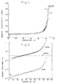
- FIG. 1 depicts the magnetic a.c. susceptibility as a function of temperature of a passivated Y1Ba2Cu3O x (3,500 ⁇ ) thin film prior to passivation (Curve 10 ; ⁇ ) and subsequent to passivation, employing a film of MgO (1,000 ⁇ ) after heating to 500°C (Curve 12 ; ⁇ ). It can be seen that the T c is substantially unchanged, and that the properties of the superconductor are nearly recovered as a result of the processing of the invention. The addition of a polyimide film (1 ⁇ m) and subsequent curing at 200°C had no effect on Curve 12.
- FIG. 2 depicts the microwave 100 GHz cavity surface resistance (R s ) measurements as a function of temperature on a film such as described in connection with FIG. 1, prior to passivation ( ⁇ ) and subsequent to passivation ( ⁇ ), employing the MgO film of FIG. 1.
- the R s performance of the YBCO film before and after passivation was the same.
- FIG. 2 also depicts the calculated curve at 10 GHz, which is based on f2 projection. Although this is a calculated result, it is to be compared with the single data point at 14, which is a stripline measurement at 4.2K and 10 GHz. The extrapolation of data is seen to be consistent with the measurement.
- FIG. 2 shows that the YBCO films are deposited reproducibly and that the results obtained for R s using different techniques are in agreement; and that the sputtered amorphous MgO film does not degrade the superconducting performance of a YBCO thin film.
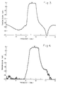
- YBCO microstrip X-band bandpass filters were constructed, with and without MgO passivation. The results are depicted in FIGS. 3 and 4, respectively.
- the passivated device also had a film of polyimide deposited over the top of the MgO thin film after the heating cycle.
- Both 6-pole filters were fabricated using YBCO films originating from the same 2 inch coated LaAlO3 substrate, so that the film composition and other parameters were similar. As can be seen from the insertion loss for devices with and without MgO, there is essentially no measurable difference between them; the uncertainty in the measured insertion loss is ⁇ 0.15 dB.
- the Table below lists the onset of superconductivity and the breadth of the transition temperature resulting from depositing on the superconductor (a) an amorphous MgO layer, (b) an amorphous MgO layer plus polyimide (the passivating layer of the invention), (c) a crystalline MgO layer, (d) a BF2 layer, (e) a BF2 layer plus polyimide, (f) a BaTiO3 layer, (g) a BaTiO3 layer plus polyimide, and (h) a polyimide layer.
- the process of the invention employing amorphous MgO, sintering, and polyimide overlayer, provides a coated superconductor that has substantially the same T c after processing as before. With other coatings, the T c is either lost or so broadened as to be useless as a superconductor.
Landscapes
- Engineering & Computer Science (AREA)
- Manufacturing & Machinery (AREA)
- Inorganic Compounds Of Heavy Metals (AREA)
- Superconductor Devices And Manufacturing Methods Thereof (AREA)
- Superconductors And Manufacturing Methods Therefor (AREA)
- Crystals, And After-Treatments Of Crystals (AREA)
Applications Claiming Priority (2)
| Application Number | Priority Date | Filing Date | Title |
|---|---|---|---|
| US608120 | 1990-11-01 | ||
| US07/608,120 US5114910A (en) | 1990-11-01 | 1990-11-01 | Passivation of thin film oxide superconductors |
Publications (2)
| Publication Number | Publication Date |
|---|---|
| EP0484010A2 true EP0484010A2 (de) | 1992-05-06 |
| EP0484010A3 EP0484010A3 (en) | 1993-09-22 |
Family
ID=24435125
Family Applications (1)
| Application Number | Title | Priority Date | Filing Date |
|---|---|---|---|
| EP19910309585 Withdrawn EP0484010A3 (en) | 1990-11-01 | 1991-10-17 | Passivation of thin film oxide super-conductors |
Country Status (3)
| Country | Link |
|---|---|
| US (1) | US5114910A (de) |
| EP (1) | EP0484010A3 (de) |
| JP (1) | JPH04300208A (de) |
Cited By (1)
| Publication number | Priority date | Publication date | Assignee | Title |
|---|---|---|---|---|
| DE4304573A1 (de) * | 1993-02-16 | 1994-08-18 | Forschungsgesellschaft Fuer In | Passivierungsschicht für Hochtemperatur-Supraleiter und Verfahren zu ihrer Aufbringung |
Families Citing this family (3)
| Publication number | Priority date | Publication date | Assignee | Title |
|---|---|---|---|---|
| US5425932A (en) * | 1993-05-19 | 1995-06-20 | Bell Communications Research, Inc. | Method for synthesis of high capacity Lix Mn2 O4 secondary battery electrode compounds |
| US6517944B1 (en) | 2000-08-03 | 2003-02-11 | Teracomm Research Inc. | Multi-layer passivation barrier for a superconducting element |
| JP4946309B2 (ja) * | 2006-09-25 | 2012-06-06 | 住友電気工業株式会社 | Bi系超電導体、超電導線材および超電導機器 |
Family Cites Families (2)
| Publication number | Priority date | Publication date | Assignee | Title |
|---|---|---|---|---|
| JPS63318015A (ja) * | 1987-06-19 | 1988-12-26 | Hitachi Ltd | 酸化物超電導体とその製法 |
| DE3889160T2 (de) * | 1987-07-27 | 1994-11-03 | Sumitomo Electric Industries | Supraleitender Dünnfilm und Verfahren, um diesen zu präparieren. |
-
1990
- 1990-11-01 US US07/608,120 patent/US5114910A/en not_active Expired - Lifetime
-
1991
- 1991-10-17 EP EP19910309585 patent/EP0484010A3/en not_active Withdrawn
- 1991-11-01 JP JP3287762A patent/JPH04300208A/ja active Pending
Cited By (1)
| Publication number | Priority date | Publication date | Assignee | Title |
|---|---|---|---|---|
| DE4304573A1 (de) * | 1993-02-16 | 1994-08-18 | Forschungsgesellschaft Fuer In | Passivierungsschicht für Hochtemperatur-Supraleiter und Verfahren zu ihrer Aufbringung |
Also Published As
| Publication number | Publication date |
|---|---|
| JPH04300208A (ja) | 1992-10-23 |
| US5114910A (en) | 1992-05-19 |
| EP0484010A3 (en) | 1993-09-22 |
Similar Documents
| Publication | Publication Date | Title |
|---|---|---|
| CN1022654C (zh) | 隧道型约瑟夫森器件及其制造方法 | |
| EP0299870B1 (de) | Verfahren zum Herstellen einer supraleitenden Dünnschicht | |
| EP0662724B1 (de) | Filme aus oxydischen Supraleitern mit hohem Tc | |
| US4957899A (en) | Method of patterning superconducting oxide thin films | |
| US5272133A (en) | Passivation of thin film oxide superconductors | |
| US5114910A (en) | Passivation of thin film oxide superconductors | |
| EP0341148A2 (de) | Halbleitersubstrat mit dünner Supraleiterschicht | |
| CA1309904C (en) | Method of producing a superconductive oxide layer on a substrate | |
| AU2185992A (en) | Process for making superconducting tl-pb-sr-ca-cu oxide films and devices | |
| EP0494830B1 (de) | Verfahren zur Herstellung eines Tunnelüberganges von der Art einer Josephson-Einrichtung aufgebaut aus supraleitendem oxydischem Verbundmaterial | |
| JP2501035B2 (ja) | 超電導薄膜 | |
| JP3058515B2 (ja) | 超電導ジョセフソン素子およびその製法 | |
| US5104850A (en) | Preparation of high temperature superconducting coated wires by dipping and post annealing | |
| EP0624910A1 (de) | Supraleiter und Herstellungsverfahren | |
| EP0517560B1 (de) | Verfahren zum Herstellen eines Substrats für supraleitende Mikrowellen-Komponenten | |
| JPH01111718A (ja) | 超電導薄膜の形成方法 | |
| KR0174382B1 (ko) | 고온 초전도 박막의 제조방법 | |
| Ivanov et al. | Superconducting Bi-Sr-Ca-Cu-O Thin Films Prepared by rf Magnetron Sputtering | |
| Chow et al. | Processing and characterization of high temperature superconductor films formed by spin-on coating and rapid thermal annealing | |
| US6156707A (en) | Method of manufacturing superconducting microwave component substrate | |
| JPS63303810A (ja) | セラミックス超電導体 | |
| JPH01140683A (ja) | 超電導薄膜の形成方法 | |
| JP2920496B2 (ja) | 酸化物分散粒子の形成方法 | |
| CN1045887A (zh) | 超导体制造方法 | |
| CA2057080A1 (en) | Process of forming a high temperature superconductor on a metal substrate surface |
Legal Events
| Date | Code | Title | Description |
|---|---|---|---|
| PUAI | Public reference made under article 153(3) epc to a published international application that has entered the european phase |
Free format text: ORIGINAL CODE: 0009012 |
|
| AK | Designated contracting states |
Kind code of ref document: A2 Designated state(s): DE FR GB IT NL |
|
| PUAL | Search report despatched |
Free format text: ORIGINAL CODE: 0009013 |
|
| AK | Designated contracting states |
Kind code of ref document: A3 Designated state(s): DE FR GB IT NL |
|
| 17P | Request for examination filed |
Effective date: 19940228 |
|
| STAA | Information on the status of an ep patent application or granted ep patent |
Free format text: STATUS: THE APPLICATION HAS BEEN WITHDRAWN |
|
| 18W | Application withdrawn |
Withdrawal date: 19941104 |
|
| R18W | Application withdrawn (corrected) |
Effective date: 19941020 |