EP0341148A2 - Halbleitersubstrat mit dünner Supraleiterschicht - Google Patents
Halbleitersubstrat mit dünner Supraleiterschicht Download PDFInfo
- Publication number
- EP0341148A2 EP0341148A2 EP89401238A EP89401238A EP0341148A2 EP 0341148 A2 EP0341148 A2 EP 0341148A2 EP 89401238 A EP89401238 A EP 89401238A EP 89401238 A EP89401238 A EP 89401238A EP 0341148 A2 EP0341148 A2 EP 0341148A2
- Authority
- EP
- European Patent Office
- Prior art keywords
- thin film
- layer
- semiconductor substrate
- set forth
- superconducting
- Prior art date
- Legal status (The legal status is an assumption and is not a legal conclusion. Google has not performed a legal analysis and makes no representation as to the accuracy of the status listed.)
- Granted
Links
- 239000010409 thin film Substances 0.000 title claims abstract description 128
- 239000000758 substrate Substances 0.000 title claims abstract description 110
- 239000004065 semiconductor Substances 0.000 title claims abstract description 78
- 150000001875 compounds Chemical class 0.000 claims abstract description 61
- 239000013078 crystal Substances 0.000 claims abstract description 48
- MCMNRKCIXSYSNV-UHFFFAOYSA-N Zirconium dioxide Chemical compound O=[Zr]=O MCMNRKCIXSYSNV-UHFFFAOYSA-N 0.000 claims abstract description 30
- 229910052710 silicon Inorganic materials 0.000 claims abstract description 25
- 239000000463 material Substances 0.000 claims abstract description 20
- 229910052747 lanthanoid Inorganic materials 0.000 claims abstract description 14
- 150000002602 lanthanoids Chemical class 0.000 claims abstract description 14
- 229910052751 metal Inorganic materials 0.000 claims abstract description 11
- 239000002184 metal Substances 0.000 claims abstract description 11
- 238000000034 method Methods 0.000 claims description 38
- CPLXHLVBOLITMK-UHFFFAOYSA-N Magnesium oxide Chemical compound [Mg]=O CPLXHLVBOLITMK-UHFFFAOYSA-N 0.000 claims description 27
- 229910052727 yttrium Inorganic materials 0.000 claims description 14
- 238000005240 physical vapour deposition Methods 0.000 claims description 11
- 238000000151 deposition Methods 0.000 claims description 10
- 229910052689 Holmium Inorganic materials 0.000 claims description 5
- 229910052691 Erbium Inorganic materials 0.000 claims description 4
- 229910052688 Gadolinium Inorganic materials 0.000 claims description 4
- 229910052765 Lutetium Inorganic materials 0.000 claims description 4
- 229910052775 Thulium Inorganic materials 0.000 claims description 4
- 229910052769 Ytterbium Inorganic materials 0.000 claims description 4
- 229910052746 lanthanum Inorganic materials 0.000 claims description 4
- 229910004613 CdTe Inorganic materials 0.000 claims description 3
- 229910052692 Dysprosium Inorganic materials 0.000 claims description 3
- 229910052693 Europium Inorganic materials 0.000 claims description 3
- 229910000530 Gallium indium arsenide Inorganic materials 0.000 claims description 3
- GPXJNWSHGFTCBW-UHFFFAOYSA-N Indium phosphide Chemical compound [In]#P GPXJNWSHGFTCBW-UHFFFAOYSA-N 0.000 claims description 3
- 229910000661 Mercury cadmium telluride Inorganic materials 0.000 claims description 3
- 229910052779 Neodymium Inorganic materials 0.000 claims description 3
- 229910052772 Samarium Inorganic materials 0.000 claims description 3
- 229910052797 bismuth Inorganic materials 0.000 claims description 3
- 229910052737 gold Inorganic materials 0.000 claims description 3
- WPYVAWXEWQSOGY-UHFFFAOYSA-N indium antimonide Chemical compound [Sb]#[In] WPYVAWXEWQSOGY-UHFFFAOYSA-N 0.000 claims description 3
- SBIBMFFZSBJNJF-UHFFFAOYSA-N selenium;zinc Chemical compound [Se]=[Zn] SBIBMFFZSBJNJF-UHFFFAOYSA-N 0.000 claims description 3
- 229910052709 silver Inorganic materials 0.000 claims description 3
- 229910002076 stabilized zirconia Inorganic materials 0.000 claims description 3
- 229910052716 thallium Inorganic materials 0.000 claims description 3
- VWQVUPCCIRVNHF-UHFFFAOYSA-N yttrium atom Chemical compound [Y] VWQVUPCCIRVNHF-UHFFFAOYSA-N 0.000 claims description 3
- 229910001218 Gallium arsenide Inorganic materials 0.000 claims 2
- XUIMIQQOPSSXEZ-UHFFFAOYSA-N Silicon Chemical compound [Si] XUIMIQQOPSSXEZ-UHFFFAOYSA-N 0.000 abstract description 24
- 239000010703 silicon Substances 0.000 abstract description 23
- 239000002887 superconductor Substances 0.000 description 30
- 238000004544 sputter deposition Methods 0.000 description 26
- 239000000523 sample Substances 0.000 description 20
- 238000002441 X-ray diffraction Methods 0.000 description 17
- 239000000843 powder Substances 0.000 description 16
- 239000010949 copper Substances 0.000 description 13
- 239000007789 gas Substances 0.000 description 12
- 239000000203 mixture Substances 0.000 description 10
- 230000000052 comparative effect Effects 0.000 description 7
- QVGXLLKOCUKJST-UHFFFAOYSA-N atomic oxygen Chemical compound [O] QVGXLLKOCUKJST-UHFFFAOYSA-N 0.000 description 6
- 238000005229 chemical vapour deposition Methods 0.000 description 6
- 239000001301 oxygen Substances 0.000 description 6
- 229910052760 oxygen Inorganic materials 0.000 description 6
- 238000000634 powder X-ray diffraction Methods 0.000 description 6
- 206010021143 Hypoxia Diseases 0.000 description 5
- 229910008198 Zr2O Inorganic materials 0.000 description 5
- 229910052788 barium Inorganic materials 0.000 description 5
- 230000008021 deposition Effects 0.000 description 5
- 239000002784 hot electron Substances 0.000 description 5
- JBRZTFJDHDCESZ-UHFFFAOYSA-N AsGa Chemical compound [As]#[Ga] JBRZTFJDHDCESZ-UHFFFAOYSA-N 0.000 description 4
- 229910009203 Y-Ba-Cu-O Inorganic materials 0.000 description 4
- 229910052802 copper Inorganic materials 0.000 description 4
- 239000010408 film Substances 0.000 description 4
- 238000001755 magnetron sputter deposition Methods 0.000 description 4
- 239000011159 matrix material Substances 0.000 description 4
- 230000000737 periodic effect Effects 0.000 description 4
- 238000005245 sintering Methods 0.000 description 4
- 229910015901 Bi-Sr-Ca-Cu-O Inorganic materials 0.000 description 3
- 229910002480 Cu-O Inorganic materials 0.000 description 3
- 229910002370 SrTiO3 Inorganic materials 0.000 description 3
- 230000002950 deficient Effects 0.000 description 3
- 238000009792 diffusion process Methods 0.000 description 3
- 238000005516 engineering process Methods 0.000 description 3
- 238000001451 molecular beam epitaxy Methods 0.000 description 3
- 239000002245 particle Substances 0.000 description 3
- 238000001552 radio frequency sputter deposition Methods 0.000 description 3
- 229910052712 strontium Inorganic materials 0.000 description 3
- VTYYLEPIZMXCLO-UHFFFAOYSA-L Calcium carbonate Chemical compound [Ca+2].[O-]C([O-])=O VTYYLEPIZMXCLO-UHFFFAOYSA-L 0.000 description 2
- MYMOFIZGZYHOMD-UHFFFAOYSA-N Dioxygen Chemical compound O=O MYMOFIZGZYHOMD-UHFFFAOYSA-N 0.000 description 2
- 229910000750 Niobium-germanium Inorganic materials 0.000 description 2
- 238000000137 annealing Methods 0.000 description 2
- WMWLMWRWZQELOS-UHFFFAOYSA-N bismuth(iii) oxide Chemical compound O=[Bi]O[Bi]=O WMWLMWRWZQELOS-UHFFFAOYSA-N 0.000 description 2
- 230000015271 coagulation Effects 0.000 description 2
- 238000005345 coagulation Methods 0.000 description 2
- 239000004020 conductor Substances 0.000 description 2
- 238000001816 cooling Methods 0.000 description 2
- RKTYLMNFRDHKIL-UHFFFAOYSA-N copper;5,10,15,20-tetraphenylporphyrin-22,24-diide Chemical compound [Cu+2].C1=CC(C(=C2C=CC([N-]2)=C(C=2C=CC=CC=2)C=2C=CC(N=2)=C(C=2C=CC=CC=2)C2=CC=C3[N-]2)C=2C=CC=CC=2)=NC1=C3C1=CC=CC=C1 RKTYLMNFRDHKIL-UHFFFAOYSA-N 0.000 description 2
- 229910001882 dioxygen Inorganic materials 0.000 description 2
- 230000000694 effects Effects 0.000 description 2
- 239000008187 granular material Substances 0.000 description 2
- 239000012212 insulator Substances 0.000 description 2
- 229910052749 magnesium Inorganic materials 0.000 description 2
- 229910052706 scandium Inorganic materials 0.000 description 2
- 229910021521 yttrium barium copper oxide Inorganic materials 0.000 description 2
- 229910052684 Cerium Inorganic materials 0.000 description 1
- RYGMFSIKBFXOCR-UHFFFAOYSA-N Copper Chemical compound [Cu] RYGMFSIKBFXOCR-UHFFFAOYSA-N 0.000 description 1
- 230000005668 Josephson effect Effects 0.000 description 1
- 229910003098 YBa2Cu3O7−x Inorganic materials 0.000 description 1
- 229910045601 alloy Inorganic materials 0.000 description 1
- 239000000956 alloy Substances 0.000 description 1
- 229910052790 beryllium Inorganic materials 0.000 description 1
- 238000009835 boiling Methods 0.000 description 1
- 229910052791 calcium Inorganic materials 0.000 description 1
- 229910000019 calcium carbonate Inorganic materials 0.000 description 1
- 235000010216 calcium carbonate Nutrition 0.000 description 1
- 239000000919 ceramic Substances 0.000 description 1
- 229910010293 ceramic material Inorganic materials 0.000 description 1
- 238000009770 conventional sintering Methods 0.000 description 1
- 230000006866 deterioration Effects 0.000 description 1
- 229910003460 diamond Inorganic materials 0.000 description 1
- 239000010432 diamond Substances 0.000 description 1
- 238000002003 electron diffraction Methods 0.000 description 1
- 238000005265 energy consumption Methods 0.000 description 1
- 238000005530 etching Methods 0.000 description 1
- 238000002474 experimental method Methods 0.000 description 1
- 239000010419 fine particle Substances 0.000 description 1
- 238000010438 heat treatment Methods 0.000 description 1
- 239000001307 helium Substances 0.000 description 1
- 229910052734 helium Inorganic materials 0.000 description 1
- SWQJXJOGLNCZEY-UHFFFAOYSA-N helium atom Chemical compound [He] SWQJXJOGLNCZEY-UHFFFAOYSA-N 0.000 description 1
- 239000012535 impurity Substances 0.000 description 1
- 230000010354 integration Effects 0.000 description 1
- 238000005468 ion implantation Methods 0.000 description 1
- 238000007733 ion plating Methods 0.000 description 1
- 238000004519 manufacturing process Methods 0.000 description 1
- 238000002488 metal-organic chemical vapour deposition Methods 0.000 description 1
- 238000001465 metallisation Methods 0.000 description 1
- 238000000059 patterning Methods 0.000 description 1
- 230000000704 physical effect Effects 0.000 description 1
- 238000005268 plasma chemical vapour deposition Methods 0.000 description 1
- 239000007787 solid Substances 0.000 description 1
- LEDMRZGFZIAGGB-UHFFFAOYSA-L strontium carbonate Chemical compound [Sr+2].[O-]C([O-])=O LEDMRZGFZIAGGB-UHFFFAOYSA-L 0.000 description 1
- 229910000018 strontium carbonate Inorganic materials 0.000 description 1
- 238000002230 thermal chemical vapour deposition Methods 0.000 description 1
- 230000007704 transition Effects 0.000 description 1
- 229910052720 vanadium Inorganic materials 0.000 description 1
Images


Classifications
-
- H—ELECTRICITY
- H10—SEMICONDUCTOR DEVICES; ELECTRIC SOLID-STATE DEVICES NOT OTHERWISE PROVIDED FOR
- H10N—ELECTRIC SOLID-STATE DEVICES NOT OTHERWISE PROVIDED FOR
- H10N60/00—Superconducting devices
- H10N60/01—Manufacture or treatment
- H10N60/0268—Manufacture or treatment of devices comprising copper oxide
- H10N60/0296—Processes for depositing or forming copper oxide superconductor layers
- H10N60/0576—Processes for depositing or forming copper oxide superconductor layers characterised by the substrate
- H10N60/0632—Intermediate layers, e.g. for growth control
-
- H—ELECTRICITY
- H10—SEMICONDUCTOR DEVICES; ELECTRIC SOLID-STATE DEVICES NOT OTHERWISE PROVIDED FOR
- H10N—ELECTRIC SOLID-STATE DEVICES NOT OTHERWISE PROVIDED FOR
- H10N60/00—Superconducting devices
- H10N60/01—Manufacture or treatment
- H10N60/0268—Manufacture or treatment of devices comprising copper oxide
- H10N60/0296—Processes for depositing or forming copper oxide superconductor layers
- H10N60/0576—Processes for depositing or forming copper oxide superconductor layers characterised by the substrate
- H10N60/0604—Monocrystalline substrates, e.g. epitaxial growth
-
- H—ELECTRICITY
- H10—SEMICONDUCTOR DEVICES; ELECTRIC SOLID-STATE DEVICES NOT OTHERWISE PROVIDED FOR
- H10N—ELECTRIC SOLID-STATE DEVICES NOT OTHERWISE PROVIDED FOR
- H10N60/00—Superconducting devices
- H10N60/80—Constructional details
- H10N60/85—Superconducting active materials
- H10N60/855—Ceramic superconductors
Definitions
- the present invention relates to a semiconductor substrate having a superconducting thin film thereon and a process for producing the same.
- a single crystal semiconductor substrate having a superconducting thin film which is uniform in composition and possesses a high critical temperature (Tc) and a high critical current density (Jc) and a process for producing the same.
- the superconducting thin film layer deposited on the semiconductor substrate according to the present invention can be used as a wiring material for integrated circuits which are built in the semiconductor substrate and for Josephson junctions in Josephson devices.
- the semiconductor substrate according to the present invention can be used as a material for fabricating a novel circuit element which utilizes "an aproximity effect" between a semiconductor and a superconductor such as a superconducting transistor or a hot-electron transistor.
- the superconductivity is a phenomenon which is explained to be a kind of phase changes of electrons under which the electric resistance become zero and the perfect diamagnetism is observed.
- Several superconducting devices have been proposed and developed in electronics which is a typical field to which the superconducting phenomenon is applicable.
- a typical application of the superconductor is Josephson device in which quantum efficiency is observed macroscopically when an electric current is passed through a weak junction arranged between two superconductors.
- the tunnel junction type Josephson device is expected to be a high-speed and low-power consuming switching device owing to smaller energy gap of the superconducting material. It is also expected to utilize the Josephson device as a high-sensitive sensor or detector for sensing very weak magnetic field, microwave, radiant ray or the like since variation of electromagnetic wave or magnetic field is reflected in variation of Josephson effect and can be observed as a precise quantum phenomenon.
- one of the basic technologies for fabricating an integrated circuit on a silicon single crystal substrate is a metallization technology for forming patterned conductor lines which are used for interconnecting a variety of electronic elements which are fabricated by the other basic technology including an insulating layer forming stage, a patterning stage of the insulating layer and an impurity doping stage by means of thermal diffusion, ion implantation or the like.
- Tc critical temperature
- the new type compound oxide superconductor discovered by Bednorz and Müller is represented by [La,Sr]2CuO4 which is called the K2NiF4-type oxide having a crystal stucture which is similar to known perovskite type oxides.
- the K2NiF4-type compound oxides show such higher Tc as 30 K which are extremely higher than known superconducting materials.
- the other type new superconducting materials which were reported recently are a compound oxide of Bi-Sr-Ca-Cu-O system reported by Maeda et al (Japanese journal of Applied Physics. Vol. 27, No. 2, p 1209 to 1210) and Tl-Ba-Ca-Cu-O system which exhibit such high Tc as more than 100 K (Hermann et al. Appl. Phys. Lett. 52 (20) p1738) and which are chemically much stable than the abovementioned YBCO type compound oxide or the like. And hence, the possibility of an actual utilization of the high Tc superconductors have burst onto the scene.
- the above-mentioned new type superconducting materials can be deposited on a substrate in a form of a thin film by physical vapour deposition (PVD) technique or chemical vapor deposition (CVD) technique.
- PVD physical vapour deposition
- CVD chemical vapor deposition
- a vapour source or a target of an oxide which is prepared by sintering technique is vaporized or sputtered to deposit a thin film of superconductor which is then subjected to an after-treatment in which the thin film deposited is heated or annealed in an oxygen-containing atmospher or which is exposed to oxygen plasma.
- Such after-treatment is indispensable for realize desired superconducting properties because the superconducting properties of the above-mentioned new type compound oxide superconductors are influenced by the oxygen deficiency in the crystal. In fact, if the oxygen deficiency in the crystal is not proper, Tc can not become higher and a discrepancy between the onset temperature and a temperature where perfect zero resistance is observed become big.
- the conventional sputtering technique for preparing a thin film composed of the ceramics type oxide superconductors represented by the formula BaPb 1-x Bi x O3 (in which 0.05 ⁇ x ⁇ 0.35) is disclosed in Japanese patent laid-open No. 56-10,9824.
- the superconducting thin film which is represented in an oxygen-containing atmosphere by high-frequency sputtering technique while the substrate is heated in order to improve ordering or orientation of the crystal.
- the resulting film deposited on the substrate is further heat-treated at 500 to 550°C in order to increase the oxygen-content in the thin film but mentions nothing about the conditions how to prepare the thin film of high-Tc superconductor which was discovered after the filing date of this patent.
- the substrates on which the thin films of the new type superconductors are deposited are limited to very special materials such as single crystal oxides of MgO, SrTiO3 or the like because the substrates are required to have the same or similar lattice constants as the superconducting thin film to be deposited in order to realize desired crystalline structures of superconductors.
- the single crystal oxides such as MGO OR SrTiO3 possess similar lattice constants to the new type superconductor and are chemically stable, they have been usually used as the substrate. However, they are not semiconductors but insulators.
- the substrate on which the superconducting thin film is deposited must be heated at a high temperature of about 700 C° during the sputtering operation. Therefore, when a semiconductor substrate such as a silicon substrate is used, an element of the substrate such as silicon diffuses into the superconducting thin film layer, resulting in deterioration of superconducting property.
- the desired crystalline structure of superconductor can not be realized in the thin film because of mismatch of lattice constants between the superconductor and the semiconductor.
- fine cracks are produced in the superconducting thin film deposited because of difference in thermal expansion coefficient between the superconductor and the semiconductor.
- An object of the present invention is to provide a semiconductor substrate having a superconducting thin film thereon and a process for producing the same.
- the present invention provides a semiconductor substrate having a thin film of a superconducting material composed of a compound oxide whose critical temperature is higher higher than 30 K, characterized in that the superconducting thin film is formed on a buffer layer which is deposited on a surface of the semiconductor substrate.
- the semiconductor substrates to which the present invention is applicable are preferably silicon (Si) single crystal and gallium arsenic (GaAs) single crystal which are actually used as substrates for integrated circuits.
- the present invention is also applicable to the other compound semiconductor substrates such as GaP, InP, ZnSe, InSb, 3C-SiC, 6H-SiC, InAlAs, GaInAs, InGaAsP, HgCdTe, GaAlAs and CdTe which are under developing stage.
- the substrate can be a diamond substrate.
- the buffer layer is deposited on ⁇ 100 ⁇ plane of a silicon single crystal substrate.
- the essence of the present invention reside in that a buffer layer is interposed between the semiconductor substrate and the superconductor thin film layer.
- the buffer layer has preferably a thickness of more than 50 ⁇ , more preferably in a range of 50 to 1,000 ⁇ . Diffusion of silicon element into the superconducting thin film layer can be prevented effectively by the buffer layer of more than 50 ⁇ so that an improved superconducting thin film layer is produced.
- the buffer layer is made of ZrO2 or MgO which has one of the following structures:
- the superconducting thin film layer deposited shows a c-axis oriented crystalline structure or becomes a single crystal.
- the term c-axis oriented crystalline structure includes any crystal whose c-axis is inclined at a certain angle with respect to a surface of the thin film in addition to a crystal whose c-axis is perpendicular thereto.
- the buffer layer interposed between the superconducting thin film and the semiconductor substrate according to the present invention prevents mutual diffusion between elements of the superconductor and the semiconductor, so that a thin film of superconductor of compound oxide having high Tc can be deposited on the semiconductor.
- the buffer layer is made of a compound layer composed of at least one metal and at least one oxide.
- the buffer layer made of the compound layer permits to produce a thin film layer of superconducting compound oxide of high quality which has no micro cracks.
- the metal element of the compound oxide has preferably a fine crystalline structure which embedded in a crystalline structure of the oxide.
- metal element exists at a constant relation with respect to the crystalline structure of the oxide.
- the oxide and the metal of which the compound layer is composed have similar lattice constants to each other and are little diffuse into the superconducting compound oxide thin film layer.
- the compound layer is preferably composed of an oxide selected from ZrO2, MgO or yttrium stabilized zirconia (YSZ) and a metal selected from Ag or Au.
- the buffer layer composed of the compound layer is interposed between the semiconductor substrate and the superconducting thin film layer, the condition of an interface between them are much improved than the first embodiment in which the buffer layer is made of oxide only so that the the properties of the semiconductor are also improved.
- much higher critical current density (Jc) can be passed through the superconducting thin film layer deposited because the thin film shows a c-axis oriented crystalline structure or becomes a single crystal and also because the thin film has no micro cracks.
- the compound layer as a buffer layer may be produced by a physical vapour deposition technique such as molecular beam epitaxy (MBE).
- the superconducting thin film having a composition of Y1Ba2Cu3O7 formed on the buffer layer deposited on the semiconductor according to the present invention has a X-ray diffraction pattern which is characterized by the following points:
- the superconducting compound oxide of Ba, Y and Cu has preferably a X-ray diffraction pattern shown in Figure 1.
- the superconducting thin film layer which can be deposited on the semiconductor substrate through the buffer layer according to the present invention can be made of any one of compound oxide type superconducting materials having the critical temperature of higher than 30 K including the following known compound oxides:
- the element ⁇ of IIa group element is preferably Ba, Sr, Ca, Mg, Be or the like. More preferably the element ⁇ is Ba and Sr from 10 % to 80 % of which may be replaced by one or two elements selected from a group comprising Mg an Ca.
- the element ⁇ of IIIa group element is preferably Sc, Y, La and lanthanide elements such as Ce, Gd, Ho, Er, Tm, Yb or Lu. More preferably the element ⁇ is Y, La or Ho from 10 % to 80 % of which may be replaced by Sc or one or two elements selected from the other lanthanide elements.
- the ⁇ is usually copper a part of which can be replaced by the other element selected from a group comprising Ib, IIb, IIIb, IVa and VIIIa groups of the Periodic Table such as Ti or V.
- These systems are thought to have quasi-perovskite type crystal structure such as oxygen deficient orthorombic crystal structure or the like. More particularly, they can be the following compound oxides:
- (1-1) a compound oxides represented by the general formula: (La 1-x Sr x )2CuO 4-a in which, 0 ⁇ x ⁇ 1 and 0 ⁇ a ⁇ 1.
- Ln stands for an element selected from Y, La or lanthanide elements
- Cu a compound oxide of Ba, Ln (Ln stands for an element selected from Y, La or lanthanide elements) and Cu and represented by the general formula: Ln1Ba2Cu3O 7- ⁇ in which Ln stands for Y or at least one lanthanide element selected from a group comprising La, Nd, Sm, Eu, Gd, Dy, Ho, Er, Yb, Tm and Lu and ⁇ is a number which satisfies a range of 0 ⁇ ⁇ ⁇ 1.
- this type compound oxides include following systems: Y1Ba2Cu3O 7- ⁇ , Ho1Ba2Cu3O 7- ⁇ , Lu1Ba2Cu3O 7- ⁇ , SM1Ba2Cu3O 7- ⁇ , Nd1Ba2Cu3O 7- ⁇ , Gd1Ba2Cu3O 7- ⁇ , Eu1Ba2Cu3O 7- ⁇ , Er1Ba2Cu3O 7- ⁇ , Dy1Ba2Cu3O 7- ⁇ , Tm1Ba2Cu3O 7- ⁇ , Yb1Ba2Cu3O 7- ⁇ , La1Ba2Cu3O 7- ⁇ , in which ⁇ is a number which satisfies a range of 0 ⁇ ⁇ ⁇ 1 and possess preferably perovskite type or quasi-perovskite type crystal structure.
- quasi-perovskite type means a structure which can be considered to have such a crystal structure that is similar to perovskite-type oxides and includes an orthorhombically distorted perovskite or a distorted oxygen-deficient perovskite or the like.
- An atomic ratio of the lanthanide element "Ln":Ba:Cu is preferably 1 : 2: 3 as is defined by the formula but the atomic ratio is not restricted strictly to this ratio. In fact, the other compound oxides having different atomic ratios which are deviate from the above-mentioned values by 10 % may exhibit superconducting property.
- this type compound oxides include the following systems: Bi4Sr4Ca4Cu6O 20-r, Bi2Sr2Ca2Cu3O 10-r, Tl4Ba4Ca4Cu6O 20-r, Tl2Ba2Ca2Cu3O 10-r, in which r is a number which satisfies a range of -2 ⁇ r ⁇ +2.
- the present invention is applicable to the other compound oxides.
- the superconducting thin film layer can be removed locally by etching technique or the like so that the superconducting thin film layer is shaped into a desired circuit pattern.
- the superconducting thin film layer deposited on the semiconductor substrate according to the present invention can be used as a wiring material for semiconductor circuits which are built in the substrate or as an element of a superconducting transistor.
- the semiconductor substrate according to the present invention can be used also as a substrate for fabricating an integrated circuit for building novel superconducting elements or as a substrate on which electronic devices are built. For example, Josephson junctions can be fabricated in the superconducting thin film to built Josephson devices.
- the semiconductor substrate according to the present invention can be used also for fabricating high-speed semiconductor devices such as superconducting transistors having more than three electrodes, superconducting FETs or hot electron transistors which utilized the interface between the superconducting thin film layer and the semiconductor substrate.
- high-speed semiconductor devices such as superconducting transistors having more than three electrodes, superconducting FETs or hot electron transistors which utilized the interface between the superconducting thin film layer and the semiconductor substrate.
- the present invention provides also a process for producing the above-mentioned semiconductor substrate having the thin film layer of superconducting compound oxide.
- the process according to the present invention comprises two steps of depositing a buffer layer on a surface of a semiconductor substrate and then depositing a superconducting thin film composed of a compound oxide whose critical temperature is higher than 30 K.
- PVD physical vapor deposition technique
- MBE molecular beam epitaxy
- CVD chemical vapor deposition
- the first step for producing the buffer layer can be effected by any one of known PVD and CVD techniques which are selected according to the kinds of semiconductor substrate, while the second step for producing the superconducting layer is preferably effected by PVD, preferably sputtering, more particularly high-frequency magnetron sputtering technique.
- the superconducting thin film produced by the high-frequency magnetron sputtering technique possesses a superior crystalline structure and shows improved oxygen deficiency.
- the superconducting thin film must be produced in oxygen-containing atmosphere in order to control the oxygen deficiency in the thin film deposited because the superconducting properties are influenced by the oxygen deficiency in the thin film.
- the semiconductor substrate of single crystal is heated above 550 °C but below 750 °C, the power density supplied to a target is selected between 1 W/cm2 and 6 W/cm2 and a distance from the target to the semiconductor substrate is selected between 20 mm and 40 mm.
- the substrate temperature exceed 750 °C, the physical properties of the semiconductor single crystal are spoiled and also a reaction occur between the semiconductor material and the compound oxide of which the superconducting thin film is composed.
- the substrate temperature is not higher than 550 °C, the crystalline compound oxide of superconductor can not be obtained so that it is impossible or difficult to prepare a thin film having desired superconducting properties.
- the power density supplied to a target exceed 6 W/cm2 and when the distance from the target to the semiconductor substrate is not longer than 20 mm, uniformity of the thin film deposited is lost and hence the critical current density (Jc) become lower.
- the composition of the target used in the second step for producing the superconducting thin film can be determined by persons skilled in the art by experiments and can be selected according to sputtering rates of vaporized elements, dimensions of a sputtering chamber or the like.
- the composition of the target can be adjusted to Y1Ba x Cu y O z in which 2 ⁇ x ⁇ 2.4, 4.2 ⁇ y ⁇ 5.5 and 7 ⁇ x ⁇ 10.
- the sputtering gas is preferably a mixed gas of Ar and O2 containing O2 gas of 10 to 50 %.
- O2 oxygen
- O2 containing O2 gas of 10 to 50 %.
- the content of O2 is not higher than 10 %, satisfactory oxygen can not be supplied.
- the O2 exceed 50 %, the sputtering rate becomes too slow and is not practical.
- a post-annealing or heat-treatment after deposition was indispensable in order to obtain a superconducting thin film of high quality.
- it can omit or shorten the after-treatment in oxygen gas at a high temperature because the thin film as grown is a layer of a high quality.
- the post-annealing can be omitted by introducing O2 gas into a sputtering chamber just after deposition.
- the buffer layer of MgO is preferably deposited on a predetermined plane of the semiconductor substrate in order to obtain the superconducting thin film of high quality whose crystal structure is oriented to c-axis on the substrate "as grown". Selection of the crystal plane depend on the combination of the semiconductor and the buffer layer. In fact, the structure and the crystalline orientation of the buffer layer depend on the plane of the semiconductor as an under-layer. For example, in a case that a buffer layer of MgO is formed on a silicon single crystal semiconductor substrate, the buffer layer is preferably deposited on ⁇ 100 ⁇ plane of the silicon substrate in order to assure orientation of the crystalline structure of the superconducting thin film deposited.
- the superconducting thin films of the above-mentioned type compound oxides shows anisotropy in the critical current density. Namely, the current passing along a direction which is in parallel with a plane defined by a-axis and b-axis of the crystal show a very high critical current density, while the current passing along the other directions is relatively lower. Therefore, in this case, the c-axis of the superconducting thin film become nearly perpendicular to a surface of a substrate, so that the critical current density is improved greatly. If the buffer layer is not interposed between the semiconductor substrate and the superconducting thin film, silicon atoms diffuse into the superconducting thin film, so that the thin film obtained shows deteriorated superconducting properties and possesses lower critical current density.
- the condition of an interface between them is improved greatly comparing to the conventional ones owing to reduced discrepancy in thermal expansion coefficient so that the semiconductor devices which utilize the combination of the superconductor and the semiconductor can be realized.
- the films according to the present invention have higher Jc than conventional superconducting thin film and hence they can be utilized advantageously in a applications of thin film devices, such as Matisoo switching elements or Josephson device, Anacker memory device or Superconducting Quantum Interference Device (SQUID) as well as high-speed semiconductor devices combined with a superconductor and having more than three terminals such as a superconducting transistor or superconducting FET or the like.
- thin film devices such as Matisoo switching elements or Josephson device, Anacker memory device or Superconducting Quantum Interference Device (SQUID) as well as high-speed semiconductor devices combined with a superconductor and having more than three terminals such as a superconducting transistor or superconducting FET or the like.
- a buffer layer of Zr2O having a thickness of 500 ⁇ is deposited on a ⁇ 100 ⁇ plane of a single crystal of silicon substrate in a sputtering machine by using a target made of sintered mass of Zr2O under the following conditions: Pressure (total) : 2 x 10 ⁇ 2 Torr Sputtering gas : Ar + O2 ( O2: 16 % ) Substrate temperature : 700 °C
- a superconducting thin film of Y-Ba-Cu-O type is deposited in a high-frequency magnetron sputtering machine by using the powder target on the buffer layer of Zr2O under the following conditions: Pressure (total) : 2 x 10 ⁇ 2 Torr Sputtering gas : Ar + O2 ( O2: 16 % ) Substrate temperature : 720 °C
- a resulting thin film obtained of 1,000 ⁇ thick is heated in oxygen gas stream at 700 °C for 24 hours and then cooled slowly at a cooling rate of 3 °C/min.
- the resulting thin film is polycrystal whose c-axis is oriented to a surface of the substrate and have a composition of YBa2Cu 4.5 O 7-k (K is a number satisfies 0 ⁇ k ⁇ 1).
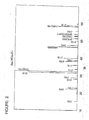
- the thin film is measured by a X-ray diffraction analyzer (Rigaku Denki Co., Ltd) with K ⁇ of Cu to obtain a X-ray diffraction pattern of the thin film shown in Fig. 1.
- Fig. 2 is a powder X-ray diffraction chart observed in a known powder sample represented by Y1Ba2Cu3O7 which is used as a reference.
- I100 an intensity of the most intense peak in the powder X-ray diffraction chart (Fig. 2) measured in the powder sample of Y1Ba2Cu3O7
- Iz an intensity of the (00n) plane in the powder X-ray diffraction chart, wherein n is an integer
- J100 an intensity of a crystal face which has the same index of the crystal face as the most intense peak in the powder X-ray diffraction chart (Fig. 2) and which is observed in a X-ray diffraction chart measured in the thin film of the present invention
- J w an intensity of the (00n) plane in the X-ray diffraction chart measured in the thin film of the present invention.
- Fig. 3 is a X-ray diffraction chart observed in the resulting thin film of Sample 1 and shows that the thin film is well-oriented to c-axis. Sample 2 and 3 also show similar X-ray diffraction chart.
- a buffer layer of MgO is deposited by sputtering on ⁇ 100 ⁇ plane of a silicon substrate under the conditions listed in Table 6.
- Table 6 Sample No substrate temperature crystalline condition thickness ( ⁇ ) 1 200 °C amorphous 500 2 500 °C cubic ⁇ 100 ⁇ oriented 80 3 700 °C cubic ⁇ 111 ⁇ single crystal 300 RF power : 200 W Pressure : 2 x 10 ⁇ 2 Torr Sputtering gas : Ar + O2 ( O2: 20 % )
- X-ray diffraction charts observed in the resulting thin films of Sample 1 to 3 are same as Fig. 3 in Example 2 and show that the thin film is well-oriented to C-axis.
- Tc critical temperatures
- a buffer layer of a compound film composed of MgO and Ag is deposited by MBE process in which MgO and Ag are evaporated simultaneously onto a silicon substrate under the following conditions: Substrate temperature : 500 °C Gas pressure : 1 x 10 ⁇ 6 Torr Atmosphere : O2 gas Thickness of thin film : 300 ⁇
- the thin film of superconducting compound oxide is determined to be a single crystal by electron diffraction analyzer.
- Three samples are prepared by depositing three superconducting thin film layers of Y-Ba-Cu-O system, Ho-Ba-Cu-O system and Bi-Sr-Ca-Cu-O system on the ZrO2 buffer layer respectively.
- Each of the superconducting thin films is deposited by magnetron RF sputtering technique which is itself known.
- Targets used in the sputtering are prepared by the conventional sintering technique to obtain sintered powder of YBa2Cu 4.5 O x for Y-Ba-Cu-O system and HoBa 2.2 Cu 4.7 O x for Ho-Ba-Cu-O system respectively.
- the resulting samples of semiconductor substrates having the superconducting thin film layer show good condition at an interface between the semiconductor substrate and the buffer layer and between the buffer layer and the superconducting thin film layer which are requested in semiconductor devices.
- the following table shows the resulting critical temperature Tc (a temperature where the phenomenon of superconductivity start to be observed), Tci (a temperature where zero resistance is observed) and the critical current density determined at 77 K of the superconducting thin films of respective samples.
- Example 9 The same operation as Example 9 is repeated except that the semiconductor substrate of silicon is replaced by a single crystal of gallium arsenic (GaAs).
- GaAs gallium arsenic
- substrate temperature during the sputtering operation is lowered down from 650 °C to 300 °C.
Landscapes
- Engineering & Computer Science (AREA)
- Manufacturing & Machinery (AREA)
- Chemical & Material Sciences (AREA)
- Ceramic Engineering (AREA)
- Crystallography & Structural Chemistry (AREA)
- Inorganic Compounds Of Heavy Metals (AREA)
- Superconductor Devices And Manufacturing Methods Thereof (AREA)
- Superconductors And Manufacturing Methods Therefor (AREA)
- Containers, Films, And Cooling For Superconductive Devices (AREA)
Applications Claiming Priority (38)
| Application Number | Priority Date | Filing Date | Title |
|---|---|---|---|
| JP108498/88 | 1988-04-30 | ||
| JP10849888 | 1988-04-30 | ||
| JP109323/88 | 1988-05-02 | ||
| JP10932488 | 1988-05-02 | ||
| JP109324/88 | 1988-05-02 | ||
| JP10932388 | 1988-05-02 | ||
| JP110011/88 | 1988-05-06 | ||
| JP110015/88 | 1988-05-06 | ||
| JP110017/88 | 1988-05-06 | ||
| JP63110013A JPH01280370A (ja) | 1988-05-06 | 1988-05-06 | 超電導体層を有する半導体基板 |
| JP11001188 | 1988-05-06 | ||
| JP110014/88 | 1988-05-06 | ||
| JP63110025A JPH01280382A (ja) | 1988-04-30 | 1988-05-06 | 超電導体層を有する半導体基板 |
| JP110016/88 | 1988-05-06 | ||
| JP63110015A JPH01280372A (ja) | 1988-05-06 | 1988-05-06 | 超電導体層を有する半導体基板 |
| JP63110020A JPH01280377A (ja) | 1988-05-06 | 1988-05-06 | 超電導体層を有する半導体基板 |
| JP110023/88 | 1988-05-06 | ||
| JP63110017A JPH01280374A (ja) | 1988-05-06 | 1988-05-06 | 超電導体層を有する半導体基板 |
| JP63110014A JPH01280371A (ja) | 1988-05-06 | 1988-05-06 | 超電導体層を有する半導体基板 |
| JP63110022A JPH01280379A (ja) | 1988-05-06 | 1988-05-06 | 超電導体層を有する半導体基板 |
| JP63110016A JPH01280373A (ja) | 1988-05-06 | 1988-05-06 | 超電導体層を有する半導体基板 |
| JP63110021A JPH01280378A (ja) | 1988-05-06 | 1988-05-06 | 超電導体層を有する半導体基板 |
| JP110021/88 | 1988-05-06 | ||
| JP63110023A JPH01280380A (ja) | 1988-05-06 | 1988-05-06 | 超電導体層を有する半導体基板 |
| JP110022/88 | 1988-05-06 | ||
| JP110018/88 | 1988-05-06 | ||
| JP110019/88 | 1988-05-06 | ||
| JP110013/88 | 1988-05-06 | ||
| JP110024/88 | 1988-05-06 | ||
| JP63110019A JPH01280376A (ja) | 1988-05-06 | 1988-05-06 | 超電導体層を有する半導体基板 |
| JP110012/88 | 1988-05-06 | ||
| JP110020/88 | 1988-05-06 | ||
| JP63110012A JPH01280369A (ja) | 1988-05-06 | 1988-05-06 | 超電導体層を有する半導体基板 |
| JP110025/88 | 1988-05-06 | ||
| JP63110018A JP2797186B2 (ja) | 1988-05-06 | 1988-05-06 | 超電導体層を有する半導体基板 |
| JP63110024A JPH01280381A (ja) | 1988-05-06 | 1988-05-06 | 超電導体層を有する半導体基板 |
| JP24942588 | 1988-10-03 | ||
| JP249425/88 | 1988-10-03 |
Publications (3)
| Publication Number | Publication Date |
|---|---|
| EP0341148A2 true EP0341148A2 (de) | 1989-11-08 |
| EP0341148A3 EP0341148A3 (en) | 1990-11-14 |
| EP0341148B1 EP0341148B1 (de) | 1994-10-12 |
Family
ID=27586278
Family Applications (1)
| Application Number | Title | Priority Date | Filing Date |
|---|---|---|---|
| EP89401238A Expired - Lifetime EP0341148B1 (de) | 1988-04-30 | 1989-05-02 | Halbleitersubstrat mit dünner Supraleiterschicht |
Country Status (5)
| Country | Link |
|---|---|
| EP (1) | EP0341148B1 (de) |
| KR (1) | KR900017216A (de) |
| AU (1) | AU614606B2 (de) |
| CA (1) | CA1330196C (de) |
| DE (1) | DE68918746T2 (de) |
Cited By (5)
| Publication number | Priority date | Publication date | Assignee | Title |
|---|---|---|---|---|
| US5314870A (en) * | 1990-06-28 | 1994-05-24 | Sumitomo Electric Industries, Ltd. | Preparing thin film of oxide superconductor |
| US5565415A (en) * | 1991-01-10 | 1996-10-15 | Sumitomo Electric Industries, Ltd. | Method for manufacturing tunnel junction type josephson device composed of compound oxide superconductor material |
| US5925892A (en) * | 1996-06-14 | 1999-07-20 | International Superconductivity Technology Center | Josephson junction element with an asymmetric groove providing a single weak link region |
| CN115428156A (zh) * | 2020-03-31 | 2022-12-02 | 微软技术许可有限责任公司 | 侧栅半导体-超导体混合器件 |
| CN120164669A (zh) * | 2025-02-25 | 2025-06-17 | 中国长江三峡集团有限公司 | 一种基底的涂层导体制备方法、装置、设备及存储介质 |
Families Citing this family (5)
| Publication number | Priority date | Publication date | Assignee | Title |
|---|---|---|---|---|
| AU610260B2 (en) * | 1987-10-16 | 1991-05-16 | Furukawa Electric Co. Ltd., The | Oxide superconductor shaped body and method of manufacturing the same |
| JPH0286014A (ja) * | 1988-06-17 | 1990-03-27 | Sumitomo Electric Ind Ltd | 複合酸化物超電導薄膜と、その成膜方法 |
| DE69016283T3 (de) * | 1989-06-30 | 1998-04-02 | Sumitomo Electric Industries | Substrat mit einer supraleitenden Schicht. |
| CA2043545C (en) * | 1990-05-30 | 1997-03-04 | Saburo Tanaka | Process for preparing superconducting junction of oxide superconductor |
| WO2021167315A1 (ko) * | 2020-02-18 | 2021-08-26 | 한양대학교 산학협력단 | 결정성 izto 산화물 반도체를 구비하는 박막트랜지스터 및 이의 제조방법 |
Family Cites Families (3)
| Publication number | Priority date | Publication date | Assignee | Title |
|---|---|---|---|---|
| AU615014B2 (en) * | 1987-02-17 | 1991-09-19 | Sumitomo Electric Industries, Ltd. | Superconducting thin film and wire and a process for producing the same |
| AU607219B2 (en) * | 1987-05-29 | 1991-02-28 | Toray Industries, Inc. | Method of forming superconductive thin films and solutions for forming the same |
| AU610260B2 (en) * | 1987-10-16 | 1991-05-16 | Furukawa Electric Co. Ltd., The | Oxide superconductor shaped body and method of manufacturing the same |
-
1989
- 1989-04-29 KR KR1019890005786A patent/KR900017216A/ko not_active Ceased
- 1989-05-01 CA CA000598305A patent/CA1330196C/en not_active Expired - Fee Related
- 1989-05-01 AU AU33896/89A patent/AU614606B2/en not_active Ceased
- 1989-05-02 DE DE68918746T patent/DE68918746T2/de not_active Expired - Fee Related
- 1989-05-02 EP EP89401238A patent/EP0341148B1/de not_active Expired - Lifetime
Non-Patent Citations (7)
| Title |
|---|
| APPLIED PHYSICS LETTERS. vol. 51, no. 13, 28 September 1987, NEW YORK US pages 1027 - 1029; M. GURVITCH et al: "Preparation and substrate reactions of superconducting Y-Ba-Cu-O films" * |
| APPLIED PHYSICS LETTERS. vol. 51, no. 25, 21 December 1987, NEW YORK US pages 2164 - 2166; J. L. MAKOUS et al: "Superconducting and structural properties of sputtered thin films of YBa2Cu3O7-x" * |
| APPLIED PHYSICS LETTERS. vol. 52, no. 14, 04 April 1988, NEW YORK US pages 1185 - 1186; A. MOGRO-CAMPERO et al: "Thin films of Y-Ba-Cu-O on silicon and silicon dioxide" * |
| COMPTES RENDUS DE L'ACADEMIE DES SCIENCES : SERIE GENERALE. vol. 306, no. 12, 28 March 1988, MONTREUIL FR pages 771 - 773; G. POULLAIN et al: "Préparation de couches minces supraconductrices à haute température critique sur substrat de silicium" * |
| ELECTRONICS LETTERS. vol. 24, no. 6, 17 March 1988, STEVENAGE GB pages 341 - 343; M. S. RAVEN: "DC magnetron sputtering of Y-Ba-Cu-O on Si(100) " * |
| JAPANESE JOURNAL OF APPLIED PHYSICS.letters vol. 27, no. 2, February 1988, TOKYO JP pages 209 - 210; H. MAEDA et al: "A new high-Tc Oxide superconductor without a rare earth element" * |
| PHYSICS TODAY, April 1988, pp. 21-25. * |
Cited By (6)
| Publication number | Priority date | Publication date | Assignee | Title |
|---|---|---|---|---|
| US5314870A (en) * | 1990-06-28 | 1994-05-24 | Sumitomo Electric Industries, Ltd. | Preparing thin film of oxide superconductor |
| US5565415A (en) * | 1991-01-10 | 1996-10-15 | Sumitomo Electric Industries, Ltd. | Method for manufacturing tunnel junction type josephson device composed of compound oxide superconductor material |
| US5925892A (en) * | 1996-06-14 | 1999-07-20 | International Superconductivity Technology Center | Josephson junction element with an asymmetric groove providing a single weak link region |
| CN115428156A (zh) * | 2020-03-31 | 2022-12-02 | 微软技术许可有限责任公司 | 侧栅半导体-超导体混合器件 |
| US12581869B2 (en) | 2020-03-31 | 2026-03-17 | Microsoft Technology Licensing, Llc | Side-gated semiconductor-superconductor hybrid devices |
| CN120164669A (zh) * | 2025-02-25 | 2025-06-17 | 中国长江三峡集团有限公司 | 一种基底的涂层导体制备方法、装置、设备及存储介质 |
Also Published As
| Publication number | Publication date |
|---|---|
| CA1330196C (en) | 1994-06-14 |
| EP0341148A3 (en) | 1990-11-14 |
| EP0341148B1 (de) | 1994-10-12 |
| KR900017216A (ko) | 1990-11-15 |
| DE68918746T2 (de) | 1995-06-01 |
| AU3389689A (en) | 1989-11-02 |
| DE68918746D1 (de) | 1994-11-17 |
| AU614606B2 (en) | 1991-09-05 |
Similar Documents
| Publication | Publication Date | Title |
|---|---|---|
| EP0298866B1 (de) | Supraleitende dünne Schicht und Verfahren zu ihrer Herstellung | |
| EP0299879B1 (de) | Supraleitende Dünnschicht und Verfahren zu deren Herstellung | |
| EP0345441B1 (de) | Hochtemperatursupraleiter-Gallatkristallstruktur | |
| EP0406126B2 (de) | Substrat mit einer supraleitenden Schicht | |
| EP0299870B1 (de) | Verfahren zum Herstellen einer supraleitenden Dünnschicht | |
| EP0430737A2 (de) | Eine supraleitende Dünnschicht | |
| US5179070A (en) | Semiconductor substrate having a superconducting thin film with a buffer layer in between | |
| EP0327493B1 (de) | Epitaxische Anordnung von Hochtemperatur-Supraleitern | |
| EP0341148B1 (de) | Halbleitersubstrat mit dünner Supraleiterschicht | |
| US5428005A (en) | Superconducting thin film of compound oxide and a process of preparing the same | |
| US4996185A (en) | Ceramic superconducting thin film | |
| EP0325877B1 (de) | Halbleitersubstrat mit einem supraleitenden Dünnfilm | |
| EP0347336B1 (de) | Verfahren zur Abscheidung einer dünnen Supraleiterschicht | |
| EP0322306B1 (de) | Verfahren zur Herstellung eines Dünnschichtsupraleiters | |
| EP0323342B1 (de) | Ein Halbleitersubstrat mit einem supraleitenden Dünnfilm | |
| EP0357500B1 (de) | Verfahren zum Herstellen einer supraleitenden Dünnschicht vom Wismut-Typ | |
| US5221660A (en) | Semiconductor substrate having a superconducting thin film | |
| EP0323345B1 (de) | Ein Halbleitersubstrat mit einem supraleitenden Dünnfilm | |
| CA2043541C (en) | Process for preparing high-temperature superconducting thin films | |
| US5236894A (en) | Process for producing a superconducting thin film at relatively low temperature | |
| US5296455A (en) | Process for preparing superconductor of compound oxide of Bi-Sr-Ca-Cu system | |
| JP2797186B2 (ja) | 超電導体層を有する半導体基板 |
Legal Events
| Date | Code | Title | Description |
|---|---|---|---|
| PUAI | Public reference made under article 153(3) epc to a published international application that has entered the european phase |
Free format text: ORIGINAL CODE: 0009012 |
|
| AK | Designated contracting states |
Kind code of ref document: A2 Designated state(s): DE FR GB NL |
|
| PUAL | Search report despatched |
Free format text: ORIGINAL CODE: 0009013 |
|
| AK | Designated contracting states |
Kind code of ref document: A3 Designated state(s): DE FR GB NL |
|
| 17P | Request for examination filed |
Effective date: 19901221 |
|
| 17Q | First examination report despatched |
Effective date: 19930422 |
|
| GRAA | (expected) grant |
Free format text: ORIGINAL CODE: 0009210 |
|
| AK | Designated contracting states |
Kind code of ref document: B1 Designated state(s): DE FR GB NL |
|
| REF | Corresponds to: |
Ref document number: 68918746 Country of ref document: DE Date of ref document: 19941117 |
|
| ET | Fr: translation filed | ||
| PLBE | No opposition filed within time limit |
Free format text: ORIGINAL CODE: 0009261 |
|
| STAA | Information on the status of an ep patent application or granted ep patent |
Free format text: STATUS: NO OPPOSITION FILED WITHIN TIME LIMIT |
|
| 26N | No opposition filed | ||
| REG | Reference to a national code |
Ref country code: GB Ref legal event code: IF02 |
|
| PGFP | Annual fee paid to national office [announced via postgrant information from national office to epo] |
Ref country code: GB Payment date: 20030430 Year of fee payment: 15 |
|
| PGFP | Annual fee paid to national office [announced via postgrant information from national office to epo] |
Ref country code: FR Payment date: 20030508 Year of fee payment: 15 |
|
| PGFP | Annual fee paid to national office [announced via postgrant information from national office to epo] |
Ref country code: DE Payment date: 20030515 Year of fee payment: 15 |
|
| PGFP | Annual fee paid to national office [announced via postgrant information from national office to epo] |
Ref country code: NL Payment date: 20030530 Year of fee payment: 15 |
|
| PG25 | Lapsed in a contracting state [announced via postgrant information from national office to epo] |
Ref country code: GB Free format text: LAPSE BECAUSE OF NON-PAYMENT OF DUE FEES Effective date: 20040502 |
|
| PG25 | Lapsed in a contracting state [announced via postgrant information from national office to epo] |
Ref country code: NL Free format text: LAPSE BECAUSE OF NON-PAYMENT OF DUE FEES Effective date: 20041201 Ref country code: DE Free format text: LAPSE BECAUSE OF NON-PAYMENT OF DUE FEES Effective date: 20041201 |
|
| GBPC | Gb: european patent ceased through non-payment of renewal fee |
Effective date: 20040502 |
|
| PG25 | Lapsed in a contracting state [announced via postgrant information from national office to epo] |
Ref country code: FR Free format text: LAPSE BECAUSE OF NON-PAYMENT OF DUE FEES Effective date: 20050131 |
|
| NLV4 | Nl: lapsed or anulled due to non-payment of the annual fee |
Effective date: 20041201 |
|
| REG | Reference to a national code |
Ref country code: FR Ref legal event code: ST |