EP0409338A2 - Jonction Josephson - Google Patents
Jonction Josephson Download PDFInfo
- Publication number
- EP0409338A2 EP0409338A2 EP90201922A EP90201922A EP0409338A2 EP 0409338 A2 EP0409338 A2 EP 0409338A2 EP 90201922 A EP90201922 A EP 90201922A EP 90201922 A EP90201922 A EP 90201922A EP 0409338 A2 EP0409338 A2 EP 0409338A2
- Authority
- EP
- European Patent Office
- Prior art keywords
- silver
- superconducting
- layers
- layer
- manufactured
- Prior art date
- Legal status (The legal status is an assumption and is not a legal conclusion. Google has not performed a legal analysis and makes no representation as to the accuracy of the status listed.)
- Granted
Links
Images
Classifications
-
- H—ELECTRICITY
- H10—SEMICONDUCTOR DEVICES; ELECTRIC SOLID-STATE DEVICES NOT OTHERWISE PROVIDED FOR
- H10N—ELECTRIC SOLID-STATE DEVICES NOT OTHERWISE PROVIDED FOR
- H10N60/00—Superconducting devices
- H10N60/10—Junction-based devices
- H10N60/12—Josephson-effect devices
- H10N60/124—Josephson-effect devices comprising high-Tc ceramic materials
-
- H—ELECTRICITY
- H10—SEMICONDUCTOR DEVICES; ELECTRIC SOLID-STATE DEVICES NOT OTHERWISE PROVIDED FOR
- H10N—ELECTRIC SOLID-STATE DEVICES NOT OTHERWISE PROVIDED FOR
- H10N60/00—Superconducting devices
- H10N60/10—Junction-based devices
-
- Y—GENERAL TAGGING OF NEW TECHNOLOGICAL DEVELOPMENTS; GENERAL TAGGING OF CROSS-SECTIONAL TECHNOLOGIES SPANNING OVER SEVERAL SECTIONS OF THE IPC; TECHNICAL SUBJECTS COVERED BY FORMER USPC CROSS-REFERENCE ART COLLECTIONS [XRACs] AND DIGESTS
- Y10—TECHNICAL SUBJECTS COVERED BY FORMER USPC
- Y10S—TECHNICAL SUBJECTS COVERED BY FORMER USPC CROSS-REFERENCE ART COLLECTIONS [XRACs] AND DIGESTS
- Y10S148/00—Metal treatment
- Y10S148/089—Josephson devices
-
- Y—GENERAL TAGGING OF NEW TECHNOLOGICAL DEVELOPMENTS; GENERAL TAGGING OF CROSS-SECTIONAL TECHNOLOGIES SPANNING OVER SEVERAL SECTIONS OF THE IPC; TECHNICAL SUBJECTS COVERED BY FORMER USPC CROSS-REFERENCE ART COLLECTIONS [XRACs] AND DIGESTS
- Y10—TECHNICAL SUBJECTS COVERED BY FORMER USPC
- Y10S—TECHNICAL SUBJECTS COVERED BY FORMER USPC CROSS-REFERENCE ART COLLECTIONS [XRACs] AND DIGESTS
- Y10S505/00—Superconductor technology: apparatus, material, process
- Y10S505/70—High TC, above 30 k, superconducting device, article, or structured stock
- Y10S505/701—Coated or thin film device, i.e. active or passive
- Y10S505/702—Josephson junction present
-
- Y—GENERAL TAGGING OF NEW TECHNOLOGICAL DEVELOPMENTS; GENERAL TAGGING OF CROSS-SECTIONAL TECHNOLOGIES SPANNING OVER SEVERAL SECTIONS OF THE IPC; TECHNICAL SUBJECTS COVERED BY FORMER USPC CROSS-REFERENCE ART COLLECTIONS [XRACs] AND DIGESTS
- Y10—TECHNICAL SUBJECTS COVERED BY FORMER USPC
- Y10S—TECHNICAL SUBJECTS COVERED BY FORMER USPC CROSS-REFERENCE ART COLLECTIONS [XRACs] AND DIGESTS
- Y10S505/00—Superconductor technology: apparatus, material, process
- Y10S505/775—High tc, above 30 k, superconducting material
- Y10S505/776—Containing transition metal oxide with rare earth or alkaline earth
- Y10S505/779—Other rare earth, i.e. Sc,Y,Ce,Pr,Nd,Pm,Sm,Eu,Gd,Tb,Dy,Ho,Er,Tm,Yb,Lu and alkaline earth, i.e. Ca,Sr,Ba,Ra
- Y10S505/78—Yttrium and barium-, e.g. YBa2Cu307
Definitions
- the invention relates to a planar Josephson device and a method of manufacturing thereof, which device comprises two layers of san oxidic superconducting material between which at least one non-superconducting layer is provided.
- a method of manufacturing a Josephson device or Josephson junction is described in an article by M.G. Blamire et. al., in J. Phys. D: Appl. Phys. 20 , pages 1330-1335 (1987).
- a sapphire substrate is provided with a buffer layer of Y2O3 to which a first oxidic superconducting layer of YBa2CU3O 7- ⁇ is applied.
- a thin layer of Y2O3 is provided which serves as a tunnel barrier.
- a second layer of YBa2Cu3O 7- ⁇ is applied, on which contacts of Nb may be provided.
- the thin layers are manufactured by means of dc magnetron sputtering using metallic target plates in an oxidizing atmosphere. Patterns are formed in the layers by means of plasma etching or ion etching.
- the superconducting properties in particular the highest temperature T C at which superconductivity occurs, are negatively influenced by the presence of a large number of metallic elements, silver and gold being two of the few exceptions.
- a disturbance of the oxygen content seems to have undesirable effects.
- buffer layers of a metal which passes oxygen such as silver can be used, however, this is not always sufficient at a high temperature.
- An object of the invention is, inter alia , to provide a Josephson device and a simple method of manufacturing such a device, in which apart from silver no other metallic elements are used in the tunnel barrier.
- a further object of the invention is to provide a tunnel barrier for a Josephson device, which is stable at the high temperature necessary during firing the superconducting material.
- An additional object of the invention is to provide a Josephson device in which the two superconducting films are both formed from the same or two different oxidic superconducting materials.
- this object is achieved by a device and a method as described in the opening paragraph, in which the non-superconducting layer is manufactured from a silver salt which is connected to the superconducting layers through layers of silver.
- silver chloride silver bromide, silver chlorate and silver phosphate
- silver salt silver sulphate
- the silver sulphate is manufactured from silver by a reaction with a mixture of sulphur dioxide and sulphur trioxide.
- the silver sulphate is manufactured from silver by a reaction with hydrogen sulphide followed by oxidation with oxygen.
- a particular advantage of this embodiment is the possibility to simultaneously carry out the oxidation with oxygen and a firing step of the oxidic superconducting material.
- Thin films of oxidic superconducting material can be obtained by means of various methods which are known per se . In general, a high-temperature treatment is necessary to obtain the desired composition, in particular, as regards the oxygen balance and the valence of the metal atoms, in particular copper atoms. According to M. Gurvitch et. al. in Appl. Phys. Lett. 51 (13), pages 1027-1029 (1987) thin films of the oxidic superconducting material YBa2Cu3O 7- ⁇ are manufactured, for example, by means of dc magnetron sputter deposition using metal target plates in an oxidizing atmosphere, followed by firing at a high temperature, for example 800 to 900 o C.
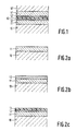
- Fig. 2a shows a substrate 10 of strontium titanate SrTiO3 on which an oxidic superconducting layer 11 of YBa2Cu3O 6.7 is provided, for example, by means of vacuum evaporation, the substrate being maintained at a temperature of 850 o C.
- substrate materials for example MgO, Y2O3 and substrates such as sapphire with protective buffer layers, for example Ta2O5, LaF3 and ZrO2 may also suitably be used in the method according to the invention.
- Substitutions in the superconducting material may be carried out in known manner without affecting the effectiveness of the method according to the invention.
- Y may be completely or partly replaced by rare earth metal ions
- Ba may be replaced by Sr or Ca
- O may be partly replaced by F.
- the invention may be alternatively applied using other oxidic superconducting materials such as Ca-Sr-Bi-Cu oxides, Bi being partly replaceable by Pb, (La, Sr)2CuO4 and cuprates containing Ca and/or Ba in addition to Tl.
- sputtering using a target plate having the desired composition may for example be used instead of vacuum evaporation.
- the substrate is maintained at a high temperature but deposition may also take place at a lower temperature.
- an aftertreatment at a high temperature is required in order to obtain the desired superconducting properties.
- the layer 11 is manufactured by means of dc triode sputtering at a voltage of 1 kV in Ar at a pressure of approximately 0.5 Pa. Subsequently, this layer is subjected to a firing treatment at 700 o to 800 o C in oxygen for approximately 2 hours, as a result of which the layer 11 obtains the appropriate oxygen content and the desired superconducting properties.
- a layer 12 of silver having a thickness of 50 nm, see Fig. 2b, is applied to the layer 11, for example, by means of sputtering. Subsequently, the layers are subjected to a firing treatment at 450 o C in oxygen for 0.5 hours, thus forming a superconducting contact between the silver 12 and the superconducting material 11.
- the surface of the silver layer is converted into silver sulphate Ag2SO4 by a reaction with a gas mixture of H2S and N2 (volume ratio 1 : 4) at room temperature and a pressure of 1 atmosphere for 10 minutes, followed by a post-firing treatment at 350 o C in oxygen for 1 hour. In this manner, a layer 13 of silver sulphate having a thickness of approximately 2 nm is manufactured.
- a second superconducting layer 11′ which is applied to a substrate 10′ and on which a silver layer 12′ is provided, is pressed onto the silver sulphate layer 13 at a temperature of 200 o C and a pressure of approximately 30 N/mm2 in an oxygen atmosphere.
- Fig. 1 shows the Josephson device manufactured in this manner.
- the layers Prior to pressing the two parts of the Josephson device together, the layers may be provided, in known manner, with patterns, for example, by means of photolithographic techniques followed by plasma etching or ion etching.
- the Josephson device may alternatively be manufactured in such a manner that after forming the silver sulphate layer 13 a silver layer 12′ is provided thereon by means of vacuum evaporation after which a superconducting layer 11′ is applied to the latter.
- a Josephson device is manufactured in the manner described in exemplary embodiment 1, with this difference that the silver sulphate layer 13 is manufactured by a reaction of the silver layer 12 with a gas mixture of SO2 and SO3 (volume ratio 1 : 1) at room temperature and atmospheric pressure for 10 minutes.
Applications Claiming Priority (2)
| Application Number | Priority Date | Filing Date | Title |
|---|---|---|---|
| NL8901874 | 1989-07-20 | ||
| NL8901874A NL8901874A (nl) | 1989-07-20 | 1989-07-20 | Planaire josephson inrichting. |
Publications (3)
| Publication Number | Publication Date |
|---|---|
| EP0409338A2 true EP0409338A2 (fr) | 1991-01-23 |
| EP0409338A3 EP0409338A3 (en) | 1991-06-05 |
| EP0409338B1 EP0409338B1 (fr) | 1995-01-25 |
Family
ID=19855071
Family Applications (1)
| Application Number | Title | Priority Date | Filing Date |
|---|---|---|---|
| EP90201922A Expired - Lifetime EP0409338B1 (fr) | 1989-07-20 | 1990-07-16 | Jonction Josephson |
Country Status (7)
| Country | Link |
|---|---|
| US (1) | US5015623A (fr) |
| EP (1) | EP0409338B1 (fr) |
| JP (1) | JPH0358488A (fr) |
| KR (1) | KR910003849A (fr) |
| CN (1) | CN1048950A (fr) |
| DE (1) | DE69016294T2 (fr) |
| NL (1) | NL8901874A (fr) |
Cited By (2)
| Publication number | Priority date | Publication date | Assignee | Title |
|---|---|---|---|---|
| EP0511450A1 (fr) * | 1991-05-01 | 1992-11-04 | International Business Machines Corporation | Dispositif à supraconducteur avec un substrat métallique et procédé pour sa fabrication |
| WO1993001621A1 (fr) * | 1991-07-03 | 1993-01-21 | Cookson Group Plc | Utilisation de sulfates de metaux alcalino-terreux |
Families Citing this family (5)
| Publication number | Priority date | Publication date | Assignee | Title |
|---|---|---|---|---|
| DE69117378T2 (de) * | 1990-07-19 | 1996-09-12 | Sumitomo Electric Industries | Supraleitende Einrichtung mit geschichteter Struktur, zusammengesetzt aus oxidischem Supraleiter und Isolatordünnschicht und deren Herstellungsmethode |
| DE59106363D1 (de) * | 1990-10-26 | 1995-10-05 | Siemens Ag | Verfahren zur Herstellung einer supraleitenden Schicht aus YBa2Cu3O7 auf einem Substrat aus Saphir. |
| JPH04214097A (ja) * | 1990-12-13 | 1992-08-05 | Sumitomo Electric Ind Ltd | 超電導薄膜の作製方法 |
| US7330744B2 (en) * | 2001-11-14 | 2008-02-12 | Nexans | Metal salt resistive layer on an superconducting element |
| US6884527B2 (en) * | 2003-07-21 | 2005-04-26 | The Regents Of The University Of California | Biaxially textured composite substrates |
Citations (1)
| Publication number | Priority date | Publication date | Assignee | Title |
|---|---|---|---|---|
| EP0301675A2 (fr) * | 1987-07-28 | 1989-02-01 | The University of Tokyo | Dispositif supraconducteur et procédé de fabrication |
Family Cites Families (6)
| Publication number | Priority date | Publication date | Assignee | Title |
|---|---|---|---|---|
| JPS63234533A (ja) * | 1987-03-24 | 1988-09-29 | Agency Of Ind Science & Technol | ジヨセフソン接合素子の形成方法 |
| CA1329952C (fr) * | 1987-04-27 | 1994-05-31 | Yoshihiko Imanaka | Substrat pour circuit supraconducteur multicouche et procede de fabrication connexe |
| US4811380A (en) * | 1988-01-29 | 1989-03-07 | Motorola, Inc. | Cellular radiotelephone system with dropped call protection |
| DE3805010A1 (de) * | 1988-02-18 | 1989-08-24 | Kernforschungsanlage Juelich | Verfahren zur herstellung duenner schichten aus oxydischem hochtemperatur-supraleiter |
| JP2644284B2 (ja) * | 1988-05-30 | 1997-08-25 | 株式会社東芝 | 超電導素子 |
| JPH074073B2 (ja) * | 1988-07-04 | 1995-01-18 | 松下電器産業株式会社 | 超音波モータ |
-
1989
- 1989-07-20 NL NL8901874A patent/NL8901874A/nl not_active Application Discontinuation
-
1990
- 1990-07-06 US US07/549,341 patent/US5015623A/en not_active Expired - Fee Related
- 1990-07-16 DE DE69016294T patent/DE69016294T2/de not_active Expired - Fee Related
- 1990-07-16 EP EP90201922A patent/EP0409338B1/fr not_active Expired - Lifetime
- 1990-07-17 CN CN90104605A patent/CN1048950A/zh active Pending
- 1990-07-17 JP JP2187360A patent/JPH0358488A/ja active Pending
- 1990-07-19 KR KR1019900010935A patent/KR910003849A/ko not_active Application Discontinuation
Patent Citations (1)
| Publication number | Priority date | Publication date | Assignee | Title |
|---|---|---|---|---|
| EP0301675A2 (fr) * | 1987-07-28 | 1989-02-01 | The University of Tokyo | Dispositif supraconducteur et procédé de fabrication |
Non-Patent Citations (2)
| Title |
|---|
| APPLIED PHYSICS LETTERS, vol. 54, no. 15, 10th April 1989, pages 1477-1479, New York, US; J. MORELAND et al.: "Evidence for the superconducting proximity effect in junctions between the surfaces of YBa2Cu30x thin films" * |
| IEEE TRANSACTIONS ON MAGNETICS, vol. 25, no. 2, March 1989, pages 1298-1300, New York, US; D.B. SCHWARTZ et al.: "The observation of the AC Josephson effect in a YBa2Cu307/Au/ABa2Cu307 junction" * |
Cited By (4)
| Publication number | Priority date | Publication date | Assignee | Title |
|---|---|---|---|---|
| EP0511450A1 (fr) * | 1991-05-01 | 1992-11-04 | International Business Machines Corporation | Dispositif à supraconducteur avec un substrat métallique et procédé pour sa fabrication |
| US5266558A (en) * | 1991-05-01 | 1993-11-30 | International Business Machines Corporation | Superconducting circuit elements with metallic substrate and method for manufacturing the same |
| US5310706A (en) * | 1991-05-01 | 1994-05-10 | International Business Machines Corporation | Method for manufacturing high Tc superconducting circuit elements with metallic substrate |
| WO1993001621A1 (fr) * | 1991-07-03 | 1993-01-21 | Cookson Group Plc | Utilisation de sulfates de metaux alcalino-terreux |
Also Published As
| Publication number | Publication date |
|---|---|
| KR910003849A (ko) | 1991-02-28 |
| US5015623A (en) | 1991-05-14 |
| EP0409338B1 (fr) | 1995-01-25 |
| CN1048950A (zh) | 1991-01-30 |
| DE69016294T2 (de) | 1995-08-24 |
| NL8901874A (nl) | 1991-02-18 |
| JPH0358488A (ja) | 1991-03-13 |
| DE69016294D1 (de) | 1995-03-09 |
| EP0409338A3 (en) | 1991-06-05 |
Similar Documents
| Publication | Publication Date | Title |
|---|---|---|
| EP0312015B1 (fr) | Substrat en oxyde supraconducteur mis en forme et procédé de fabrication | |
| EP0355888B1 (fr) | Procédé de fabrication d'un dispositif comportant une couche en un matériau supraconducteur à base d'oxyde | |
| US4957899A (en) | Method of patterning superconducting oxide thin films | |
| EP0409338B1 (fr) | Jonction Josephson | |
| EP0336505B1 (fr) | Dispositif et procédé pour la réalisation d'un dispositif | |
| EP0342038B1 (fr) | Dispositif Josephson | |
| US4988672A (en) | Method of forming oxide superconducting layers by solid state diffusion | |
| EP0309273B1 (fr) | Méthode pour produire une couche d'oxyde supraconductrice sur un substrat | |
| EP0358545B1 (fr) | Procédé de fabrication de couches minces supraconductrices du type au thallium | |
| EP0384521A1 (fr) | Procédé pour la fabrication d'une fonction Josephson | |
| JP2667231B2 (ja) | ジョセフソン素子の製造方法 | |
| EP0624910A1 (fr) | Supraconducteur et procédé de fabrication | |
| WO1989003125A1 (fr) | Procede de production d'un circuit electrique contenant des diodes de josephson | |
| EP0333513B1 (fr) | Oxyde supraconducteur | |
| JP2899287B2 (ja) | ジョセフソン素子 | |
| JP3058515B2 (ja) | 超電導ジョセフソン素子およびその製法 | |
| JPH01219023A (ja) | 超伝導体薄膜の製造方法 | |
| JP2685053B2 (ja) | 超伝導複合材料 | |
| JP2776004B2 (ja) | ジョセフソン素子の製造方法 | |
| Donaldson | Fabrication of Tunnel Junction Structures | |
| JPH0246608A (ja) | 超伝導部材用保護膜 | |
| JPH02260676A (ja) | 超電導体装置の製造方法 | |
| JPH07100609B2 (ja) | 薄膜超電導体の製造方法 | |
| JPH01169981A (ja) | 超電導薄膜の製造方法 | |
| JPH01259582A (ja) | 酸化物系超電導薄膜の製造方法 |
Legal Events
| Date | Code | Title | Description |
|---|---|---|---|
| PUAI | Public reference made under article 153(3) epc to a published international application that has entered the european phase |
Free format text: ORIGINAL CODE: 0009012 |
|
| AK | Designated contracting states |
Kind code of ref document: A2 Designated state(s): CH DE FR GB IT LI SE |
|
| PUAL | Search report despatched |
Free format text: ORIGINAL CODE: 0009013 |
|
| AK | Designated contracting states |
Kind code of ref document: A3 Designated state(s): CH DE FR GB IT LI SE |
|
| 17P | Request for examination filed |
Effective date: 19911204 |
|
| 17Q | First examination report despatched |
Effective date: 19940309 |
|
| GRAA | (expected) grant |
Free format text: ORIGINAL CODE: 0009210 |
|
| AK | Designated contracting states |
Kind code of ref document: B1 Designated state(s): CH DE FR GB IT LI SE |
|
| PG25 | Lapsed in a contracting state [announced via postgrant information from national office to epo] |
Ref country code: IT Free format text: LAPSE BECAUSE OF FAILURE TO SUBMIT A TRANSLATION OF THE DESCRIPTION OR TO PAY THE FEE WITHIN THE PRE;WARNING: LAPSES OF ITALIAN PATENTS WITH EFFECTIVE DATE BEFORE 2007 MAY HAVE OCCURRED AT ANY TIME BEFORE 2007. THE CORRECT EFFECTIVE DATE MAY BE DIFFERENT FROM THE ONE RECORDED.SCRIBED TIME-LIMIT Effective date: 19950125 Ref country code: CH Effective date: 19950125 Ref country code: LI Effective date: 19950125 |
|
| REF | Corresponds to: |
Ref document number: 69016294 Country of ref document: DE Date of ref document: 19950309 |
|
| ET | Fr: translation filed | ||
| REG | Reference to a national code |
Ref country code: CH Ref legal event code: PL |
|
| PLBE | No opposition filed within time limit |
Free format text: ORIGINAL CODE: 0009261 |
|
| STAA | Information on the status of an ep patent application or granted ep patent |
Free format text: STATUS: NO OPPOSITION FILED WITHIN TIME LIMIT |
|
| 26N | No opposition filed | ||
| PGFP | Annual fee paid to national office [announced via postgrant information from national office to epo] |
Ref country code: GB Payment date: 19970701 Year of fee payment: 8 |
|
| PGFP | Annual fee paid to national office [announced via postgrant information from national office to epo] |
Ref country code: FR Payment date: 19970722 Year of fee payment: 8 |
|
| PGFP | Annual fee paid to national office [announced via postgrant information from national office to epo] |
Ref country code: SE Payment date: 19970729 Year of fee payment: 8 |
|
| PGFP | Annual fee paid to national office [announced via postgrant information from national office to epo] |
Ref country code: DE Payment date: 19970917 Year of fee payment: 8 |
|
| PG25 | Lapsed in a contracting state [announced via postgrant information from national office to epo] |
Ref country code: GB Free format text: LAPSE BECAUSE OF NON-PAYMENT OF DUE FEES Effective date: 19980716 |
|
| PG25 | Lapsed in a contracting state [announced via postgrant information from national office to epo] |
Ref country code: SE Free format text: LAPSE BECAUSE OF NON-PAYMENT OF DUE FEES Effective date: 19980717 |
|
| REG | Reference to a national code |
Ref country code: FR Ref legal event code: CD |
|
| GBPC | Gb: european patent ceased through non-payment of renewal fee |
Effective date: 19980716 |
|
| EUG | Se: european patent has lapsed |
Ref document number: 90201922.3 |
|
| PG25 | Lapsed in a contracting state [announced via postgrant information from national office to epo] |
Ref country code: FR Free format text: LAPSE BECAUSE OF NON-PAYMENT OF DUE FEES Effective date: 19990331 |
|
| PG25 | Lapsed in a contracting state [announced via postgrant information from national office to epo] |
Ref country code: DE Free format text: LAPSE BECAUSE OF NON-PAYMENT OF DUE FEES Effective date: 19990501 |
|
| REG | Reference to a national code |
Ref country code: FR Ref legal event code: ST |