EP0405952A2 - Halbleiterlasersteuerungskreis - Google Patents
Halbleiterlasersteuerungskreis Download PDFInfo
- Publication number
- EP0405952A2 EP0405952A2 EP90307046A EP90307046A EP0405952A2 EP 0405952 A2 EP0405952 A2 EP 0405952A2 EP 90307046 A EP90307046 A EP 90307046A EP 90307046 A EP90307046 A EP 90307046A EP 0405952 A2 EP0405952 A2 EP 0405952A2
- Authority
- EP
- European Patent Office
- Prior art keywords
- circuit
- laser
- current
- voltage
- control logic
- Prior art date
- Legal status (The legal status is an assumption and is not a legal conclusion. Google has not performed a legal analysis and makes no representation as to the accuracy of the status listed.)
- Granted
Links
Images



Classifications
-
- G—PHYSICS
- G11—INFORMATION STORAGE
- G11B—INFORMATION STORAGE BASED ON RELATIVE MOVEMENT BETWEEN RECORD CARRIER AND TRANSDUCER
- G11B7/00—Recording or reproducing by optical means, e.g. recording using a thermal beam of optical radiation by modifying optical properties or the physical structure, reproducing using an optical beam at lower power by sensing optical properties; Record carriers therefor
- G11B7/12—Heads, e.g. forming of the optical beam spot or modulation of the optical beam
- G11B7/125—Optical beam sources therefor, e.g. laser control circuitry specially adapted for optical storage devices; Modulators, e.g. means for controlling the size or intensity of optical spots or optical traces
- G11B7/126—Circuits, methods or arrangements for laser control or stabilisation
-
- H—ELECTRICITY
- H01—ELECTRIC ELEMENTS
- H01S—DEVICES USING THE PROCESS OF LIGHT AMPLIFICATION BY STIMULATED EMISSION OF RADIATION [LASER] TO AMPLIFY OR GENERATE LIGHT; DEVICES USING STIMULATED EMISSION OF ELECTROMAGNETIC RADIATION IN WAVE RANGES OTHER THAN OPTICAL
- H01S5/00—Semiconductor lasers
- H01S5/06—Arrangements for controlling the laser output parameters, e.g. by operating on the active medium
- H01S5/068—Stabilisation of laser output parameters
- H01S5/06825—Protecting the laser, e.g. during switch-on/off, detection of malfunctioning or degradation
Definitions
- the present invention relates to a semiconductor laser driving circuit which is used in an optical disk recording and reproducing system wherein information is recorded on and reproduced from an optical disk.
- the conventional optical disk system for recording or reproducing information with a laser beam in a recording mode, it serves to follow the steps of intensifying or mitigating a laser output pulsewise in accordance with information to be recorded, changing the power of a laser beam spot restricted on a disk by an optical system accordingly, and changing an optical or magnetic state of a beam-irradiated spot of a recording film formed on the disk for recording the information.
- a reproducing mode it serves to follow the steps of irradiating the disk with a laser beam having such an intensity as not transforming the recording film and detecting the reflected beam for reproducing the information recorded thereon.
- Fig.1 is a circuit diagram showing a conventional laser driving circuit, which mainly includes a control logic circuit 11, a reproduction power producing circuit 12, and a recording power producing circuit 13. Further, it is seen from this figure that a laser 3 and a photodetector 4 are also added to the circuit.
- the photodetector 4 may employ a photodiode.
- the control logic circuit 11 is connected to a +5V power source and the reproduction power producing circuit 12 and the recording power producing circuit 13 are connected to a +12V power source.
- the reproduction power producing circuit 12 includes a transistor 2 for driving the laser 3 in a reproducing mode, a current-to-voltage converting circuit 5 for converting the current generated in the photodetector 4 into a voltage, an operational amplifier 6 for amplifying the converted voltage, and a switching circuit 1 for switching on and off a contact between the operational amplifier 6 and the transistor 2.
- the recording power producing circuit 13 consists of a transistor 9 for driving the laser 3 in a recording mode, a recording power setting circuit 8 connected to the base of transistor 9, and a switching circuit 10 for switching on and off a contact between the transistor 9 and the laser 3.
- the control logic circuit 11 supplies the reproduction signal a to the switching circuit 1, thereby switching on the switching circuit 1 and activating the laser 3. Then, the laser 3 radiates a beam c to the photodetector 4, which generates a current d. Then, the current d is supplied to the current-to-voltage converting circuit 5 in which the current d is converted into a voltage e and is amplified by the operational amplifier 6. The amplified voltage is supplied to the transistor 2 through the switching circuit 1. The transistor 2 serves to adjustably produce the reproduction driving current I R .
- this operation can be summarized as detecting the laser beam and applying negative feedback to the detected signal for keeping a driving current constant.
- the recording power setting circuit 8 supplies a predetermined signal to the transistor 9 in which the recording driving current is adjustably produced, while the control logic circuit 11 supplies the recording signal b to the switching circuit 10.
- the switching circuit 10 is switched on and off in accordance with the magnitude of the signal b.
- the on-and-off switching results in modulating a recording driving current I W and superposing the recording signal on the driving current I W .
- the reproduction driving current I R is kept at the value given immediately before executing the operation in the recording mode by a sample holding circuit (not shown).
- the foregoing semiconductor laser driving circuit has two or more power voltages. That is, the control logic circuit 11 is connected to the +5 power source and the reproduction power producing circuit 12 and the recording power producing circuit 13 are connected to the +12 power source. In this case, the switching of the power sources may result in bringing about a time lag between the leading and the trailing edges of the former power source and those of the latter one.
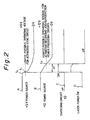
- Fig.2 is a graph showing the state of a voltage caused when the time lag appears, in particular, when the power sources are interrupted in driving the laser.
- the +5v power source connected to the control logic circuit 11 supplies the lowest possible operating voltage for activating the logic circuit 11 at a time t1
- the +12v power source connected to the reproduction power producing circuits 12 and 13 also supplies the lowest possible operating voltage for activating the circuits 12 and 13 at a time t2.
- the control logic circuit 11 cannot keep its logic level stable, thereby switching on the switching circuit 10 as shown in the curve C and supplying the recording driving current I W as shown in the curve D to the laser 3. It results in bringing about a drawback that the laser output reaches such a power that it can transform the recording film formed on the disk and thus gives damage to the information recorded on the disk.
- the invention further provides a means for monitoring the power sources of the semiconductor laser driving circuit, in particular, the power source of the control logic circuit and a means for reducing driving current supplied to the semiconductor laser immediately before or when the source voltage reaches the lowest possible operating value.
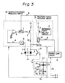
- Fig.3 is a circuit diagram showing a first embodiment of the present invention.
- the embodiment is an improved semiconductor laser driving circuit designed on the foregoing prior art.
- the same components of this embodiment as the prior art are referenced by the same reference notes.
- the improved, that is, different respect of this embodiment from the conventional circuit is that a voltage monitoring circuit 23 is provided in a part of the power source circuit of the control logic circuit 11 and a bypass transistor 21 is connected in parallel to the laser 3.
- the voltage monitoring circuit 23 comprises a Zener diode ZD, a comparator 22 and resistors R1, R2, R3 connected to these former two components.
- the cathode of the Zener diode ZD is connected to the power source of the control logic circuit 11 and a non-inverting input terminal of the comparator 22 through the resistor R3.
- the resistors R3 and R2 connected in series serve as a voltage divider of the source voltage V D so that they reduce the voltage V D to a two-thirds value. Hence, the reduced voltage is applied to the non-inverting input terminal of the comparator 22.
- the other end of the resistor R2 is connected to the ground.
- the anode of the Zener diode ZD is connected to both the inverting input terminal of the comparator 22 and the ground through the resistor R1. It results in making the voltage applied to the inverting input terminal smaller than the source voltage V D by the Zener voltage of 1.5 V.
- Fig.4 is a graph showing the relation among a drop of the source voltage V D , a drop of the voltage applied at the inverting input terminal of the comparator, a drop of the voltage applied at the non-inverting input terminal thereof, a voltage abnormality indicating signal f, and an operating state of the transistor 21 when the power source is interrupted.
- the voltages at the time point are such that the power source voltage V D is equal to 5V
- the non-inverting input terminal voltage is equal to V D ⁇ 2/3 ⁇ 3.3V. After the time t0, these voltages gradually drop.
- the conventional circuit without this invention is incapable of keeping the logic level stable, thereby switching on the switching circuit 10 and allowing the recording driving current I W to be supplied to the laser 3.
- the voltage monitoring circuit 23 serves to monitor a voltage drop and generate the voltage abnormality indicating signal f, thereby causing the transistor 21 to be conductive.
- the transistor 21 is served as a bypass for the recording driving current I W . Since the current I W bypasses the laser 3, the laser is unable to emit a laser beam having such high luminous intensity as being set in the recording mode. It results in preventing the recording film from being damaged by the laser 3.
- Fig.5 is a circuit diagram showing the second embodiment of the present invention, in which the same components of this embodiment as the first one are referenced by the same reference notes. From this figure, it will be understood that a connecting portion of a bypass transistor 21 is different from that of the first embodiment. That is, the collector of the bypass transistor 21 is connected to the emitter of the transistor 9 included in the recording power producing circuit 13. From this connection, when the source voltage V D of the control logic circuit 11 reaches a given voltage or less, therefore, the voltage monitoring circuit 23 serves to supply a high-level signal, thereby causing the transistor 21 to be conductive. Since the transistor 21 serves as a bypass of the recording power producing circuit 13, no excess current is allowed to flow through the laser 3.
Landscapes
- Physics & Mathematics (AREA)
- Optics & Photonics (AREA)
- Condensed Matter Physics & Semiconductors (AREA)
- General Physics & Mathematics (AREA)
- Electromagnetism (AREA)
- Optical Head (AREA)
- Semiconductor Lasers (AREA)
Applications Claiming Priority (2)
| Application Number | Priority Date | Filing Date | Title |
|---|---|---|---|
| JP165577/89 | 1989-06-28 | ||
| JP1165577A JPH0330130A (ja) | 1989-06-28 | 1989-06-28 | 半導体レーザ駆動回路 |
Publications (3)
| Publication Number | Publication Date |
|---|---|
| EP0405952A2 true EP0405952A2 (de) | 1991-01-02 |
| EP0405952A3 EP0405952A3 (en) | 1992-03-04 |
| EP0405952B1 EP0405952B1 (de) | 1995-04-19 |
Family
ID=15815001
Family Applications (1)
| Application Number | Title | Priority Date | Filing Date |
|---|---|---|---|
| EP90307046A Expired - Lifetime EP0405952B1 (de) | 1989-06-28 | 1990-06-27 | Halbleiterlasersteuerungskreis |
Country Status (5)
| Country | Link |
|---|---|
| US (1) | US5170389A (de) |
| EP (1) | EP0405952B1 (de) |
| JP (1) | JPH0330130A (de) |
| CA (1) | CA2019936C (de) |
| DE (1) | DE69018714T2 (de) |
Cited By (2)
| Publication number | Priority date | Publication date | Assignee | Title |
|---|---|---|---|---|
| CN1127185C (zh) * | 1999-05-21 | 2003-11-05 | 北京大学 | 半导体激光器及电吸收调制器的高码率驱动器 |
| WO2004062051A1 (de) * | 2002-12-27 | 2004-07-22 | Osram Opto Semiconductors Gmbh | Laserdiodenbarren mit parallel geschalteter diode zur elektrischen überbrückung des laserdiodenbarrens im fehlerfall |
Families Citing this family (15)
| Publication number | Priority date | Publication date | Assignee | Title |
|---|---|---|---|---|
| JPH0652018U (ja) * | 1992-12-25 | 1994-07-15 | 太陽誘電株式会社 | 光情報記録再生装置 |
| US5422900A (en) * | 1994-04-28 | 1995-06-06 | Eastman Kodak Company | Integrated laser module |
| WO1996020521A1 (en) * | 1994-12-23 | 1996-07-04 | Philips Electronics N.V. | Laser power supply circuit as well as optical recording and/or reading device comprising such a laser power supply circuit |
| JPH1075163A (ja) * | 1996-08-29 | 1998-03-17 | Sony Corp | スイッチ回路 |
| JPH11213425A (ja) * | 1998-01-22 | 1999-08-06 | Olympus Optical Co Ltd | 光ディスク装置 |
| JP2001216646A (ja) | 1999-11-22 | 2001-08-10 | Sanyo Electric Co Ltd | データ記録装置 |
| JP3594547B2 (ja) | 1999-11-22 | 2004-12-02 | 三洋電機株式会社 | データ記録装置 |
| JP2001216645A (ja) | 1999-11-22 | 2001-08-10 | Sanyo Electric Co Ltd | 制御装置 |
| JP2001216647A (ja) * | 1999-11-22 | 2001-08-10 | Sanyo Electric Co Ltd | 制御装置 |
| JP2001250329A (ja) * | 1999-12-27 | 2001-09-14 | Sanyo Electric Co Ltd | データ記録装置 |
| JP3754288B2 (ja) * | 1999-12-27 | 2006-03-08 | 三洋電機株式会社 | 制御装置 |
| JP3545330B2 (ja) | 1999-12-27 | 2004-07-21 | 三洋電機株式会社 | 記録制御装置 |
| JP2001250327A (ja) * | 1999-12-27 | 2001-09-14 | Sanyo Electric Co Ltd | データ記録システム |
| TW473705B (en) * | 2000-01-28 | 2002-01-21 | Via Tech Inc | Method and device to prevent overcurrent of pickup head |
| KR100464403B1 (ko) * | 2001-07-20 | 2005-01-03 | 삼성전자주식회사 | 광디스크 기록/재생 장치의 이상 상태 검출 장치 |
Family Cites Families (9)
| Publication number | Priority date | Publication date | Assignee | Title |
|---|---|---|---|---|
| JPS56144590A (en) * | 1980-04-13 | 1981-11-10 | Matsushita Electric Ind Co Ltd | Driving device for semiconductor laser |
| JPS5894143A (ja) * | 1981-12-01 | 1983-06-04 | Matsushita Electric Ind Co Ltd | 光学的記録再生装置 |
| JPS6190539A (ja) * | 1984-10-09 | 1986-05-08 | Olympus Optical Co Ltd | 光出力安定化装置 |
| JP2563250B2 (ja) * | 1985-06-17 | 1996-12-11 | 松下電器産業株式会社 | 半導体レ−ザ駆動回路 |
| US4685097A (en) * | 1985-07-25 | 1987-08-04 | Laser Magnetic Storage International Company | Power control system for a semiconductor laser |
| JPS62102576A (ja) * | 1985-10-29 | 1987-05-13 | Toshiba Corp | レ−ザダイオ−ド駆動回路のリセツト回路 |
| DE3688276T2 (de) * | 1985-10-16 | 1993-07-29 | Sharp Kk | Steuervorrichtung des buendels fuer magnetooptisches plattenspeichersystem. |
| JP2615553B2 (ja) * | 1985-11-14 | 1997-05-28 | 富士通株式会社 | レーザ制御装置 |
| JPH07111782B2 (ja) * | 1986-08-13 | 1995-11-29 | ソニー株式会社 | 光デイスクの記録再生装置 |
-
1989
- 1989-06-28 JP JP1165577A patent/JPH0330130A/ja active Pending
-
1990
- 1990-06-15 US US07/538,340 patent/US5170389A/en not_active Expired - Lifetime
- 1990-06-27 CA CA002019936A patent/CA2019936C/en not_active Expired - Fee Related
- 1990-06-27 EP EP90307046A patent/EP0405952B1/de not_active Expired - Lifetime
- 1990-06-27 DE DE69018714T patent/DE69018714T2/de not_active Expired - Lifetime
Cited By (2)
| Publication number | Priority date | Publication date | Assignee | Title |
|---|---|---|---|---|
| CN1127185C (zh) * | 1999-05-21 | 2003-11-05 | 北京大学 | 半导体激光器及电吸收调制器的高码率驱动器 |
| WO2004062051A1 (de) * | 2002-12-27 | 2004-07-22 | Osram Opto Semiconductors Gmbh | Laserdiodenbarren mit parallel geschalteter diode zur elektrischen überbrückung des laserdiodenbarrens im fehlerfall |
Also Published As
| Publication number | Publication date |
|---|---|
| DE69018714D1 (de) | 1995-05-24 |
| CA2019936A1 (en) | 1990-12-28 |
| DE69018714T2 (de) | 1995-10-05 |
| CA2019936C (en) | 1994-08-23 |
| US5170389A (en) | 1992-12-08 |
| EP0405952A3 (en) | 1992-03-04 |
| EP0405952B1 (de) | 1995-04-19 |
| JPH0330130A (ja) | 1991-02-08 |
Similar Documents
| Publication | Publication Date | Title |
|---|---|---|
| EP0405952B1 (de) | Halbleiterlasersteuerungskreis | |
| EP0169579B1 (de) | Steuerschaltung für einen Halbleiterlaser | |
| US4713819A (en) | Semiconductor laser driver | |
| US6563848B1 (en) | Semiconductor laser drive device | |
| JPH1064069A (ja) | 光記録再生装置 | |
| EP0469929B1 (de) | Steuerung von Strömen in Laserdioden | |
| KR950013056B1 (ko) | 레이져 다이오드 제어장치 | |
| US5260956A (en) | Laser drive circuit | |
| US5008888A (en) | Semiconductor laser driving apparatus | |
| US4718068A (en) | Stabilized laser device of optical information recording/reproduction apparatus | |
| JP3034485B2 (ja) | 自動レーザー出力制御回路 | |
| US5831959A (en) | Laser control circuit in recordable optical disk drive | |
| US5660474A (en) | Temperature detecting circuit generating an output signal according to the temperature | |
| US20030099178A1 (en) | Optical disc drive and laser beam drive power supply voltage control method | |
| EP0402081B1 (de) | Aufzeichnungs- und Wiedergabegerät für optische Daten | |
| JP2563250B2 (ja) | 半導体レ−ザ駆動回路 | |
| JP3001016B2 (ja) | 半導体レーザ駆動装置 | |
| EP0436939B1 (de) | Datenwiedergabegerät für optische Platte | |
| JPH0722562U (ja) | 半導体レーザ制御回路 | |
| KR960019118A (ko) | 광 기록·재생 장치의 레이저 파워 제어 회로 및 그 제어 방법 | |
| US5303222A (en) | Optical record reproducing apparatus including automatic light amount control | |
| JPH0718019Y2 (ja) | 発光手段ドライブ回路 | |
| JP2001331960A (ja) | 光ディスク装置 | |
| JP2734050B2 (ja) | 半導体レーザ駆動回路 | |
| JPH038133A (ja) | 光学式データ記憶再生装置 |
Legal Events
| Date | Code | Title | Description |
|---|---|---|---|
| PUAI | Public reference made under article 153(3) epc to a published international application that has entered the european phase |
Free format text: ORIGINAL CODE: 0009012 |
|
| AK | Designated contracting states |
Kind code of ref document: A2 Designated state(s): DE FR GB IT NL |
|
| 17P | Request for examination filed |
Effective date: 19901220 |
|
| PUAL | Search report despatched |
Free format text: ORIGINAL CODE: 0009013 |
|
| AK | Designated contracting states |
Kind code of ref document: A3 Designated state(s): DE FR GB IT NL |
|
| 17Q | First examination report despatched |
Effective date: 19931022 |
|
| GRAA | (expected) grant |
Free format text: ORIGINAL CODE: 0009210 |
|
| AK | Designated contracting states |
Kind code of ref document: B1 Designated state(s): DE FR GB IT NL |
|
| REF | Corresponds to: |
Ref document number: 69018714 Country of ref document: DE Date of ref document: 19950524 |
|
| ITF | It: translation for a ep patent filed | ||
| ET | Fr: translation filed | ||
| PLBE | No opposition filed within time limit |
Free format text: ORIGINAL CODE: 0009261 |
|
| STAA | Information on the status of an ep patent application or granted ep patent |
Free format text: STATUS: NO OPPOSITION FILED WITHIN TIME LIMIT |
|
| 26N | No opposition filed | ||
| REG | Reference to a national code |
Ref country code: GB Ref legal event code: IF02 |
|
| PGFP | Annual fee paid to national office [announced via postgrant information from national office to epo] |
Ref country code: NL Payment date: 20060615 Year of fee payment: 17 |
|
| PGFP | Annual fee paid to national office [announced via postgrant information from national office to epo] |
Ref country code: IT Payment date: 20060630 Year of fee payment: 17 |
|
| NLV4 | Nl: lapsed or anulled due to non-payment of the annual fee |
Effective date: 20080101 |
|
| PG25 | Lapsed in a contracting state [announced via postgrant information from national office to epo] |
Ref country code: NL Free format text: LAPSE BECAUSE OF NON-PAYMENT OF DUE FEES Effective date: 20080101 |
|
| PG25 | Lapsed in a contracting state [announced via postgrant information from national office to epo] |
Ref country code: IT Free format text: LAPSE BECAUSE OF NON-PAYMENT OF DUE FEES Effective date: 20070627 |
|
| PGFP | Annual fee paid to national office [announced via postgrant information from national office to epo] |
Ref country code: GB Payment date: 20090624 Year of fee payment: 20 Ref country code: DE Payment date: 20090626 Year of fee payment: 20 |
|
| REG | Reference to a national code |
Ref country code: GB Ref legal event code: PE20 Expiry date: 20100626 |
|
| PG25 | Lapsed in a contracting state [announced via postgrant information from national office to epo] |
Ref country code: GB Free format text: LAPSE BECAUSE OF EXPIRATION OF PROTECTION Effective date: 20100626 |
|
| PG25 | Lapsed in a contracting state [announced via postgrant information from national office to epo] |
Ref country code: DE Free format text: LAPSE BECAUSE OF EXPIRATION OF PROTECTION Effective date: 20100627 |
|
| PGFP | Annual fee paid to national office [announced via postgrant information from national office to epo] |
Ref country code: FR Payment date: 20090611 Year of fee payment: 20 |