EP0403274A1 - Integrierte Kundenwunschschaltungsvorrichtung - Google Patents
Integrierte Kundenwunschschaltungsvorrichtung Download PDFInfo
- Publication number
- EP0403274A1 EP0403274A1 EP90306479A EP90306479A EP0403274A1 EP 0403274 A1 EP0403274 A1 EP 0403274A1 EP 90306479 A EP90306479 A EP 90306479A EP 90306479 A EP90306479 A EP 90306479A EP 0403274 A1 EP0403274 A1 EP 0403274A1
- Authority
- EP
- European Patent Office
- Prior art keywords
- unit
- transistor
- resistor
- capacitor
- type region
- Prior art date
- Legal status (The legal status is an assumption and is not a legal conclusion. Google has not performed a legal analysis and makes no representation as to the accuracy of the status listed.)
- Granted
Links
Images


Classifications
-
- H—ELECTRICITY
- H10—SEMICONDUCTOR DEVICES; ELECTRIC SOLID-STATE DEVICES NOT OTHERWISE PROVIDED FOR
- H10D—INORGANIC ELECTRIC SEMICONDUCTOR DEVICES
- H10D84/00—Integrated devices formed in or on semiconductor substrates that comprise only semiconducting layers, e.g. on Si wafers or on GaAs-on-Si wafers
- H10D84/90—Masterslice integrated circuits
- H10D84/903—Masterslice integrated circuits comprising field effect technology
- H10D84/907—CMOS gate arrays
-
- H—ELECTRICITY
- H10—SEMICONDUCTOR DEVICES; ELECTRIC SOLID-STATE DEVICES NOT OTHERWISE PROVIDED FOR
- H10D—INORGANIC ELECTRIC SEMICONDUCTOR DEVICES
- H10D84/00—Integrated devices formed in or on semiconductor substrates that comprise only semiconducting layers, e.g. on Si wafers or on GaAs-on-Si wafers
- H10D84/90—Masterslice integrated circuits
Definitions
- the present invention relates to a semi-custom integrated circuit apparatus capable of discretionally forming a gate array of a digital circuit (logic circuit), a gate array of an analog circuit, or a gate array on which a digital circuit and an analog circuit are mixed.
- a gate array on which a logic circuit is provided forms the main current. Furthermore, in a recently developed device, a gate array on which an analog circuit is provided has both a digital circuit and an analog circuit formed on the gate array.
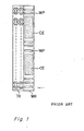
- Figure 1 represents a plan view of a main part of a cell array in a semi-custom IC disclosed in this Japanese Patent Disclosure.
- TR represents a transistor region, WR a wiring region, WP a wiring poly-silicon film and CE a capacitor poly-silicon film.
- respective cells In a semi-custom integrated circuit, respective cells must have a rectangular shape to enable the arrangement and wiring to be designed by a computer. Respective regions with a bulk form are fixed. Only the wiring is changed to enable the device to be provided with different functions.
- the prior art invention disclosed in the above patent disclosure is limited to the idea in which a digital circuit and an analog circuit are merely mixed. Therefore, in this prior art, the arrangement of the resistor and capacitor is not regular. Thus, it requires an unnecessarily large space, thereby drastically decreasing the number of cells with an analog function which can be provided in the cell. In particular, this prior art does not clearly specify the wiring and thus does not solve the wiring problem. Thus, as can be seen from the above, the prior art has serious problems which may make it impossible to realize a gate array on which a digital circuit and analog circuit can be mixedly mounted.
- An object of the present invention is to provide a semi-custom integrated circuit device capable of mounting a digital circuit and an analog circuit either independently or in a mixed manner. This is achieved by forming a basic cell with a combination of a transistor unit, a resistor unit and a capacitor unit.
- a feature of the present invention resides in a semi-custom integrated circuit comprising a basic cell array comprising a plurality of basic cells aligned in a first direction, each of the basic cells comprising a transistor unit, a capacitor unit and a resistor unit arranged in a second direction perpendicular to the first direction, the transistor unit being positioned between the capacitor unit and the resistor unit, the transistor unit having a terminal portion for connection of wiring, the capacitor unit having a terminal portion for connection of wiring, the resistor unit having a terminal portion for connection of wiring, and the terminal portions of the transistor unit, capacitor unit and resistor unit being aligned along a line.
- a plurality of said cell arrays are arranged in a second direction crossing a wiring region.
- an unused region on the capacitor unit or transistor unit is used for the arrangement of an interconnection wiring between said basic cells.
- the transistor unit comprises a source region and a drain region arranged in the first direction, a gate electrode provided between the source region and drain region and extending in the second direction, and the gate electrode having terminal portions in the terminal region.
- the resistor unit comprises a polysilicon layer formed on an insulating film covering a semiconductor substrate and extending in the second direction and having a terminal portion
- the capacitor unit comprising a first electrode formed on the insulating film for covering the semiconductor substrate, an insulating film for covering a first electrode and a second electrode formed on the insulating film, the first and second electrodes having respective terminal portions.
- the transistor unit comprises a p-channel MIS- transistor pair and an n-channel MIS-transistor pair arranged in the second direction
- the p-channel MIS transistor pair comprises a first p-type region a second p-type region, and a third p-type region, which are arranged in the first direction, a first gate electrode arranged between the first p-type region and the second p-type region and extended in the second direction and the second gate region arranged between the second p-type region and the third p-type region and extended in the second direction
- the n-channel MIS transistor pair comprises a first n-type region a second n-type region, a third n-type region, which are arranged in the first direction, a third gate electrode arranged between the first n-type region and the second n-type region and extended in the second direction, and a fourth gate electrode arranged in the second n-type region and the third n-type region and extended in the second direction
- the resistor
- the first and third gate electrodes are formed of an integrated electrode and the second and fourth electrodes are formed of an integrated electrode.
- the transistor unit comprises first and second p-channel MIS transistor pairs and first and second n-channel MIS transistor pairs arranged in the second direction, the first and second p-channel MIS transistor pairs each comprise a first p-type region, a second p-type region and a third p-type region arranged in the first direction, a first gate electrode arranged between the first p-type region and the second p-type region and extended in the second direction, and a second gate electrode arranged between the second p-type region and the third p-type region and extended in the second direction, the first and second n-channel MIS transistor pair each having a first n-type region, a second n-type region and a third n-type region arranged in the first direction, a third gate region arranged between the first n-type region and the second n-type region and extended in the second direction, and a fourth gate electrode arranged between the second n-type region and the third n-type region and extended in the second direction
- the first and second p-channel MIS transistor pair or said first and second n-channel MIS transistor pair are arranged adjacent to each other.
- a plurality of the transistor units forms a digital circuit through an interconnection and a plurality of resistor units and capacitor units forms an analog circuit through an internal connection.
- Figures 2A and 2B respectively, show a plan view of a main part of a basic cell for explaining the principle of the present invention and equivalent circuit thereof.
- 1 is a transistor unit, 1p a p-channel transistor portion, 1n an n-channel transistor portion, 2 a resistor unit, 3 a capacitor unit, ST the width of the transistor unit 1, SR the width of the resistor unit 2, and SC the width of the capacitor unit 3.
- transistor unit 1 As described above, in the present invention, transistor unit 1, resistor unit 2, and capacitor unit 3 are combined to form a single basic cell and the basic cell is arranged as an array.
- the basic cell shown in Figure 2A provides resistor unit 2 on the left side of transistor unit 1 and capacitor unit 3 on the right side thereof.
- the structure of the basic cell can be modified in various ways and the arrangement of the basic cell can be selected appropriately as necessary.
- the number of transistors may be one or more than one.
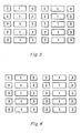
- Figure 3 represents an array in which the basic cell shown in Figure 2A is sequentially arranged.
- Figure 4 represents an array of a basic cell in which the positions of the capacitor unit 3 and resistor unit 2 are exchanged with those of the resistor unit 2 and capacitor unit 3 of the basic cell shown in Figure 3, such array of the basic cell being provided in one column.
- the array of the basic cell shown in Figure 3 is provided in the adjacent column.
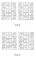
- Figure 5 represents an array in which the basic cell shown in Figure 3 and the basic cell shown in Figure 4 are provided in turn.
- Figure 6 shows an array in which a basic cell having resistor units 2 provided on both sides of the transistor unit 1 and a basic cell having capacitor units 3 provided on both sides of the transistor unit 1 are arranged in turn and the basic cell array on the left side is shifted from the basic cell array on the right side by one basic cell.
- Figure 7 represents an array in which the basic cell array on the left side becomes the same basic cell array on the right side in the array relationship shown in Figure 6.
- the width ST of the transistor unit 1 is equal to the width ST of resistor unit 2 and the width SC of capacitor unit 3, but the widths ST, SR and SC can be properly selected within a scope facilitating a computer aided design.
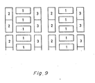
- Figures 8 and 9 are an explanatory main part plan views relating to an array for explaining a case in which the width SR of resistor unit 2 and the width SC of capacitor unit 3 are not equal to the width ST of transistor unit 1.
- the width SR of the resistor unit 2 and the width SC of the capacitor unit 3 are a positive integer times the width ST the of transistor unit 1.
- Figure 9 represents an array in which the width SR of resistor unit 2 and the width SC of capacitor unit 3 are a positive integer times half the width ST of the transistor unit 1.
- the basic cell forms the transistor unit 1 in the transistor area TR and forms the resistor unit 2 and capacitor unit 3 so that they are buried in the wiring region WR.
- the gate array is of a channelless type (i.e. a sea of gate: SOG), the basic cell is provided over the entire area.
- a resistor unit for example, the resistor unit 2 or capacitor unit (for example, the capacitor unit 3) is provided on both sides of a transistor unit (for example, the transistor unit 1).
- the vertical width of these units is either the same as the vertical width (for example, the width ST) of the transistor unit, a positive integer times the vertical width of the transistor unit or positive integer times half the vertical width of the transistor unit.
- This assembly forms a basic cell.
- a transistor unit may be provided in the transistor region and the resistor or capacitor units may be provided in the wiring region provided beside the transistor region.
- FIGS 10A and 10B 11 to 32 indicate terminals, R1 and R2 resistors, QP1 and QP2 p-channel and QN2 n-channel transistors, QP3 and QP4 q-channel transistors, QN3 and QN4 n-channel transistors, C1 a capacitor, CP a contact pattern for connection to a p-type substrate and CN a contact pattern for connection to an n-type substrate.
- Respective transistors in Figures 10A and 10B are represented by their gates and symbols are given to their gates.
- An impurity diffused region R1 of the resistor unit 2 is to form a resistor R1.
- the regions 11 and 13 are to for terminals 11 and 13 of the resistor R1.
- Regions 16 and 21 are to form gate terminals 16 and 21 of the transistors QP1 and QP2.
- Regions 15 and 20 are to form source terminals 15 and 20.
- Region 18 is to form drain electrode 18.
- Regions 31 and 32 are to form terminal 31 and 32 of capacitor C1.
- the regions for terminals 11,13, 16 and 24 are aligned with each other.
- the regions for terminals 12,14, 21, 29 and 32 are alinged with each other. Therefore terminals of the resistor unit 2, transistor unit 1 and capacitor unit 3 are aligned with each other in a horizontal direction, for example, analog a line of a grid (not shown).
- Contact patterns CN and CP are also aligned in a horizontal direction. Some of the terminals or contact patterns may be aligned in a vertical direction. Therefore, the embodiment shown in Figure 10A facilitates computer aided design and wiring.
- Figure 11 is a sectional view of a main part along the line Y1-Y1 shown in Figure 10A and the same reference numbers as in Figures 2 and 10A represent the same parts as in Figures 2 to 10A.
- 41 indicates an n type semiconductor substrate
- 42 a field insulating film comprising a silicon dioxide (Sio2)
- 43A and 43B are p-type resistor regions
- 44 an insulating film formed simultaneously with a gate insulating film.
- Figure 12 is a sectional view of the main part along the line x-x shown in Figure 10A and the same references as used in Figure 2 to 11 represent the same parts or the same meanings.
- Figure 13 is a sectional view of the main part along the line Y2-Y2 shown in Figure 10A.
- the same reference numbers as used Figures 2 to 12 represent the same parts or the same meanings.
- 48 indicates a polisilicon gate electrode of transistor QP1, 49 a polisilicon gate electrode of transistor QP2, 50 a p-type source region of transistor QP1 and QP2, 51 a p-type drain region of transistors Q1, 52 a p-type drain region of transistor AP2, and 53 a between-layer insulating film comprising Sio2.
- Figure 14 is a sectional view of the main part along the line Y-3 shown in Figure 10A.
- the same reference numbers as in Figures 2 to 13 represent the same parts or the same meanings.
- 54 indicates a p-type region, 55 a capacitor electrode of polysilicon, 56 a capacitor dielectric film comprising Sio2, 57 a capacitor electrode of a polysilicon and 58 an insulating film.
- Figures 15 and 16 represent a plan view of the main part for explaining the pattern layout of an operational amplifier formed by and the equivalent circuit diagram the basic cell of the present invention.
- the reference numbers as used in Figures 1 to 13 represent the same parts or the same meanings.
- V DD represents a positive power source level
- Vss a ground side power source level
- IM a -difference input IP a +difference input
- VR a bias input VR a bias input
- OT an output.
- the wire represented by a solid line is made of metal wire and it is in the first layer Al.
- the wire represented by a dashed line is also made of metal and is in the second layer Al.
- the x mark indicates the contact portion between the first-layer metal wire and the bulk, and the O mark designates the contact point between the first-layer metal wire and the second-layer metal wire.
- Transistor unit 1 resistor unit 2 and capacitor unit 3 can be wired by computer-aided automatic design.
- Figure 17 is an explanatory plan view of the main part representing the whole bulk for explaining a gate array embodying the present invention.
- the same reference numbers used in Figures 2 to 16 represent the same portions or the same meanings.
- BR represents an input and output buffer and BP an input and output bonding pad.
- resistor unit 2 and capacitor unit 3 in the basic cell need not be used. Further more, if the gate array is used only for an analog circuit, the whole basic cell can be used. If they are selectively embodied, a gate array in which a logic circuit and an analog circuit are mixed can be realized. When the gate array is formed only by the logic circuit, it does not cause any problem even if a metal wire passes over resistor unit 2 or capacitor unit 3.
- the basic cell of the present invention can also form A/D or D/A converter, analog switch, and comparator, for example.
- the basic cell of the present invention may be used for a full-custom integrated circuit device and a regular standard integrated circuit device.
- a resistor unit or a capacitor unit are provided on both sides of the transistor unit to form a basic array.
- the vertical width of these units is either the same as that of the transistor unit, a positive integer times the vertical width of the transistor unit, or a positive integer times half the vertical width of the transistor unit.
- the transistor unit may be provided on the transistor region and the resistor unit or capacitor unit may be provided on the region formed beside the transistor region.
- the digital circuit and the analog circuit can be independently or mixedly mounted, thereby providing semiconductor integration.
- the wiring required to complete an integrated circuit device to be provided to a user can be dealt with by automatic computer aided design using the conventional technology.
Landscapes
- Design And Manufacture Of Integrated Circuits (AREA)
- Semiconductor Integrated Circuits (AREA)
Applications Claiming Priority (2)
| Application Number | Priority Date | Filing Date | Title |
|---|---|---|---|
| JP1149473A JP3030778B2 (ja) | 1989-06-14 | 1989-06-14 | セミカスタム集積回路装置 |
| JP149473/89 | 1989-06-14 |
Publications (2)
| Publication Number | Publication Date |
|---|---|
| EP0403274A1 true EP0403274A1 (de) | 1990-12-19 |
| EP0403274B1 EP0403274B1 (de) | 1994-10-12 |
Family
ID=15475914
Family Applications (1)
| Application Number | Title | Priority Date | Filing Date |
|---|---|---|---|
| EP90306479A Expired - Lifetime EP0403274B1 (de) | 1989-06-14 | 1990-06-14 | Integrierte Kundenwunschschaltungsvorrichtung |
Country Status (4)
| Country | Link |
|---|---|
| EP (1) | EP0403274B1 (de) |
| JP (1) | JP3030778B2 (de) |
| KR (1) | KR930006985B1 (de) |
| DE (1) | DE69013235T2 (de) |
Families Citing this family (2)
| Publication number | Priority date | Publication date | Assignee | Title |
|---|---|---|---|---|
| KR101259751B1 (ko) * | 2008-09-08 | 2013-04-30 | 삼성전자주식회사 | 액티브 저항의 길이와 같은 너비를 갖는 커패시터를 포함하는 반도체 집적 회로의 배치 방법 |
| JP6045923B2 (ja) * | 2013-01-25 | 2016-12-14 | レンゴー株式会社 | 仕切材 |
Citations (1)
| Publication number | Priority date | Publication date | Assignee | Title |
|---|---|---|---|---|
| EP0189183A1 (de) * | 1985-01-25 | 1986-07-30 | Hitachi, Ltd. | Integrierte Halbleiterschaltungsanordnung |
Family Cites Families (5)
| Publication number | Priority date | Publication date | Assignee | Title |
|---|---|---|---|---|
| JPS6390844U (de) * | 1986-12-04 | 1988-06-13 | ||
| JPS63142656A (ja) * | 1986-12-05 | 1988-06-15 | Fuji Xerox Co Ltd | セミカスタム半導体集積回路 |
| JPS647536A (en) * | 1987-06-29 | 1989-01-11 | Nec Corp | Semi-custom semiconductor integrated circuit |
| JPH01123432A (ja) * | 1987-11-09 | 1989-05-16 | Nec Corp | 半導体集積回路装置 |
| JPH01248535A (ja) * | 1988-03-29 | 1989-10-04 | Nec Corp | セミカスタム集積回路 |
-
1989
- 1989-06-14 JP JP1149473A patent/JP3030778B2/ja not_active Expired - Fee Related
-
1990
- 1990-06-14 KR KR9008726A patent/KR930006985B1/ko not_active Expired - Fee Related
- 1990-06-14 EP EP90306479A patent/EP0403274B1/de not_active Expired - Lifetime
- 1990-06-14 DE DE69013235T patent/DE69013235T2/de not_active Expired - Fee Related
Patent Citations (1)
| Publication number | Priority date | Publication date | Assignee | Title |
|---|---|---|---|---|
| EP0189183A1 (de) * | 1985-01-25 | 1986-07-30 | Hitachi, Ltd. | Integrierte Halbleiterschaltungsanordnung |
Non-Patent Citations (3)
| Title |
|---|
| PATENT ABSTRACTS OF JAPAN, vol. 10, no. 99 (E-396)[2156], 16th April 1986; & JP-A-60 240 139 (SUMITOMO DENKI KOGYO K.K.) 29-11-1985 * |
| PATENT ABSTRACTS OF JAPAN, vol. 9, no. 136 (E-320)[1859], 12th June 1985; & JP-A-60 18 932 (SUWA SEIKOSHA K.K.) 31-01-1985 * |
| PATENT ABSTRACTS OF JAPAN, vol. 9, no. 201 (E-336)[1924] 17th August 1985; & JP-A-60 66 449 (SUWA SEIKOSHA K.K.) 16-04-1985 * |
Also Published As
| Publication number | Publication date |
|---|---|
| JPH0316173A (ja) | 1991-01-24 |
| KR930006985B1 (en) | 1993-07-24 |
| EP0403274B1 (de) | 1994-10-12 |
| DE69013235T2 (de) | 1995-02-23 |
| JP3030778B2 (ja) | 2000-04-10 |
| DE69013235D1 (de) | 1994-11-17 |
Similar Documents
| Publication | Publication Date | Title |
|---|---|---|
| EP0058504B1 (de) | Verfahren zur Herstellung eines Verzögerungsgliedes in einer integrierten "Master-Slice"-Schaltung | |
| JP3154411B2 (ja) | Cadによってレイアウトされた2金属層集積回路ゲート・アレイ | |
| KR920004179B1 (ko) | 반도체집적회로 | |
| US5663589A (en) | Current regulating semiconductor integrated circuit device and fabrication method of the same | |
| EP0080361B1 (de) | Komplementaire Metalloxidhalbleiter enthaltende integrierte Schaltungsvorrichtung in Mutterscheibentechnik | |
| US5087955A (en) | Input-output circuit of reduced device area for semicustom semiconductor integrated circuit | |
| US5300796A (en) | Semiconductor device having an internal cell array region and a peripheral region surrounding the internal cell array for providing input/output basic cells | |
| US4525809A (en) | Integrated circuit | |
| US4750027A (en) | Master slice semiconductor device | |
| US4771327A (en) | Master-slice integrated circuit having an improved arrangement of transistor elements for simplified wirings | |
| JPS6065547A (ja) | 半導体装置 | |
| US4524377A (en) | Integrated circuit | |
| US5281835A (en) | Semi-custom integrated circuit device | |
| US5952698A (en) | Layout pattern for improved MOS device matching | |
| EP0403274B1 (de) | Integrierte Kundenwunschschaltungsvorrichtung | |
| EP0650196A2 (de) | Integrierte Halbleiterschaltungsanordnung vom Masterslice-Typ und Herstellungsverfahren dafür | |
| JP2997179B2 (ja) | パワーmosトランジスタ | |
| JPS586157A (ja) | Cmosマスタ・スライスlsi | |
| JP2000223575A (ja) | 半導体装置の設計方法、半導体装置および半導体装置の製造方法 | |
| US6081004A (en) | BiCMOS compacted logic array | |
| EP0136888B1 (de) | Hochintegrierte Schaltung | |
| KR100211768B1 (ko) | 삼중 금속층을 가지는 반도체 메모리 장치 | |
| EP1009031B1 (de) | Integriertes Halbleiterschaltkreisbauelement und dessen Herstellungsverfahren | |
| EP0730303A2 (de) | Mikroelektronische integrierte Schaltung mit hexagonalem CMOS-"NAND"-Tor | |
| HK28196A (en) | I/O cells in semiconductor integrated circuits |
Legal Events
| Date | Code | Title | Description |
|---|---|---|---|
| PUAI | Public reference made under article 153(3) epc to a published international application that has entered the european phase |
Free format text: ORIGINAL CODE: 0009012 |
|
| AK | Designated contracting states |
Kind code of ref document: A1 Designated state(s): DE FR GB |
|
| 17P | Request for examination filed |
Effective date: 19910507 |
|
| 17Q | First examination report despatched |
Effective date: 19930115 |
|
| GRAA | (expected) grant |
Free format text: ORIGINAL CODE: 0009210 |
|
| AK | Designated contracting states |
Kind code of ref document: B1 Designated state(s): DE FR GB |
|
| REF | Corresponds to: |
Ref document number: 69013235 Country of ref document: DE Date of ref document: 19941117 |
|
| ET | Fr: translation filed | ||
| PLBE | No opposition filed within time limit |
Free format text: ORIGINAL CODE: 0009261 |
|
| STAA | Information on the status of an ep patent application or granted ep patent |
Free format text: STATUS: NO OPPOSITION FILED WITHIN TIME LIMIT |
|
| 26N | No opposition filed | ||
| REG | Reference to a national code |
Ref country code: GB Ref legal event code: IF02 |
|
| PGFP | Annual fee paid to national office [announced via postgrant information from national office to epo] |
Ref country code: GB Payment date: 20050608 Year of fee payment: 16 Ref country code: FR Payment date: 20050608 Year of fee payment: 16 |
|
| PGFP | Annual fee paid to national office [announced via postgrant information from national office to epo] |
Ref country code: DE Payment date: 20050609 Year of fee payment: 16 |
|
| PG25 | Lapsed in a contracting state [announced via postgrant information from national office to epo] |
Ref country code: GB Free format text: LAPSE BECAUSE OF NON-PAYMENT OF DUE FEES Effective date: 20060614 |
|
| PG25 | Lapsed in a contracting state [announced via postgrant information from national office to epo] |
Ref country code: DE Free format text: LAPSE BECAUSE OF NON-PAYMENT OF DUE FEES Effective date: 20070103 |
|
| GBPC | Gb: european patent ceased through non-payment of renewal fee |
Effective date: 20060614 |
|
| REG | Reference to a national code |
Ref country code: FR Ref legal event code: ST Effective date: 20070228 |
|
| PG25 | Lapsed in a contracting state [announced via postgrant information from national office to epo] |
Ref country code: FR Free format text: LAPSE BECAUSE OF NON-PAYMENT OF DUE FEES Effective date: 20060630 |