EP0189183A1 - Integrierte Halbleiterschaltungsanordnung - Google Patents
Integrierte Halbleiterschaltungsanordnung Download PDFInfo
- Publication number
- EP0189183A1 EP0189183A1 EP86100798A EP86100798A EP0189183A1 EP 0189183 A1 EP0189183 A1 EP 0189183A1 EP 86100798 A EP86100798 A EP 86100798A EP 86100798 A EP86100798 A EP 86100798A EP 0189183 A1 EP0189183 A1 EP 0189183A1
- Authority
- EP
- European Patent Office
- Prior art keywords
- basic
- basic cell
- cell
- cells
- integrated circuit
- Prior art date
- Legal status (The legal status is an assumption and is not a legal conclusion. Google has not performed a legal analysis and makes no representation as to the accuracy of the status listed.)
- Granted
Links
- 239000004065 semiconductor Substances 0.000 claims abstract description 23
- 238000003491 array Methods 0.000 claims description 27
- 239000000758 substrate Substances 0.000 claims description 7
- 239000002131 composite material Substances 0.000 claims description 6
- 239000000470 constituent Substances 0.000 claims description 5
- 230000005669 field effect Effects 0.000 claims description 4
- 239000011159 matrix material Substances 0.000 claims description 4
- 229910021420 polycrystalline silicon Inorganic materials 0.000 claims description 4
- 229920005591 polysilicon Polymers 0.000 claims description 4
- 230000002093 peripheral effect Effects 0.000 claims description 3
- XUIMIQQOPSSXEZ-UHFFFAOYSA-N Silicon Chemical compound [Si] XUIMIQQOPSSXEZ-UHFFFAOYSA-N 0.000 claims description 2
- 229910052710 silicon Inorganic materials 0.000 claims description 2
- 239000010703 silicon Substances 0.000 claims description 2
- 239000004020 conductor Substances 0.000 claims 1
- 238000010586 diagram Methods 0.000 description 23
- 238000010276 construction Methods 0.000 description 19
- 239000000872 buffer Substances 0.000 description 12
- 238000009792 diffusion process Methods 0.000 description 10
- 230000010354 integration Effects 0.000 description 10
- XAGFODPZIPBFFR-UHFFFAOYSA-N aluminium Chemical compound [Al] XAGFODPZIPBFFR-UHFFFAOYSA-N 0.000 description 7
- 229910052782 aluminium Inorganic materials 0.000 description 7
- 238000004519 manufacturing process Methods 0.000 description 3
- 230000009467 reduction Effects 0.000 description 3
- 230000008901 benefit Effects 0.000 description 2
- 238000011960 computer-aided design Methods 0.000 description 2
- 230000000694 effects Effects 0.000 description 2
- 238000000034 method Methods 0.000 description 2
- 235000012431 wafers Nutrition 0.000 description 2
- 230000000295 complement effect Effects 0.000 description 1
- 230000007423 decrease Effects 0.000 description 1
- 230000006872 improvement Effects 0.000 description 1
- 239000002699 waste material Substances 0.000 description 1
Images


Classifications
-
- H—ELECTRICITY
- H01—ELECTRIC ELEMENTS
- H01L—SEMICONDUCTOR DEVICES NOT COVERED BY CLASS H10
- H01L27/00—Devices consisting of a plurality of semiconductor or other solid-state components formed in or on a common substrate
- H01L27/02—Devices consisting of a plurality of semiconductor or other solid-state components formed in or on a common substrate including semiconductor components specially adapted for rectifying, oscillating, amplifying or switching and having potential barriers; including integrated passive circuit elements having potential barriers
- H01L27/04—Devices consisting of a plurality of semiconductor or other solid-state components formed in or on a common substrate including semiconductor components specially adapted for rectifying, oscillating, amplifying or switching and having potential barriers; including integrated passive circuit elements having potential barriers the substrate being a semiconductor body
- H01L27/10—Devices consisting of a plurality of semiconductor or other solid-state components formed in or on a common substrate including semiconductor components specially adapted for rectifying, oscillating, amplifying or switching and having potential barriers; including integrated passive circuit elements having potential barriers the substrate being a semiconductor body including a plurality of individual components in a repetitive configuration
- H01L27/118—Masterslice integrated circuits
- H01L27/11896—Masterslice integrated circuits using combined field effect/bipolar technology
Definitions
- This invention relates generally to a semiconductor integrated circuit device (IC), and more particularly to a technique suitable for use in gate arrays as one of semi-custom ICs.
- a gate array includes, for example, an input-output buffer portion and an internal circuit portion, and a plurality of unit cells (macrocells) are formed inside the internal circuit portion.
- Each of the unit cells (macrocells) in turn consists of a plurality of gates.
- the gate array makes it possible to produce a wide variety of semiconductor integrated circuit devices by applying respective wiring works in accordance with the types of the semiconductor integrated circuit devices to large quantities of master wafers that are produced in advance.
- the gate array provides other advantages such as the reduction of cost of production due to the mass-production of the master wafers, the automatic design of the wirings, and the reduction of development period by a production process which requires only wiring.
- gate hereby means a minimum unit constituting a logic circuit (a logical functional block that cannot be divided any more), and the term “unit cell (macrocell)” means a logical functional block constituted by a plurality of gates, such as a multiplexor, a flip-flop, and the like.
- each gate is made by a manufacturer of the IC, while the wiring between the unit cells is made in accordance with a user's specification.
- the disposition of each cell and the disposition of wirings in the gate array are made by use of CAD (computer Aided Design) or DA (Design Automation).
- Bi-CMOS gate array of a type in which bipolar elements and CMOSFET (complementary insulated gate field effect transistor) exist inside one chip, and its definite content is described in Japanese Patent Application No. 152886/1984.
- the present invention pertains primarily to improve the integration density of the Bi-CMOS gate array described above and to a layout technique which can enhance the cell utilization efficiency of the gate array.
- a large number of basic cells are regularly arranged inside one semiconductor substrate in a predetermined direction such as in an X direction, and one basic cell includes elements having a high load driving capacity (e.g., bipolar transistors) and elements having low power consumption (e.g., CMIS FETs).
- elements having a high load driving capacity e.g., bipolar transistors
- elements having low power consumption e.g., CMIS FETs
- the element having a high load driving capacity is disposed in the peripheral portion of the basic cell, and a power source wiring arranged in a direction in which the basic cells are arranged (that is, in the X direction) can be connected to the high load driving element.
- the low power consumption element is disposed at the center of the basic cell, and an internal wiring of the basic cell array extended in the X direction or in a Y direction vertical to the X direction and consisting of the same layer as that of the power source wiring can be connected to the low power consumption element.
- the power source wiring extends in the peripheral portion of the basic cell and does not render any problem when the internal wiring of the basic cell array is extended. Therefore, the wiring structure can be simplified and a higher integration density of IC can be accomplished.
- a plurality of basic cell arrays each consisting in turn of a plurality of basic cells arranged in the X direction, are arranged with predetermined gaps between them in the Y direction, and constitute a basic cell matrix.
- the wirings used for connecting the basic cells with one another are the following two kinds.
- the first is internal wirings (second wirings) inside the basic cell array for connecting the basic cells arranged in the X direction to constitute the basic cell array
- the second is external wirings (first wiring) that are extended in the predetermined gaps between the basic cell arrays described above and transmitting signals between the basic cell arrays.
- Each basic cell has m first signal input terminals that can be connected to the external wirings as well as n second signal input terminals that can be connected only to the internal wiring of the basic cell array.
- each basic cell includes circuit elements (such as diffusion layers and resistor layers) sufficient enough to constitute a basic circuit that can receive substantially maximum m+n signal inputs.
- each basic cell has built-in n second signal input terminals and effectively uses them besides the m first signal input terminals in order to simplify the layout arrangement of the wirings and the wiring structure and to improve the integration density and the cell utilization efficiency.
- the following items are important in order to improve the integration density.
- a gate array is an IC in which a large number of (e.g., from several thousands to tens of thousands) of basic cells (which will be sometimes referred to also as "cells") are arranged, and even if the difference of the occupying area of one basic cell is very small, this small difference is build up when a large number of basic cells are integrated so that the integration density will be remarkably different eventually.
- the basic cells formed in the substrate must be utilized effectively. Even if a large number of basic cells are formed in the semiconductor substrate, there is no technical significance if such basic cells can not be utilized for forming a practival circuit.
- the cell utilization efficiency primarily depends upon where wirings that can be connected to each of a large number of cells can be actually extended in a limited layout space. Therefore, unless the wirings can be extended, the cells cannot be utilized but are left in vain. It is of course possible to improve the utilization ratio of the cells by securing a sufficient space for extending the wirings, but the integration density will drop as much.
- a logic circuit that can be constituted by used of the elements (diffusion layer, etc) incorporated in one cell, must be selected carefully.
- a 2-input NAND circuit and a 3-input NAND circuit can be constituted can be formed respectively by use of one basic cell, various differences occur between them when designing a gate array.
- the number of inputs of the 3-input NAND type cell is greater by one than that of the 2-input NAND type cell, and hence the occupying area of the former becomes greater as much.
- the cell utilization efficiency can of course be improved by use of the 3-input NAND type cells.
- the circuits requested by the users can be constituted primarily by use of the 2-input type cells, the integration density can be more improved by use of the 2-input NAND type cells.
- each type of cells has its merit and demerit.
- the circuits actually requested by the users are diversified; some consisting basically of the 3-input NAND circiuts while the other consisting basically of the 2-input NAND circuits. Therefore, the selection of the cell types must be made carefully by examining the merit and demerit of each type and comparing them with those of the other types and at times, empirically.
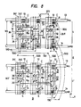
- basic cell arrays (B.C) 10 are arranged in an X direction to form a basic cell array, and the basic cell arrays are arranged in a Y direction to constitute a basic cell matrix as a whole.
- Spaces (W 1 , W' 1 ) between these B.C arrays are extension regions of external wirings, and the external wirings (1000, 1000') in the X direction and external wirings (1001, 1001', 1001") in the Y direction are extended in these regions.
- Internal wirings l IN inside the B.C array are disposed in both X and Y directions inside each B.C array in order to electrically connect each basic cell.
- the internal wiring l IN and the external wiring (1000, 1000') in the X direction consist of an aluminum first layer wiring (Al1)
- the external wiring (1001, 1001', 1001") in the Y direction consists of an aluminum second layer wiring (AQ2).
- a 2-bit decoder is constituted by use of 2-input NAND cells and inverters as shown in Fig. 10(i).
- This 2-bit decoder consists of six circuit elements G through L and in this case, one basic cells is used to constitute one circuit element.
- the utilization efficiency of the cell when the 2-input NAND cell is used will be explained with reference to Figs. 10(a) and 10(c). It is only the five basic cells (0.5 x 2 + 1 x 4) that are effectively used for the 2-bit decoder in practice.
- the cell utilization efficiency when the 3-input NAND cells are used will be explained with reference to Figs. 10(b) and 10(d).
- the utilization efficiency is 5/6 for the 2-input NAND cell whereas it is 3.3/6 for the 3- input NAND cell, and the former is higher than the latter.
- the merit and demerit of the basic cell vary depending upon the circuit (unit cell) to be fabricated.
- One of the characterizing features of the present invention lies in that the cell types to be used can be changed suitably in accordance with the circuit construction of the circuit (unit cell) to be fabricated in consideration of the merit and demerit of each cell type, and can form a desired gate array most efficiently.
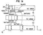
- Figs. 11(a) through 11(c) illustrate the feature of the present invention when the 3-input NAND type cells are used, wherein (a) is a logic symbol diagram, (b) is its definite layout diagram and (c) shows the channel number of external wirings extended between the cell arrays.
- Figs. 11(d) through 11(f) shows the feature of the invention when the 2-input NAND cells are used, and correspond to Figs. 11(a) through 11(c), respectively.
- Figs. 11(g) through 11(c) show the feature of the invention when modified 2-input cells in accordance with the present invention are used, and correspond to Figs. 11(a) through 11(c), respectively.
- the occupying area of one cell will be compared with reference to Figs. 11(b), (e) and (h).
- the explanation of the definite construction will be hereby omitted because it will be described elsewhere.
- the portions represented by oblique lines designate the gate of each MOSFET formed by polysilicon, and each functions as a signal input terminal.
- the lateral width of the cell increases by the width of a third signal input terminal Xa in the case of the 3-input NAND cell, and the overall lateral width amounts to l 1 + Q 2 .
- 21 external wirings are necessary therefor.
- the lateral width may be only l 1 as shown in Fig. 11(e). Since the number of the signal input terminals of each cell decreases as can be seen from Fig. 11(g), the total number of the necessary external wirings may be only 16, so that the width between the B.C array is W 1 and this is considerably smaller than W 2 in Fig. 11(c).
- the modified 2-input cell is based upon the 2-input NAND cell described above, and its occupying area as well as its wiring channel number are the same as those of the latter.
- the difference lies in that the modified 2-input cell has a built-in third signal input terminal, and the cell can be used as the 3-input NAND cell, whenever necessary, by utilizing this terminal.
- This third terminal is never connected to the external wiring but only the internal wiring l IN of the basic cell array can be connected to it.
- FIG. 12(iv) Another characterizing feature of the present invention lies in the layout of the modified 2- input cell.
- bipolar transistors as high load driving functional elements are disposed on both sides of a cell in one cell, while an MOS element is disposed at the center of the cell.
- a V cc line and a ground line (GND) extend along both edges of the cell and render no problem to the extension of the internal wiring l IN .
- the bipolar elements are disposed at the center of the cell with the MOS elements at both ends of the cell as shown in Fig. 13, the V cc line and the GND line must extend through the center of the cell so that the extension of the internal wiring l IN is prevented.
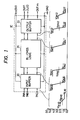
- Fig. 1 shows the overall system configuration of the gate array (IC) of the present invention and signal levels at respective portions of the gate array.
- this IC consists of an input buffer 20, a logic portion 21 consisting principally of CMOS and an output buffer 22.
- the input buffer 20 has a level converting function (and if necessary, a logic calculation function). For example, it converts input signals IN A , IN B and NN C of a TTL level received from outside to signals of a CMOS levels, and its output signal is applied to the logic portion 21 consisting principally of CMOS.
- the output buffer 22 has a level converting function of converting the signals of the CMOS level to signals of the TTL level, for example. (If necessary, a logic calculation function can be further added.) Eventually, it produces the output signals OUT 1 , OUT 2 , ..., OUT of the TTL level, for example.
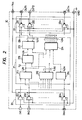
- Fig. 2 shows in further detail the internal construction of the system shown in Fig. 1.
- reference numerals 211 - 21n in the logic portion 21 represent unit cells (macrocells) and black circles or the tip portions colored in black represent that the circuit of the output stage is constituted by a bipolar circuit. (The rest of the portions are constituted by CMOSs of low power consumption type.)
- the term "unit cell (macrocell)" means a logic function block constituted by a plurality of logic elements (which are the minimum unit constituting a logic circuit and a logic function block which can not be divided any more), and represents, for example, a multiplexor or a flip-flop.
- the internal wiring of the unit cell is made by manufacturers of the IC while the wiring between the unit cells is made in accordance with a user's specification. The arrangement of each cell and the arrangement of wirings are made by use of DA (Design Automation).
- the output gate (output buffer) of each of the unit cells 211 - 21n, the input buffers 201 - 20n and the output buffers 221 - 22m is a high load driving type gate consisting of a bipolar circuit. For this reason, a signal delay quantity can be made substantially equal to a small signal delay quantity of an internal gate irrespective of the length of wirings connecting one unit to another or the magnitude of the load, and the freedom of design can be remarkably improved.
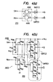
- the block 211 shown in Fig. 2 has a construction shown in Figs. 3(A) and 3(B), wherein (A) shows logic symbols and (B) does a definite circuit construction.
- the block 213 is, for example, an R-S flip-flop circuit constituted such as shown in Figs. 4(a) and 4(b).
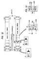
- the planar layout of the silicon chip 1 of the IC (gate array) shown in Figs. 1 and 2 will be explained with reference to Figs. 5(a) and 5(b).
- the arrays of the Bi-CMOS cells (basic cells) 10 are arranged regularly in the chip, and the input-output buffers 20, 22 are arranged around the arrays. Bonding pads are disposed around the outermost periphery.
- Fig. 5(b) is a planar layout diagram showing more definitely the layout structure of the portion A encompassed by dotted line in Fig. 5(a).
- Bonding wires 12 are connected to pads 11, and the pads and input-output buffers (20n, 22n) are connected by first layer At wirings 12.
- a power source (V ) line and a ground (GND) line consisting of a second layer Al wiring are extended on the input-output buffers (20n, 22n), and are connected to the first layer Al wiring through respective through-holes.
- V cc line 13 and the GND line 14 that are common to the input-output buffers and the basic cell arrays are extended.
- Fig. 8 shows definitely the planar layout of the region B encompassed by dotted line in Fig. 5(b), and Fig. 6(a) shows the planar layout of the basic cells (sometimes referred to as "B.C") shown in Figs. 5(a) and 5(b) with the diffusion layer in the chip being shown primarily.
- Fig. 6(b) is a sectional view taken along line X - X' in Fig. 6(a).
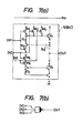
- Fig. 6(c) is a symbol diagram of the basic cell shown in Fig. 6(a).
- Fig. 7(a) shows the circuit of the basic cell and Fig. 7(b) shows the basic cell as logic symbols.
- basic cell means a basic unit of the layout construction at the logic portion formed by disposing constituent elements necessary for constituting an electronic circuit in a predetermined pattern.
- the basic cell 10 consists of the gates 30, 31, 32, n-well 50 and p-well 51 of MOSFET consisting of polysilicon, a P diffusion layer 35 as the source-drain of a P-MOSFET, an N + diffusion layer 36 as the source-drain of an N-MOSFET, diffusion layers 37, 40 (serving as emitter: E) constituting two bipolar NPN transistors Q 1 , Q 2' diffusion layers 38, 41 (as base: B), diffusion layers 39, 42 (as collector: C), and two impedance elements, that are, in this case, resistors R , R 2 .
- Fig.(6b) is a sectional view of the basic cell 10 shown in Fig. 6(a) taken along line X - X'.
- Fig. 7 shows the circuit of the basic cell 10.
- an NAND gate which is apparently of a 2-input type but is substantially of a 3-input type can be constituted by applying predetermined wirings to the elements formed inside the basic cell 10.
- Fig. 7(b) shows the basic cell 10 in the symbolized form.
- Fig. 8 shows the basic cell 10 after wiring.
- regions I, I' are those in which the basic cells 10 are arranged regularly in the X direction (horizontal to the sheet of the drawing), and will be hereinafter called the "basic cell array”.
- the wiring inside the basic cell array is made by the first layer aluminum wiring 34 in both X direction and Y direction (perpendicular to the X direction) as indicated by thick line in the drawing.
- the wiring between the basic cell arrays is made by use of the first layer aluminum wiring 51 in the X direction as shown in Fig. 1 and by use of the second layer aluminum wiring 50 (represented by dotted line in the drawing) in the Y direction.
- the region II is a wiring region in which the first layer aluminum wiring (microcell wiring) in the X direction is extended.
- the basic cell is actually a 2-input NAND gate, but it incorporates therein one more gate and hence functions substantially as a 3-input NAND gate.
- Fig. 2(a) The planar layout condition of the basic cell is shown in Fig. 2(a), and when such a modified 2-input construction is employed, the cell occupying area can be reduced for the following reasons.
- the cell area increases in the case of (b) because the gate is formed in such a manner as to extend rightward of the bipolar element (the portion represented by symbol Xa).
- the effective utilization efficiency of the cell can also be improved.
- the freedom of the wiring can be much more improved and the number of gates can be reduced by use of the 3-input NAND type cell than by use of the 2-input NAND type cell because the number of input terminals of the former is greater than that of the latter and the freedom of wiring can be improved as much.
- the wiring channel number becomes greater in the case of the 3-input NAND, and when various macrocells are constituted, the extension of the At wirings becomes a critical problem that the number of waste cells becomes greater and the chip area increases, on the contrary.
- the modified 2-input cell described above becomes substantially a 3-input NAND type cell when the second signal input terminal incorporated therein is connected by an internal wiring inside the basic cell array. Therefore, the number of gates of the circuit construction can be reduced, and since the third signal input terminal is never connected to the wiring extended in the extension region, the wiring channel number is the same as when the 2-input NAND type cell is used. As a result, the increase of the chip area due to the increase of the channel number can be prevented.
- one of the characterizing features of the present invention resides in that the reduction of the occupying area of one cell itself and the improvement in the cell utilization efficiency can be accomplished by a simple circuit construction.
- the present invention has another feature.
- the bipolar elements are disposed both outsides of MOSFET, so that the V cc line 13 and the GND line 14 are vertically extended in parallel with the basic cell array.
- two NPN transistors Q 1 and Q 2 of a totem pole connection at the output stage in the basic cell are disposed on both sides of MOSFET, and along with this arrangement, the V cc line and the GND line extend above and below the cell.
- the freedom of wiring is not at all limited by the existence of the V cc line 13 and the GND line 14.
- the V line 13 and the GND line 14 are ex- cc tended at the center of the cell 10
- the wiring in the Y direction among the internal wirings of the basic cell array (I, I' ). must step over the V cc line and the GND line, and hence a two-layered wiring must be employed. Therefore, the freedom of wiring drops and the wiring structure becomes extremely complicated.
- the gate width W of the MOSFET (M 1 ⁇ M 6 ) is reduced by several dozens of ⁇ m in comparison with that of a pure CMOS cell, and this means that the bipolar elements Q 1 , Q 2 are disposed afresh in this reduced region.
- the increase of the occupying area of the basic cell due to the disposition of the bipolar elements Q 1 , Q 2 can be minimized.
- the widths W I , W I ' of the basic cell arrays I, I' must be such that some dozens of aluminum first layer wirings 34 (e.g., 16, that is, 16 channels) in the X direction among the internal wirings of the basic cell arrays I, I' can be extended, the construction which permits to dispose the bipolar elements in the Y direction provides the advantage that sufficient W I , W I ' can be secured, and it becomes possible to cope with the increase of channels of the internal wirings of the basic array due to the miniaturization of the cell.
- the present invention can provide IC which requires less consumed power, operates at a high operating speed and has a high integration density.
- the present invention can be applied suitably to ICs which have a plurality of cells and must utilize them efficiently, particularly to gate arrays.
Landscapes
- Engineering & Computer Science (AREA)
- Power Engineering (AREA)
- Physics & Mathematics (AREA)
- Condensed Matter Physics & Semiconductors (AREA)
- General Physics & Mathematics (AREA)
- Computer Hardware Design (AREA)
- Microelectronics & Electronic Packaging (AREA)
- Design And Manufacture Of Integrated Circuits (AREA)
Applications Claiming Priority (4)
| Application Number | Priority Date | Filing Date | Title |
|---|---|---|---|
| JP60010832A JPH0815209B2 (ja) | 1985-01-25 | 1985-01-25 | 半導体集積回路装置 |
| JP10832/85 | 1985-01-25 | ||
| JP60103727A JPH0828483B2 (ja) | 1985-05-17 | 1985-05-17 | 半導体集積回路装置 |
| JP103727/85 | 1985-05-17 |
Publications (2)
| Publication Number | Publication Date |
|---|---|
| EP0189183A1 true EP0189183A1 (de) | 1986-07-30 |
| EP0189183B1 EP0189183B1 (de) | 1990-11-22 |
Family
ID=26346175
Family Applications (1)
| Application Number | Title | Priority Date | Filing Date |
|---|---|---|---|
| EP86100798A Expired - Lifetime EP0189183B1 (de) | 1985-01-25 | 1986-01-22 | Integrierte Halbleiterschaltungsanordnung |
Country Status (7)
| Country | Link |
|---|---|
| US (1) | US5001487A (de) |
| EP (1) | EP0189183B1 (de) |
| KR (1) | KR930005497B1 (de) |
| CN (1) | CN1003549B (de) |
| DE (1) | DE3675666D1 (de) |
| HK (1) | HK20893A (de) |
| SG (1) | SG102692G (de) |
Cited By (6)
| Publication number | Priority date | Publication date | Assignee | Title |
|---|---|---|---|---|
| DE3715116A1 (de) * | 1986-05-07 | 1987-11-12 | Mitsubishi Electric Corp | Integrierte halbleiterschaltung |
| EP0329152A2 (de) * | 1988-02-19 | 1989-08-23 | Kabushiki Kaisha Toshiba | Halbleiteranordnung mit Gattermatrix |
| EP0336741A2 (de) * | 1988-04-06 | 1989-10-11 | Hitachi, Ltd. | Integrierter Halbleiterschaltkreis mit Bipolartransistoren und MOSFETs |
| EP0403274A1 (de) * | 1989-06-14 | 1990-12-19 | Fujitsu Limited | Integrierte Kundenwunschschaltungsvorrichtung |
| EP0458244A2 (de) * | 1990-05-24 | 1991-11-27 | Kabushiki Kaisha Toshiba | Zell-Bibliotheks-Verfahren zur Herstellung von integrierten Halbleiterschaltungen |
| US5281835A (en) * | 1989-06-14 | 1994-01-25 | Fujitsu Limited | Semi-custom integrated circuit device |
Families Citing this family (3)
| Publication number | Priority date | Publication date | Assignee | Title |
|---|---|---|---|---|
| US5410173A (en) * | 1991-01-28 | 1995-04-25 | Kikushima; Ken'ichi | Semiconductor integrated circuit device |
| US5963057A (en) * | 1997-08-05 | 1999-10-05 | Lsi Logic Corporation | Chip level bias for buffers driving voltages greater than transistor tolerance |
| US6300800B1 (en) | 1999-11-24 | 2001-10-09 | Lsi Logic Corporation | Integrated circuit I/O buffer with series P-channel and floating well |
Citations (1)
| Publication number | Priority date | Publication date | Assignee | Title |
|---|---|---|---|---|
| EP0125504A1 (de) * | 1983-04-15 | 1984-11-21 | Hitachi, Ltd. | Hybride integrierte Halbleiterstromkreisanordnung mit bipolaren Transistoren und MOS-Transistoren |
Family Cites Families (5)
| Publication number | Priority date | Publication date | Assignee | Title |
|---|---|---|---|---|
| US4442508A (en) * | 1981-08-05 | 1984-04-10 | General Instrument Corporation | Storage cells for use in two conductor data column storage logic arrays |
| US4556947A (en) * | 1982-08-23 | 1985-12-03 | Motorola, Inc. | Bi-directional switching circuit |
| US4568961A (en) * | 1983-03-11 | 1986-02-04 | Rca Corporation | Variable geometry automated universal array |
| US4593205A (en) * | 1983-07-01 | 1986-06-03 | Motorola, Inc. | Macrocell array having an on-chip clock generator |
| US4617479B1 (en) * | 1984-05-03 | 1993-09-21 | Altera Semiconductor Corp. | Programmable logic array device using eprom technology |
-
1985
- 1985-11-23 CN CN85108621.7A patent/CN1003549B/zh not_active Expired
- 1985-12-06 KR KR1019850009158A patent/KR930005497B1/ko not_active IP Right Cessation
-
1986
- 1986-01-22 DE DE8686100798T patent/DE3675666D1/de not_active Expired - Lifetime
- 1986-01-22 EP EP86100798A patent/EP0189183B1/de not_active Expired - Lifetime
-
1990
- 1990-06-26 US US07/544,063 patent/US5001487A/en not_active Expired - Fee Related
-
1992
- 1992-10-07 SG SG1026/92A patent/SG102692G/en unknown
-
1993
- 1993-03-11 HK HK208/93A patent/HK20893A/xx not_active IP Right Cessation
Patent Citations (1)
| Publication number | Priority date | Publication date | Assignee | Title |
|---|---|---|---|---|
| EP0125504A1 (de) * | 1983-04-15 | 1984-11-21 | Hitachi, Ltd. | Hybride integrierte Halbleiterstromkreisanordnung mit bipolaren Transistoren und MOS-Transistoren |
Non-Patent Citations (1)
| Title |
|---|
| ELECTRONICS & COMMUNICATIONS IN JAPAN, vol. 66, no. 1, January 1983, pages 111-119, Scripta Publishing Co., Silver Spring, Maryland, US; M. ASANO et al.: "Design of CMOS masterslice logic LSI" * |
Cited By (12)
| Publication number | Priority date | Publication date | Assignee | Title |
|---|---|---|---|---|
| DE3715116A1 (de) * | 1986-05-07 | 1987-11-12 | Mitsubishi Electric Corp | Integrierte halbleiterschaltung |
| US4853757A (en) * | 1986-05-07 | 1989-08-01 | Mitsubishi Denki Kabushiki Kaisha | Semiconductor integrated circuit |
| EP0329152A2 (de) * | 1988-02-19 | 1989-08-23 | Kabushiki Kaisha Toshiba | Halbleiteranordnung mit Gattermatrix |
| EP0329152A3 (de) * | 1988-02-19 | 1991-01-02 | Kabushiki Kaisha Toshiba | Halbleiteranordnung mit Gattermatrix |
| EP0336741A2 (de) * | 1988-04-06 | 1989-10-11 | Hitachi, Ltd. | Integrierter Halbleiterschaltkreis mit Bipolartransistoren und MOSFETs |
| EP0336741A3 (de) * | 1988-04-06 | 1990-09-26 | Hitachi, Ltd. | Integrierter Halbleiterschaltkreis mit Bipolartransistoren und MOSFETs |
| US5220187A (en) * | 1988-04-06 | 1993-06-15 | Hitachi, Ltd. | Semiconductor integrated circuit with bipolar transistors and mosfets |
| EP0403274A1 (de) * | 1989-06-14 | 1990-12-19 | Fujitsu Limited | Integrierte Kundenwunschschaltungsvorrichtung |
| US5281835A (en) * | 1989-06-14 | 1994-01-25 | Fujitsu Limited | Semi-custom integrated circuit device |
| EP0458244A2 (de) * | 1990-05-24 | 1991-11-27 | Kabushiki Kaisha Toshiba | Zell-Bibliotheks-Verfahren zur Herstellung von integrierten Halbleiterschaltungen |
| EP0458244A3 (en) * | 1990-05-24 | 1992-01-22 | Kabushiki Kaisha Toshiba | Cell library for semiconductor integrated circuit design |
| US5387810A (en) * | 1990-05-24 | 1995-02-07 | Kabushiki Kaisha Toshiba | Cell library for semiconductor integrated circuit design |
Also Published As
| Publication number | Publication date |
|---|---|
| KR930005497B1 (ko) | 1993-06-22 |
| HK20893A (en) | 1993-03-19 |
| SG102692G (en) | 1992-12-24 |
| KR860006136A (ko) | 1986-08-18 |
| DE3675666D1 (de) | 1991-01-03 |
| CN1003549B (zh) | 1989-03-08 |
| EP0189183B1 (de) | 1990-11-22 |
| US5001487A (en) | 1991-03-19 |
| CN85108621A (zh) | 1986-07-23 |
Similar Documents
| Publication | Publication Date | Title |
|---|---|---|
| JP2912174B2 (ja) | ライブラリ群及びそれを用いた半導体集積回路 | |
| US4682202A (en) | Master slice IC device | |
| US4651190A (en) | Semiconductor integrated circuit | |
| US4827368A (en) | Semiconductor integrated circuit device | |
| JP2742052B2 (ja) | 相補型misマスタスライス論理集積回路 | |
| US5300796A (en) | Semiconductor device having an internal cell array region and a peripheral region surrounding the internal cell array for providing input/output basic cells | |
| US5378941A (en) | Bipolar transistor MOS transistor hybrid semiconductor integrated circuit device | |
| KR100223352B1 (ko) | 반도체 집적 회로 장치 | |
| US4644187A (en) | Gate array basic cell | |
| EP0189183B1 (de) | Integrierte Halbleiterschaltungsanordnung | |
| US4992845A (en) | Semiconductor integrated circuit device having input/output buffer cells each comprising a plurality of transistor regions arranged in a single line | |
| US4868630A (en) | Gate array semiconductor integrated circuit | |
| JPH0480538B2 (de) | ||
| US5404035A (en) | Multi-voltage-level master-slice integrated circuit | |
| EP0119059B1 (de) | Integrierte Halbleiterschaltung mit Gattermatrixstruktur | |
| JPH0578190B2 (de) | ||
| EP0349294B1 (de) | I/O-Zellen für integrierte Halbleiterschaltungen | |
| JPH0815209B2 (ja) | 半導体集積回路装置 | |
| JPH023279A (ja) | 相補型misマスタスライスlsiの基本セル | |
| JPS5856354A (ja) | マスタ−スライスlsi | |
| JPH0770596B2 (ja) | 半導体集積回路装置の製造方法 | |
| JPH0828483B2 (ja) | 半導体集積回路装置 | |
| JPH0566737B2 (de) | ||
| JPH0750342A (ja) | 半導体集積回路装置 | |
| JP2671537B2 (ja) | 半導体集積回路 |
Legal Events
| Date | Code | Title | Description |
|---|---|---|---|
| PUAI | Public reference made under article 153(3) epc to a published international application that has entered the european phase |
Free format text: ORIGINAL CODE: 0009012 |
|
| AK | Designated contracting states |
Kind code of ref document: A1 Designated state(s): DE FR GB IT |
|
| 17P | Request for examination filed |
Effective date: 19861219 |
|
| 17Q | First examination report despatched |
Effective date: 19881007 |
|
| GRAA | (expected) grant |
Free format text: ORIGINAL CODE: 0009210 |
|
| AK | Designated contracting states |
Kind code of ref document: B1 Designated state(s): DE FR GB IT |
|
| REF | Corresponds to: |
Ref document number: 3675666 Country of ref document: DE Date of ref document: 19910103 |
|
| ET | Fr: translation filed | ||
| ITTA | It: last paid annual fee | ||
| ITF | It: translation for a ep patent filed |
Owner name: MODIANO & ASSOCIATI S.R.L. |
|
| PLBE | No opposition filed within time limit |
Free format text: ORIGINAL CODE: 0009261 |
|
| STAA | Information on the status of an ep patent application or granted ep patent |
Free format text: STATUS: NO OPPOSITION FILED WITHIN TIME LIMIT |
|
| 26N | No opposition filed | ||
| PGFP | Annual fee paid to national office [announced via postgrant information from national office to epo] |
Ref country code: GB Payment date: 19960112 Year of fee payment: 11 |
|
| PGFP | Annual fee paid to national office [announced via postgrant information from national office to epo] |
Ref country code: FR Payment date: 19960118 Year of fee payment: 11 |
|
| PGFP | Annual fee paid to national office [announced via postgrant information from national office to epo] |
Ref country code: DE Payment date: 19960328 Year of fee payment: 11 |
|
| PG25 | Lapsed in a contracting state [announced via postgrant information from national office to epo] |
Ref country code: GB Effective date: 19970122 |
|
| GBPC | Gb: european patent ceased through non-payment of renewal fee |
Effective date: 19970122 |
|
| PG25 | Lapsed in a contracting state [announced via postgrant information from national office to epo] |
Ref country code: FR Effective date: 19970930 |
|
| PG25 | Lapsed in a contracting state [announced via postgrant information from national office to epo] |
Ref country code: DE Effective date: 19971001 |
|
| REG | Reference to a national code |
Ref country code: FR Ref legal event code: ST |
|
| PG25 | Lapsed in a contracting state [announced via postgrant information from national office to epo] |
Ref country code: IT Free format text: LAPSE BECAUSE OF NON-PAYMENT OF DUE FEES;WARNING: LAPSES OF ITALIAN PATENTS WITH EFFECTIVE DATE BEFORE 2007 MAY HAVE OCCURRED AT ANY TIME BEFORE 2007. THE CORRECT EFFECTIVE DATE MAY BE DIFFERENT FROM THE ONE RECORDED. Effective date: 20050122 |