EP0400728B1 - Integrierte Speicherschaltung mit einem Leseverstärker - Google Patents
Integrierte Speicherschaltung mit einem Leseverstärker Download PDFInfo
- Publication number
- EP0400728B1 EP0400728B1 EP90201314A EP90201314A EP0400728B1 EP 0400728 B1 EP0400728 B1 EP 0400728B1 EP 90201314 A EP90201314 A EP 90201314A EP 90201314 A EP90201314 A EP 90201314A EP 0400728 B1 EP0400728 B1 EP 0400728B1
- Authority
- EP
- European Patent Office
- Prior art keywords
- transistor
- current branch
- sense amplifier
- control transistor
- transistors
- Prior art date
- Legal status (The legal status is an assumption and is not a legal conclusion. Google has not performed a legal analysis and makes no representation as to the accuracy of the status listed.)
- Expired - Lifetime
Links
- 230000005669 field effect Effects 0.000 claims description 6
- 238000005259 measurement Methods 0.000 claims description 3
- 230000004913 activation Effects 0.000 claims description 2
- 230000008878 coupling Effects 0.000 claims description 2
- 238000010168 coupling process Methods 0.000 claims description 2
- 238000005859 coupling reaction Methods 0.000 claims description 2
- 230000007423 decrease Effects 0.000 description 4
- 230000000694 effects Effects 0.000 description 3
- 238000001514 detection method Methods 0.000 description 2
- 230000003071 parasitic effect Effects 0.000 description 2
- 238000004088 simulation Methods 0.000 description 2
- 230000003321 amplification Effects 0.000 description 1
- 238000007599 discharging Methods 0.000 description 1
- 238000000034 method Methods 0.000 description 1
- 238000003199 nucleic acid amplification method Methods 0.000 description 1
Images
Classifications
-
- G—PHYSICS
- G11—INFORMATION STORAGE
- G11C—STATIC STORES
- G11C7/00—Arrangements for writing information into, or reading information out from, a digital store
- G11C7/06—Sense amplifiers; Associated circuits, e.g. timing or triggering circuits
- G11C7/065—Differential amplifiers of latching type
-
- G—PHYSICS
- G11—INFORMATION STORAGE
- G11C—STATIC STORES
- G11C11/00—Digital stores characterised by the use of particular electric or magnetic storage elements; Storage elements therefor
- G11C11/21—Digital stores characterised by the use of particular electric or magnetic storage elements; Storage elements therefor using electric elements
- G11C11/34—Digital stores characterised by the use of particular electric or magnetic storage elements; Storage elements therefor using electric elements using semiconductor devices
- G11C11/40—Digital stores characterised by the use of particular electric or magnetic storage elements; Storage elements therefor using electric elements using semiconductor devices using transistors
- G11C11/401—Digital stores characterised by the use of particular electric or magnetic storage elements; Storage elements therefor using electric elements using semiconductor devices using transistors forming cells needing refreshing or charge regeneration, i.e. dynamic cells
- G11C11/4063—Auxiliary circuits, e.g. for addressing, decoding, driving, writing, sensing or timing
- G11C11/407—Auxiliary circuits, e.g. for addressing, decoding, driving, writing, sensing or timing for memory cells of the field-effect type
-
- G—PHYSICS
- G11—INFORMATION STORAGE
- G11C—STATIC STORES
- G11C11/00—Digital stores characterised by the use of particular electric or magnetic storage elements; Storage elements therefor
- G11C11/21—Digital stores characterised by the use of particular electric or magnetic storage elements; Storage elements therefor using electric elements
- G11C11/34—Digital stores characterised by the use of particular electric or magnetic storage elements; Storage elements therefor using electric elements using semiconductor devices
- G11C11/40—Digital stores characterised by the use of particular electric or magnetic storage elements; Storage elements therefor using electric elements using semiconductor devices using transistors
- G11C11/41—Digital stores characterised by the use of particular electric or magnetic storage elements; Storage elements therefor using electric elements using semiconductor devices using transistors forming static cells with positive feedback, i.e. cells not needing refreshing or charge regeneration, e.g. bistable multivibrator or Schmitt trigger
- G11C11/413—Auxiliary circuits, e.g. for addressing, decoding, driving, writing, sensing, timing or power reduction
- G11C11/417—Auxiliary circuits, e.g. for addressing, decoding, driving, writing, sensing, timing or power reduction for memory cells of the field-effect type
- G11C11/419—Read-write [R-W] circuits
Definitions
- the invention relates to an integrated field-effect transistor memory circuit comprising memory cells which are arranged in rows and columns, each column of memory cells being connected to a bit line and a non-bit line by way of selection means, and also comprising at least one sense amplifier which comprises a first and a second input for coupling to a bit line and an associated non-bit line of a column, each of which is coupled to a supply terminal via a load, which sense amplifier performs a current measurement on the first and the second input during the reading of information on the first and the second input, and which sense amplifier comprises a parallel connection of a first and a second current branch, each current branch comprising a control transistor having a gate, a source and a drain, the source of the control transistor in the first and the second current branch being connected to the first and the second input, respectively.
- a memory circuit of this kind is known from the article "Design tricks speed up INMOS's SRAMS” in “Electronics", April 16, 1987, p. 34.
- the cited article describes a memory circuit in which a sense amplifier senses and amplifies the information on bit lines by detection of current instead of detection of voltage differences. Consequently, the processing speed of such a sense amplifier is substantially independent of the parasitic bit line capacitance, so that a memory design may be simpler.
- an integrated field-effect transistor memory circuit in accordance with the invention is characterized in that the gate of the control transistor (T1,T2) in each current branch is connected to the drain of the control transistor (T1,T2) in the other current branch, the channel of a load transistor (T3,T4), comprising a gate, a source and a drain, being connected in between the drain of the relevant control transistor (T1,T2) and a supply terminal (Vss) in each current branch, the load transistor (T3,T4) and the control transistor (T1,T2) in each current branch having their width/length ratio (W/L) substantially equal to each other, said load transistor (T3,T4) being of the same conductivity type as the control transistor (T1, T2) in the relevant current branch, the coupled gates of said load transistors (T3,T4) receiving a selection signal for the selective activation of the sense amplifier.
- An integrated memory in accordance with the invention offers the advantage that the sense amplifier is constructed using only 4 transistors, the 4 transistors providing full equalization of the voltages on the inputs of the sense amplifier
- An embodiment of an integrated memory in accordance with the invention is characterized in that the load transistor and the control transistor in each current branch are P-type transistors. Because bit lines in a memory are usually precharged to almost the positive supply voltage in order to sustain the data integrity of the memory cell during the reading of the cell, the absolute voltage difference between the gate and the source of the control transistor should be greater than the threshold voltage of this transistor. When instead of P-type N-type control transistors are used, therefore, the gate voltage should usually be higher than the positive supply voltage, thus necessitating the use of an additional circuit for generating said gate voltage.
- Another embodiment of an integrated memory in accordance with the invention is characterized in that in each current branch a width/length ratio (W/L) of the load transistor is substantially equal to the width/length ratio (W/L) of the control transistor. Simulations performed on such a memory have demonstrated that the voltages on the gates of the control transistors are thus not latched to one of the voltages on the supply terminals. Consequently, a sense amplifier in an integrated memory in accordance with the invention is a self-restoring type, thus preventing the setting of one of the transistors from leaving the saturation region. Moreover, the implementation of such a sense amplifier on a chip is very simple.
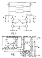
- Fig. 1 shows an embodiment of a sense amplifier in accordance with the invention.
- the sense amplifier comprises 4 PMOS-transistors T1, T2, T3 and T4.
- the sources of the transistors T1 and T2 are connected to the first input C and the second input D, respectively, of the sense amplifier.
- the junction points C and D are also connected to bit lines BL and BLN of a memory column, which bit lines BL and BLN are each connected to the supply terminal VDD via a load 1 and a load 1N, respectively.
- a number of N memory cells are connected to the bit lines BL and BLN.
- a single memory cell in a memory column can be selected, that is to say by way of row selection transistors which connect the bit line and the non-bit line to the memory cell.
- the drain of the transistors T1 and T2 is connected to the source of the transistors T3 and T4, respectively, and to junction points A and B, respectively.
- the drains of the transistors T3 and T4 are connected to data lines DL and DLN, respectively.
- the gates of the transistors T3 and T4 receive a common selection signal YSELj.
- the selection signal YSELj selects a column j, where 1 ⁇ j ⁇ m.
- the gates of the transistors T1 and T2 are connected to the drains of the transistors T2 and T1, respectively.
- the bit lines BL and BLN have a parasitic bit line capacitance CBL and CBLN, respectively, shown in parallel between respective junction points C and D and the supply terminal VSS in Fig. 1.
- the bit lines BL and BLN are first charged via the loads 1 and 1N, so that the set voltage on the junction points C and D assumes a value between the voltages on the supply terminals VSS and VDD (usually approximately 4 V in the case of a supply voltage amounting to 5 V). Consequently, the junction points A and B carry a voltage which is one threshold voltage of the transistors T1 and T2 lower than the set voltage on the junction points C and D (approximately 3 V for a threshold voltage of approximately 1 V for a set voltage of approximately 4 V). When the selection signal YSEL is subsequently logic low, the transistors T3 and T4 are turned on.
- the transistors T1, T2, T3 and T4 are proportioned so that they are all operative in the saturation region when information on the bit lines BL and BLN is read by the sense amplifier.
- the voltage differences between the gate and the source of the transistors T1 and T3, and T2 and T4, respectively are the same because of the equal currents through the transistors T1 and T3, and T2 and T4, respectively.
- the junction points A and B carry a voltage V1 and V2, respectively (selection signal YSELj is logic low).
- the gate of the respective transistor T1 and T2 thus carries a voltage V2 and V1, respectively.
- the junction points C and D thus carry a voltage (V1 + V2).
- a discharge current I depending on the information in the memory cell i.
- the junction point C is slightly discharged.
- the voltage on the junction point C slightly decreases due to the discharge current I. Because the voltages on the junction points C and D, however, are maintained equal by the sense amplifier in accordance with the invention (equalization effect), the sense amplifier also decreases the voltage on the junction point D to the same extent as the voltage decrease on the junction point C.
- a sense amplifier in accordance with the invention offers the advantage that the sensing delay of the sense amplifier is substantially independent of the bit line capacitance CBL or CBLN, because no or substantially no discharging of the bit line capacitance is required for reading the information in the memory cell i.
- junction points A and B may be connected to a further sense amplifier stage, in which case the drains of the transistors T3 and T4 can be connected to the supply terminal VSS.
- the currents through the transistors T3 and T4 can be applied to a second amplifier stage, via the data lines DL and DLN, in which a current difference can be converted into a voltage difference.
- Fig. 2 shows an embodiment of an integrated memory in accordance with the invention which comprises several sense amplifiers 4j, 4j+1 etc, whose output signals are applied to the data lines DL and DLN via mutually different currents.
- Elements in Fig. 2 which correspond to elements of Fig. 1 are denoted by corresponding references.
- the outputs of the sense amplifiers 4j, 4j+1 etc. are connected to common data lines DL and DLN.
- the sense amplifiers 4j+1 etc. are constructed in the same way as the sense amplifier 4j.
- the memory cells i in the column j and the bit line capacitances CBL and CBLN have been omitted in Fig. 2 for the sake of clarity, but are indeed present in the circuit.
- NMOS-transistors 1 consist of NMOS-transistors 1 which are connected as diodes. However, they may alternatively be formed by PMOS-transistors connected as diodes. Between each of the data lines DL and DLN and the supply terminal VSS there is included an NMOS-transistor T15, T16, respectively, connected as a diode. Furthermore, a further amplifier stage 20 is connected to the data lines DL and DLN. A buffer circuit 30 is connected to output AA of the amplifier stage 20, which buffer circuit produces an output signal on output BB.
- the operation of the circuit shown in Fig. 2 is as follows: after the selection of a single desired sense amplifier 4j in a memory column j by means of a selection signal YSELj, the information is transferred from a selected memory cell i in the relevant column j to the data lines DL and DLN by way of currents which are mutually different.
- the currents through the data lines DL and DLN are applied to the supply terminal VSS by means of the transistors T15 and T16, said currents being converted into voltages because of the diode effect of T15 and T16. Because the value of the currents through the data lines DL and DLN differs (i.e. the current I), different voltages are applied to the inputs of the further amplifier stage 20.
- the input signals are further amplified in the amplifier stage 20 and applied, via the output AA, to a buffer circuit 30.
- the buffer circuit 30 outputs an output signal having CMOS output levels on the output BB.
Landscapes
- Engineering & Computer Science (AREA)
- Microelectronics & Electronic Packaging (AREA)
- Computer Hardware Design (AREA)
- Static Random-Access Memory (AREA)
- Read Only Memory (AREA)
- Dram (AREA)
- Semiconductor Memories (AREA)
Claims (3)
- Integrierte Feldeffekttransistor-Speicherschaltung mit in Zeilen und Spalten angeordneten Speicherzellen (i...n), wobei jede Spalte aus Speicherzellen (i...n) über Selektionsmittel mit einer Bitleitung und einer Nicht-Bitleitung verbunden ist, sowie mit mindestens einem Leseverstärker, der einen ersten und einen zweiten Eingang (C, D) zum Koppeln mit einer Bitleitung und einer zugehörigen Nicht-Bitleitung einer Spalte umfaßt, von denen jeder über eine Last (1, 1N) mit einem Versorgungsanschluß (VDD) gekoppelt ist, wobei der Leseverstärker während des Lesens von am ersten und am zweiten Eingang (C, D) vorhandenen Informationen eine Strommessung am ersten und am zweiten Eingang (C, D) ausführt, und wobei der Leseverstärker eine Parallelschaltung aus einem ersten und einem zweiten Stromzweig (T1, T3; T2, T4) enthält, wobei jeder Stromzweig (T1, T3; T2, T4) einen Steuertransistor (T1, T2) mit einem Gate, einer Source und einem Drain umfaßt, wobei die Source des Steuertransistors (T1, T2) im ersten und im zweiten Stromzweig mit dem ersten bzw. zweiten Eingang (C, D) verbunden ist, dadurch gekennzeichnet, daß das Gate des Steuertransistors (T1, T2) in jedem Stromzweig mit dem Drain des Steuertransistors (T1, T2) in dem anderen Stromzweig verbunden ist, in jedem Stromzweig der Kanal eines Lasttransistors (T3, T4), welcher ein Gate, eine Source und ein Drain hat, zwischen den Drain des betreffenden Steuertransistors (T1, T2) und einen Versorgungsanschluß (Vss) geschaltet ist, wobei das Breiten/Längenverhältnis (W/L) des Lasttransistors (T3, T4) und des Steuertransistors (T1, T2) in jedem Stromzweig nahezu einander gleich sind, der genannte Lasttransistor (T3, T4) vom gleichen Leitungstyp wie der Steuertransistor (T1, T2) in dem betreffenden Stromzweig ist und die gekoppelten Gates der genannten Lasttransistoren (T3, T4) ein Selektionssignal zur selektiven Aktivierung des Leseverstärkers empfangen.
- Integrierte Feldeffekttransistor-Speicherschaltung nach Anspruch 1, dadurch gekennzeichnet, daß der Lasttransistor (T3, T4) und der Steuertransistor (T1, T2) in jedem Stromzweig p-Transistoren sind.
- Integrierte Feldeffekttransistor-Speicherschaltung nach Anspruch 1 oder 2, mit mehreren Leseverstärkern (4j, 4j+1), die an der Ausgangsseite mit dem gleichen Datenbus (DL, DLN) verbunden sind, dadurch gekennzeichnet, daß zwischen dem Datenbus (DL, DLN) und einem Versorgungsanschluß (Vss) ein als Diode geschalteter Feldeffekttransistor (T15) enthalten ist.
Applications Claiming Priority (2)
| Application Number | Priority Date | Filing Date | Title |
|---|---|---|---|
| NL8901376 | 1989-05-31 | ||
| NL8901376A NL8901376A (nl) | 1989-05-31 | 1989-05-31 | Geintegreerde geheugenschakeling met een leesversterker. |
Publications (2)
| Publication Number | Publication Date |
|---|---|
| EP0400728A1 EP0400728A1 (de) | 1990-12-05 |
| EP0400728B1 true EP0400728B1 (de) | 1995-08-02 |
Family
ID=19854753
Family Applications (1)
| Application Number | Title | Priority Date | Filing Date |
|---|---|---|---|
| EP90201314A Expired - Lifetime EP0400728B1 (de) | 1989-05-31 | 1990-05-25 | Integrierte Speicherschaltung mit einem Leseverstärker |
Country Status (11)
| Country | Link |
|---|---|
| EP (1) | EP0400728B1 (de) |
| JP (1) | JP2760634B2 (de) |
| KR (1) | KR0155374B1 (de) |
| CN (1) | CN1019614B (de) |
| CA (1) | CA2017607C (de) |
| DE (1) | DE69021273T2 (de) |
| ES (1) | ES2077630T3 (de) |
| FI (1) | FI902648A7 (de) |
| HK (1) | HK61896A (de) |
| IE (1) | IE71667B1 (de) |
| NL (1) | NL8901376A (de) |
Families Citing this family (11)
| Publication number | Priority date | Publication date | Assignee | Title |
|---|---|---|---|---|
| JP2531226Y2 (ja) * | 1992-11-26 | 1997-04-02 | 喜和 石渡 | 紙幣の収納機構 |
| DE69526336D1 (de) * | 1995-04-28 | 2002-05-16 | St Microelectronics Srl | Leseschaltung für Speicherzellen mit niedriger Versorgungsspannung |
| JPH10133908A (ja) * | 1996-10-29 | 1998-05-22 | Mitsubishi Electric Corp | マイクロプロセッサ |
| US6754119B2 (en) * | 2001-07-26 | 2004-06-22 | Samsung Electronics Co., Ltd. | Sense amplifier for memory device |
| KR100408420B1 (ko) * | 2002-01-09 | 2003-12-03 | 삼성전자주식회사 | 감지증폭기의 센싱속도를 향상시킬 수 있는 반도체메모리장치의 감지증폭기 구동회로 |
| CN1326148C (zh) * | 2002-08-14 | 2007-07-11 | 力旺电子股份有限公司 | 利用栅极互耦驱动的负载晶体管读取数据的快速存储器 |
| JP4351178B2 (ja) * | 2005-02-25 | 2009-10-28 | 寛治 大塚 | 半導体記憶装置 |
| JP2007133987A (ja) * | 2005-11-11 | 2007-05-31 | Toshiba Corp | 半導体記憶装置および半導体記憶装置の駆動方法 |
| KR100897252B1 (ko) | 2006-06-30 | 2009-05-14 | 주식회사 하이닉스반도체 | 반도체 메모리 장치 |
| CN101399018B (zh) * | 2007-09-26 | 2011-09-14 | 中华映管股份有限公司 | 信号控制电路及方法、液晶显示器及其时序控制器 |
| GB2510828B (en) * | 2013-02-13 | 2015-06-03 | Surecore Ltd | Single wordline low-power SRAM cells |
Family Cites Families (1)
| Publication number | Priority date | Publication date | Assignee | Title |
|---|---|---|---|---|
| US4039861A (en) * | 1976-02-09 | 1977-08-02 | International Business Machines Corporation | Cross-coupled charge transfer sense amplifier circuits |
-
1989
- 1989-05-31 NL NL8901376A patent/NL8901376A/nl not_active Application Discontinuation
-
1990
- 1990-05-25 ES ES90201314T patent/ES2077630T3/es not_active Expired - Lifetime
- 1990-05-25 EP EP90201314A patent/EP0400728B1/de not_active Expired - Lifetime
- 1990-05-25 DE DE69021273T patent/DE69021273T2/de not_active Expired - Lifetime
- 1990-05-28 FI FI902648A patent/FI902648A7/fi not_active Application Discontinuation
- 1990-05-28 CA CA002017607A patent/CA2017607C/en not_active Expired - Fee Related
- 1990-05-28 IE IE191090A patent/IE71667B1/en not_active IP Right Cessation
- 1990-05-28 CN CN90103239A patent/CN1019614B/zh not_active Expired
- 1990-05-30 KR KR1019900007832A patent/KR0155374B1/ko not_active Expired - Fee Related
- 1990-05-30 JP JP2138618A patent/JP2760634B2/ja not_active Expired - Lifetime
-
1996
- 1996-04-11 HK HK61896A patent/HK61896A/en not_active IP Right Cessation
Also Published As
| Publication number | Publication date |
|---|---|
| ES2077630T3 (es) | 1995-12-01 |
| EP0400728A1 (de) | 1990-12-05 |
| DE69021273T2 (de) | 1996-04-04 |
| KR0155374B1 (ko) | 1998-12-01 |
| JP2760634B2 (ja) | 1998-06-04 |
| FI902648A0 (fi) | 1990-05-28 |
| HK61896A (en) | 1996-04-19 |
| CN1019614B (zh) | 1992-12-23 |
| CN1048282A (zh) | 1991-01-02 |
| IE901910L (en) | 1990-11-30 |
| DE69021273D1 (de) | 1995-09-07 |
| IE71667B1 (en) | 1997-02-26 |
| NL8901376A (nl) | 1990-12-17 |
| CA2017607C (en) | 2001-07-24 |
| FI902648A7 (fi) | 1990-12-01 |
| JPH0319198A (ja) | 1991-01-28 |
| KR900019043A (ko) | 1990-12-22 |
| CA2017607A1 (en) | 1990-11-30 |
Similar Documents
| Publication | Publication Date | Title |
|---|---|---|
| US5689461A (en) | Semiconductor memory device having voltage booster circuit coupled to a bit line charging/equalizing circuit or switch | |
| US6466499B1 (en) | DRAM sense amplifier having pre-charged transistor body nodes | |
| US5243573A (en) | Sense amplifier for nonvolatile semiconductor storage devices | |
| US5040146A (en) | Static memory cell | |
| US4654831A (en) | High speed CMOS current sense amplifier | |
| EP0015070A1 (de) | Leseverstärkerschaltung | |
| US6304505B1 (en) | Differential correlated double sampling DRAM sense amplifier | |
| US4270190A (en) | Small signal memory system with reference signal | |
| EP0400728B1 (de) | Integrierte Speicherschaltung mit einem Leseverstärker | |
| US5253137A (en) | Integrated circuit having a sense amplifier | |
| US3946369A (en) | High speed MOS RAM employing depletion loads | |
| US6600672B2 (en) | Semiconductor memory device | |
| US4860257A (en) | Level shifter for an input/output bus in a CMOS dynamic ram | |
| JPS6035755B2 (ja) | センス増幅器 | |
| EP0374995B1 (de) | Integrierte Speicherschaltung | |
| CA1226908A (en) | Highly sensitive high performance sense amplifiers | |
| US5241504A (en) | Integrated memory comprising a sense amplifier | |
| US6205070B1 (en) | Current sense amplifier | |
| US6407580B1 (en) | Latch sense amplifier circuit with an improved next stage buffer | |
| US5525918A (en) | Pre-sense amplifier for monolithic memories | |
| US4661926A (en) | Bit line gain circuit for read only memory | |
| EP0400724B1 (de) | Integrierte Speicherschaltung mit einem Leseverstärker | |
| JPS60226092A (ja) | センスアンプ | |
| KR20030078306A (ko) | 전류차를 감지하기 위한 감지증폭기 |
Legal Events
| Date | Code | Title | Description |
|---|---|---|---|
| PUAI | Public reference made under article 153(3) epc to a published international application that has entered the european phase |
Free format text: ORIGINAL CODE: 0009012 |
|
| AK | Designated contracting states |
Kind code of ref document: A1 Designated state(s): CH DE ES FR GB IT LI SE |
|
| 17P | Request for examination filed |
Effective date: 19910530 |
|
| 17Q | First examination report despatched |
Effective date: 19931202 |
|
| GRAA | (expected) grant |
Free format text: ORIGINAL CODE: 0009210 |
|
| AK | Designated contracting states |
Kind code of ref document: B1 Designated state(s): CH DE ES FR GB IT LI SE |
|
| REF | Corresponds to: |
Ref document number: 69021273 Country of ref document: DE Date of ref document: 19950907 |
|
| ITF | It: translation for a ep patent filed | ||
| ET | Fr: translation filed | ||
| REG | Reference to a national code |
Ref country code: ES Ref legal event code: FG2A Ref document number: 2077630 Country of ref document: ES Kind code of ref document: T3 |
|
| PLBE | No opposition filed within time limit |
Free format text: ORIGINAL CODE: 0009261 |
|
| STAA | Information on the status of an ep patent application or granted ep patent |
Free format text: STATUS: NO OPPOSITION FILED WITHIN TIME LIMIT |
|
| 26N | No opposition filed | ||
| PGFP | Annual fee paid to national office [announced via postgrant information from national office to epo] |
Ref country code: CH Payment date: 19960823 Year of fee payment: 7 |
|
| PGFP | Annual fee paid to national office [announced via postgrant information from national office to epo] |
Ref country code: ES Payment date: 19970509 Year of fee payment: 8 |
|
| PGFP | Annual fee paid to national office [announced via postgrant information from national office to epo] |
Ref country code: SE Payment date: 19970527 Year of fee payment: 8 |
|
| PG25 | Lapsed in a contracting state [announced via postgrant information from national office to epo] |
Ref country code: CH Free format text: LAPSE BECAUSE OF NON-PAYMENT OF DUE FEES Effective date: 19970531 Ref country code: LI Free format text: LAPSE BECAUSE OF NON-PAYMENT OF DUE FEES Effective date: 19970531 |
|
| REG | Reference to a national code |
Ref country code: CH Ref legal event code: PL |
|
| PG25 | Lapsed in a contracting state [announced via postgrant information from national office to epo] |
Ref country code: ES Free format text: LAPSE BECAUSE OF NON-PAYMENT OF DUE FEES Effective date: 19980526 Ref country code: SE Free format text: LAPSE BECAUSE OF NON-PAYMENT OF DUE FEES Effective date: 19980526 |
|
| REG | Reference to a national code |
Ref country code: FR Ref legal event code: CD |
|
| EUG | Se: european patent has lapsed |
Ref document number: 90201314.3 |
|
| REG | Reference to a national code |
Ref country code: ES Ref legal event code: FD2A Effective date: 20000503 |
|
| REG | Reference to a national code |
Ref country code: GB Ref legal event code: IF02 |
|
| PGFP | Annual fee paid to national office [announced via postgrant information from national office to epo] |
Ref country code: FR Payment date: 20090515 Year of fee payment: 20 Ref country code: DE Payment date: 20090527 Year of fee payment: 20 Ref country code: IT Payment date: 20090520 Year of fee payment: 19 |
|
| PGFP | Annual fee paid to national office [announced via postgrant information from national office to epo] |
Ref country code: GB Payment date: 20090520 Year of fee payment: 20 |
|
| REG | Reference to a national code |
Ref country code: FR Ref legal event code: TP |
|
| PG25 | Lapsed in a contracting state [announced via postgrant information from national office to epo] |
Ref country code: GB Free format text: LAPSE BECAUSE OF EXPIRATION OF PROTECTION Effective date: 20100524 |
|
| PG25 | Lapsed in a contracting state [announced via postgrant information from national office to epo] |
Ref country code: IT Free format text: LAPSE BECAUSE OF NON-PAYMENT OF DUE FEES Effective date: 20090525 |
|
| PG25 | Lapsed in a contracting state [announced via postgrant information from national office to epo] |
Ref country code: DE Free format text: LAPSE BECAUSE OF EXPIRATION OF PROTECTION Effective date: 20100525 |