EP0378293A2 - Flüssigkristall-Anzeigevorrichtung und Verfahren zu ihrer Ansteuerung - Google Patents
Flüssigkristall-Anzeigevorrichtung und Verfahren zu ihrer Ansteuerung Download PDFInfo
- Publication number
- EP0378293A2 EP0378293A2 EP90300032A EP90300032A EP0378293A2 EP 0378293 A2 EP0378293 A2 EP 0378293A2 EP 90300032 A EP90300032 A EP 90300032A EP 90300032 A EP90300032 A EP 90300032A EP 0378293 A2 EP0378293 A2 EP 0378293A2
- Authority
- EP
- European Patent Office
- Prior art keywords
- gap
- voltage
- liquid crystal
- condition
- scanning
- Prior art date
- Legal status (The legal status is an assumption and is not a legal conclusion. Google has not performed a legal analysis and makes no representation as to the accuracy of the status listed.)
- Granted
Links
Images


Classifications
-
- G—PHYSICS
- G02—OPTICS
- G02F—OPTICAL DEVICES OR ARRANGEMENTS FOR THE CONTROL OF LIGHT BY MODIFICATION OF THE OPTICAL PROPERTIES OF THE MEDIA OF THE ELEMENTS INVOLVED THEREIN; NON-LINEAR OPTICS; FREQUENCY-CHANGING OF LIGHT; OPTICAL LOGIC ELEMENTS; OPTICAL ANALOGUE/DIGITAL CONVERTERS
- G02F1/00—Devices or arrangements for the control of the intensity, colour, phase, polarisation or direction of light arriving from an independent light source, e.g. switching, gating or modulating; Non-linear optics
- G02F1/01—Devices or arrangements for the control of the intensity, colour, phase, polarisation or direction of light arriving from an independent light source, e.g. switching, gating or modulating; Non-linear optics for the control of the intensity, phase, polarisation or colour
- G02F1/13—Devices or arrangements for the control of the intensity, colour, phase, polarisation or direction of light arriving from an independent light source, e.g. switching, gating or modulating; Non-linear optics for the control of the intensity, phase, polarisation or colour based on liquid crystals, e.g. single liquid crystal display cells
- G02F1/133—Constructional arrangements; Operation of liquid crystal cells; Circuit arrangements
-
- G—PHYSICS
- G09—EDUCATION; CRYPTOGRAPHY; DISPLAY; ADVERTISING; SEALS
- G09G—ARRANGEMENTS OR CIRCUITS FOR CONTROL OF INDICATING DEVICES USING STATIC MEANS TO PRESENT VARIABLE INFORMATION
- G09G3/00—Control arrangements or circuits, of interest only in connection with visual indicators other than cathode-ray tubes
- G09G3/20—Control arrangements or circuits, of interest only in connection with visual indicators other than cathode-ray tubes for presentation of an assembly of a number of characters, e.g. a page, by composing the assembly by combination of individual elements arranged in a matrix no fixed position being assigned to or needed to be assigned to the individual characters or partial characters
- G09G3/34—Control arrangements or circuits, of interest only in connection with visual indicators other than cathode-ray tubes for presentation of an assembly of a number of characters, e.g. a page, by composing the assembly by combination of individual elements arranged in a matrix no fixed position being assigned to or needed to be assigned to the individual characters or partial characters by control of light from an independent source
- G09G3/36—Control arrangements or circuits, of interest only in connection with visual indicators other than cathode-ray tubes for presentation of an assembly of a number of characters, e.g. a page, by composing the assembly by combination of individual elements arranged in a matrix no fixed position being assigned to or needed to be assigned to the individual characters or partial characters by control of light from an independent source using liquid crystals
- G09G3/3611—Control of matrices with row and column drivers
- G09G3/3674—Details of drivers for scan electrodes
- G09G3/3681—Details of drivers for scan electrodes suitable for passive matrices only
-
- G—PHYSICS
- G02—OPTICS
- G02F—OPTICAL DEVICES OR ARRANGEMENTS FOR THE CONTROL OF LIGHT BY MODIFICATION OF THE OPTICAL PROPERTIES OF THE MEDIA OF THE ELEMENTS INVOLVED THEREIN; NON-LINEAR OPTICS; FREQUENCY-CHANGING OF LIGHT; OPTICAL LOGIC ELEMENTS; OPTICAL ANALOGUE/DIGITAL CONVERTERS
- G02F1/00—Devices or arrangements for the control of the intensity, colour, phase, polarisation or direction of light arriving from an independent light source, e.g. switching, gating or modulating; Non-linear optics
- G02F1/01—Devices or arrangements for the control of the intensity, colour, phase, polarisation or direction of light arriving from an independent light source, e.g. switching, gating or modulating; Non-linear optics for the control of the intensity, phase, polarisation or colour
- G02F1/13—Devices or arrangements for the control of the intensity, colour, phase, polarisation or direction of light arriving from an independent light source, e.g. switching, gating or modulating; Non-linear optics for the control of the intensity, phase, polarisation or colour based on liquid crystals, e.g. single liquid crystal display cells
- G02F1/137—Devices or arrangements for the control of the intensity, colour, phase, polarisation or direction of light arriving from an independent light source, e.g. switching, gating or modulating; Non-linear optics for the control of the intensity, phase, polarisation or colour based on liquid crystals, e.g. single liquid crystal display cells characterised by the electro-optical or magneto-optical effect, e.g. field-induced phase transition, orientation effect, guest-host interaction or dynamic scattering
- G02F1/139—Devices or arrangements for the control of the intensity, colour, phase, polarisation or direction of light arriving from an independent light source, e.g. switching, gating or modulating; Non-linear optics for the control of the intensity, phase, polarisation or colour based on liquid crystals, e.g. single liquid crystal display cells characterised by the electro-optical or magneto-optical effect, e.g. field-induced phase transition, orientation effect, guest-host interaction or dynamic scattering based on orientation effects in which the liquid crystal remains transparent
- G02F1/141—Devices or arrangements for the control of the intensity, colour, phase, polarisation or direction of light arriving from an independent light source, e.g. switching, gating or modulating; Non-linear optics for the control of the intensity, phase, polarisation or colour based on liquid crystals, e.g. single liquid crystal display cells characterised by the electro-optical or magneto-optical effect, e.g. field-induced phase transition, orientation effect, guest-host interaction or dynamic scattering based on orientation effects in which the liquid crystal remains transparent using ferroelectric liquid crystals
-
- G—PHYSICS
- G09—EDUCATION; CRYPTOGRAPHY; DISPLAY; ADVERTISING; SEALS
- G09G—ARRANGEMENTS OR CIRCUITS FOR CONTROL OF INDICATING DEVICES USING STATIC MEANS TO PRESENT VARIABLE INFORMATION
- G09G3/00—Control arrangements or circuits, of interest only in connection with visual indicators other than cathode-ray tubes
- G09G3/20—Control arrangements or circuits, of interest only in connection with visual indicators other than cathode-ray tubes for presentation of an assembly of a number of characters, e.g. a page, by composing the assembly by combination of individual elements arranged in a matrix no fixed position being assigned to or needed to be assigned to the individual characters or partial characters
- G09G3/34—Control arrangements or circuits, of interest only in connection with visual indicators other than cathode-ray tubes for presentation of an assembly of a number of characters, e.g. a page, by composing the assembly by combination of individual elements arranged in a matrix no fixed position being assigned to or needed to be assigned to the individual characters or partial characters by control of light from an independent source
- G09G3/36—Control arrangements or circuits, of interest only in connection with visual indicators other than cathode-ray tubes for presentation of an assembly of a number of characters, e.g. a page, by composing the assembly by combination of individual elements arranged in a matrix no fixed position being assigned to or needed to be assigned to the individual characters or partial characters by control of light from an independent source using liquid crystals
- G09G3/3611—Control of matrices with row and column drivers
- G09G3/3622—Control of matrices with row and column drivers using a passive matrix
- G09G3/3629—Control of matrices with row and column drivers using a passive matrix using liquid crystals having memory effects, e.g. ferroelectric liquid crystals
-
- G—PHYSICS
- G09—EDUCATION; CRYPTOGRAPHY; DISPLAY; ADVERTISING; SEALS
- G09G—ARRANGEMENTS OR CIRCUITS FOR CONTROL OF INDICATING DEVICES USING STATIC MEANS TO PRESENT VARIABLE INFORMATION
- G09G3/00—Control arrangements or circuits, of interest only in connection with visual indicators other than cathode-ray tubes
- G09G3/20—Control arrangements or circuits, of interest only in connection with visual indicators other than cathode-ray tubes for presentation of an assembly of a number of characters, e.g. a page, by composing the assembly by combination of individual elements arranged in a matrix no fixed position being assigned to or needed to be assigned to the individual characters or partial characters
- G09G3/34—Control arrangements or circuits, of interest only in connection with visual indicators other than cathode-ray tubes for presentation of an assembly of a number of characters, e.g. a page, by composing the assembly by combination of individual elements arranged in a matrix no fixed position being assigned to or needed to be assigned to the individual characters or partial characters by control of light from an independent source
- G09G3/36—Control arrangements or circuits, of interest only in connection with visual indicators other than cathode-ray tubes for presentation of an assembly of a number of characters, e.g. a page, by composing the assembly by combination of individual elements arranged in a matrix no fixed position being assigned to or needed to be assigned to the individual characters or partial characters by control of light from an independent source using liquid crystals
- G09G3/3611—Control of matrices with row and column drivers
- G09G3/3685—Details of drivers for data electrodes
- G09G3/3692—Details of drivers for data electrodes suitable for passive matrices only
-
- G—PHYSICS
- G02—OPTICS
- G02F—OPTICAL DEVICES OR ARRANGEMENTS FOR THE CONTROL OF LIGHT BY MODIFICATION OF THE OPTICAL PROPERTIES OF THE MEDIA OF THE ELEMENTS INVOLVED THEREIN; NON-LINEAR OPTICS; FREQUENCY-CHANGING OF LIGHT; OPTICAL LOGIC ELEMENTS; OPTICAL ANALOGUE/DIGITAL CONVERTERS
- G02F1/00—Devices or arrangements for the control of the intensity, colour, phase, polarisation or direction of light arriving from an independent light source, e.g. switching, gating or modulating; Non-linear optics
- G02F1/01—Devices or arrangements for the control of the intensity, colour, phase, polarisation or direction of light arriving from an independent light source, e.g. switching, gating or modulating; Non-linear optics for the control of the intensity, phase, polarisation or colour
- G02F1/13—Devices or arrangements for the control of the intensity, colour, phase, polarisation or direction of light arriving from an independent light source, e.g. switching, gating or modulating; Non-linear optics for the control of the intensity, phase, polarisation or colour based on liquid crystals, e.g. single liquid crystal display cells
- G02F1/133—Constructional arrangements; Operation of liquid crystal cells; Circuit arrangements
- G02F1/1333—Constructional arrangements; Manufacturing methods
- G02F1/1335—Structural association of cells with optical devices, e.g. polarisers or reflectors
- G02F1/133509—Filters, e.g. light shielding masks
- G02F1/133512—Light shielding layers, e.g. black matrix
-
- G—PHYSICS
- G09—EDUCATION; CRYPTOGRAPHY; DISPLAY; ADVERTISING; SEALS
- G09G—ARRANGEMENTS OR CIRCUITS FOR CONTROL OF INDICATING DEVICES USING STATIC MEANS TO PRESENT VARIABLE INFORMATION
- G09G2310/00—Command of the display device
- G09G2310/02—Addressing, scanning or driving the display screen or processing steps related thereto
- G09G2310/0202—Addressing of scan or signal lines
- G09G2310/0205—Simultaneous scanning of several lines in flat panels
-
- G—PHYSICS
- G09—EDUCATION; CRYPTOGRAPHY; DISPLAY; ADVERTISING; SEALS
- G09G—ARRANGEMENTS OR CIRCUITS FOR CONTROL OF INDICATING DEVICES USING STATIC MEANS TO PRESENT VARIABLE INFORMATION
- G09G2310/00—Command of the display device
- G09G2310/06—Details of flat display driving waveforms
-
- G—PHYSICS
- G09—EDUCATION; CRYPTOGRAPHY; DISPLAY; ADVERTISING; SEALS
- G09G—ARRANGEMENTS OR CIRCUITS FOR CONTROL OF INDICATING DEVICES USING STATIC MEANS TO PRESENT VARIABLE INFORMATION
- G09G2310/00—Command of the display device
- G09G2310/06—Details of flat display driving waveforms
- G09G2310/061—Details of flat display driving waveforms for resetting or blanking
-
- G—PHYSICS
- G09—EDUCATION; CRYPTOGRAPHY; DISPLAY; ADVERTISING; SEALS
- G09G—ARRANGEMENTS OR CIRCUITS FOR CONTROL OF INDICATING DEVICES USING STATIC MEANS TO PRESENT VARIABLE INFORMATION
- G09G2320/00—Control of display operating conditions
- G09G2320/02—Improving the quality of display appearance
- G09G2320/0209—Crosstalk reduction, i.e. to reduce direct or indirect influences of signals directed to a certain pixel of the displayed image on other pixels of said image, inclusive of influences affecting pixels in different frames or fields or sub-images which constitute a same image, e.g. left and right images of a stereoscopic display
-
- G—PHYSICS
- G09—EDUCATION; CRYPTOGRAPHY; DISPLAY; ADVERTISING; SEALS
- G09G—ARRANGEMENTS OR CIRCUITS FOR CONTROL OF INDICATING DEVICES USING STATIC MEANS TO PRESENT VARIABLE INFORMATION
- G09G3/00—Control arrangements or circuits, of interest only in connection with visual indicators other than cathode-ray tubes
- G09G3/20—Control arrangements or circuits, of interest only in connection with visual indicators other than cathode-ray tubes for presentation of an assembly of a number of characters, e.g. a page, by composing the assembly by combination of individual elements arranged in a matrix no fixed position being assigned to or needed to be assigned to the individual characters or partial characters
- G09G3/2007—Display of intermediate tones
Definitions
- the present invention relates to a liquid crystal display device having a ferroelectric liquid crystal layer, particularly to an liquid crystal display device having a fine pattern of fine pixel pitches and narrow gaps between pixels and its driving method.
- Ferroelectric liquid crystal has been attracted attention as a new liquid crystal device which has spontaneous polarisation with a response time of a microsecond order with a memory feature in a thin layer cell.
- the configuration of the conventional ferroelectric liquid crystal element is that a ferroelectric liquid crystal is sandwiched between two substrates each having a pattern of stripe-shaped transparent electrodes formed on a glass and two an alignment layer formed on the electrode pattern.
- the substrates are disposed such that the electrode pat terns are in a perpendicular relation to each other.
- the alignment layer is a high polymer having been rubbed or an obliquely deposited inorganic material layer such as SiO.
- the Chiral Smectic C phase as a typical ferroelectric liquid crystal has a layer structure.
- the molecules take a spiral structure in a normal line direction to the layer.
- the spiral is loosened and thus several conditions become stable in which the molecules are uniformly directed in one direction due to the interaction with a substrate surface. An electric field allows switching between these conditions, and as this switch shows an abrupt threshold, the matrix drive is feasible.
- the twist state is induced by an intermediate voltage of the voltage necessary to switch between the two uniform states, and it becomes a gray indication in the about arrangement of the polarizers.
- the stability of these stable conditions depends on the polarities of the upper and lower substrates, and the initial molecular orientations immediately after the ferroelectric liquid crystal was sandwiched in a symmetrically structured cell contain two uniform states in a mixed mode or take a twist state. So far the liquid crystal condition outside the pixel has been considered that it is kept as the initial molecular orientation and is not responsive to the electrical field.
- a light shielding layer is essential in order to obtain an indication of better contrast because an opening ratio (a ratio of the pixel area to the whole display area) becomes smaller.
- an opening ratio a ratio of the pixel area to the whole display area
- the pixel pattern becomes smaller, it becomes difficult to form a light shielding layer precisely between the pixels and the cost thereof becomes higher.
- the opening ratio becomes smaller to result in image a dark indication.
- an object of the present invention is to provide a ferroelectric liquid crystal display device and its driving method that allow a high contrast and bright display with a simple configuration and yet a uniform gray scale without increasing the number of electrodes.
- the present invention provides a liquid crystal display device comprising a liquid crystal panel in which a ferroelectric liquid crystal is sandwiched between opposing substrates each having formed thereon a plurality of electrodes of form a plurality of pixels , and a means for applying predetermined voltages to adjacent pixels for switching a stable state of a gap between the adjacent pixels.
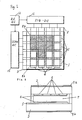
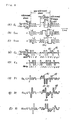
- Fig. 1 is a plan view of a liquid crystal display device of the present invention and is comprised by a liquid crystal panel 1 and driving circuits 10 - 12.
- a ferroelectric liquid crystal is sandwiched between an upper substrate 2 having signal electrodes 4 and a lower substrate 3 having scanning electrodes 5.
- Pixel pitch is 90 ⁇ m while gap between pixels is 5 ⁇ m.
- Fig. 2 shows a section views of liquid crystal panel 1, in which each pattern of stripe-shaped transparent electrodes 4 and 5 is formed on a grass and an alignment layer 6 is formed on each electrode pattern.
- the liquid crystal may be an ester ferroelectric liquid crystal.
- the thickness of liquid crystal layer 7 is 2.0 ⁇ m.
- Alignment layer layer 6 is formed by depositing SiO in a direction inclined by 82° from the substrate normal line.
- the bright and shade pattern is displayed with a birefringence effect by pasting polarizers 9a and 9b in a right angle to each other on the upper and lower substrates.
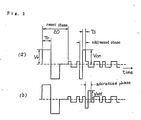
- a driving circuit part is composed of a scanning electrode driving circuit (SCAN-DC) 10, a signal electrode driving circuit 11 (SIG-DC), and a base signal generating circuit 12 (BSGC) . With these circuits, the driving waveform as shown in Fig. 3 is applied to each pixel of liquid crystal panel 1. The display state after the driving waveform is applied to each pixei is shown in Fig.
- Fig. 3 shows a voltage to be applied to an ON pixel connected to a certain scanning electrode, and Fig. 3 (b) a voltage to an OFF pixel connected to the following scanning electrode. Scanning by a voltage selection scheme is carried out after making the whole panel dark condition at reset phase 20.
- the voltage and pulse width at which a stable condition of the gap is changed becomes smaller.
- the ON pixel in area 8b in Fig. 1 becomes a bright condition and the liquid crystal at the gap between the ON pixels takes a twisted condition to be a medium level.
- the area 8a remains in the same condition as Fig. 1.
- the threshold value at the pixel area in the third panel is a little raised at 25 volts and 225 ⁇ sec and a difference from that at the gap becomes very small.
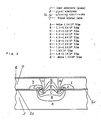
- Fig. 4 shows a section view of a liquid crystal shown with a distribution of electric field strength calculated with a finite element method to know what electric field is applied to the liquid crystal layer around the gap between pixels when applying a voltage to the whole panel .
- Calculation was made in such a manner that voltage of signal electrode 4 (hatching area) is 0 volt, voltage of scanning electrode 5 l and 5 r (hatching area) is 20 volt, thickness of liquid crystal layer 2 ⁇ m, thickness of electrode 4, 5 l , and 5r, is of 200 nm, dielectric constants of liquid crystal layer 7 and lower substrate (glass) 3 are 7 and 6.7 respectively, the gap between scanning electrode 5 l and 5 r is 4 um.
- the inside of the panel was divided into areas A to K. The electric field strengths at the respective areas are shown in the figure.
- the area A corresponds to the weakest electric field strength while the area K corresponds to the strongest electric field strength.
- the cell with less than 30um of the gap can be made a black matrix condition in the driving wave form in Fig. 3 by increasing the voltage or widening the pulse width.
- ferroelectric liquid crystal material having large amount of ionic impurity with 1010 ⁇ /cm or less of volume resistivity in the liquid crystal layer even if the pulse width is lengthened, it could not make the gap completely dark in case the gap between pixels is 5 ⁇ m or more. This is so considered that the ionic impurities move due to the applied voltage, and then a voltage reverse to the applied voltage is generated because of ion distribution.
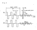
- a method to insert a reset phase when another scanning line is selected as shown in Fig. 6 allows a continuous scanning to be made.
- (a), (b) and (c) are voltages to be applied to scanning electrodes S i , S i+1 and S i+2
- (d) and (e) are voltages to be applied to any signal electrodes C1 and C2
- (f) and (h) are voltages to be applied to pixels P1(Si, C1), P2(S i+1 , C1) and P3(S i+2 , C1).
- the applied voltages of the non-addressed phase other than the addressed phase and reset phase are the same as those of the voltage selection scheme.
- pulse 45 at voltage ⁇ V0/2 in addressed phase is applied, to the signal electrode pulse 46 at voltage ⁇ V0/2 in case data being 1, and in case data being 0 pulse 47 at voltage ⁇ (1/2 - 2/a)V0 is applied.
- 1/a is a bias ratio which is an appropriate real number from 3 to 6 set in accordance with the threshold of the liquid crystal.
- AC pulse of voltage V0/a is applied to a pixel by applying the voltage of ⁇ (1/2 - 1/a)V0 to a scanning electrode.
- AC pulse 40a at voltage ⁇ V0/2 with wide pulse width which is reverse to pulse 45 in polarity of the addressed phase, is applied to the scanning electrode prior to addressed phase 38.
- a certain reset phase of a scanning line is overlapped with an addressed phase of other scanning lines.
- reset phase 39 in Fig. 6 S i+2 is overlapped with addressed phase 38 of S i . Therefore, in reset phase 39 of S i+2 data of pixels on the scanning line other than S i+2 is inputted to signal electrodes C1 and C2.
- the reset pulses to be applied to the pixels do not also contain DC (direct curre nt) components.
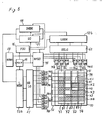
- Fig. 7 Detailed block diagrams for driving circuits 10, 11 and 12 in Fig. 1 are shown in Fig. 7. These circuits allow the driving waveforms in Fig. 3, Fig. 5 and Fig. 6 to be implemented.
- BCGC base clock generating circuit
- FDIV frequency-divider
- Scanning circuit (SC) 50 and selection circuit (SELC) 51 sends a selection pulse, which selects in turn a scanning electrode, to scanning line driver circuits (SCANLDC) 52 - 57 by receiving the clock pulse from FDIV 59.
- SCANLDC 52 - 57 select a scanning voltage generated in BPGC60 in accordance with the selection pulse.
- signal line drive circuits (SIGLDC) 63 - 68 selects a signal voltage from BPGC 60 in accordance with selection pulses Vc1 and Vc2 generated by selection circuit 62 according to data sent from display memory (DMEM) 61.
- the liquid crystal display device of the present invention implements a light valve with high contrast ratio and high transmittance (reflectance in case of reflection type) by means of a simple configuration without light shielding layer in the gap between pixels, even if the pattern is very fine and the opening ratio cannot be large enough.
- an alignment layer is formed by means of oblique evaporation in the present embodiment, even an alignment layer rubbed with organic polymer and an organic polymer thin layer formed by means of Langmuir-blodgett method can give the same effect.
- an opening ratio of 100% can be displayed by switching stable conditions of both gap and pixel, even if the width of the gap is 5 ⁇ m.
- the liquid crystal display device of the present invention is effective as a photomask to be used for making semiconductor integrated circuits, etc.
- merely sending out data to a liquid crystal drive circuit serves as photomasking instead of making fixed pattern by etching shielding layer like chrome and the like.
- a pixel pitch of the liquid crystal display device of the present invention is a pattern of at most several 10 ⁇ m
- a display device having a large, high precision/high capacity, bright, and high contrast is structured by projecting the pattern onto a screen on a large scale.
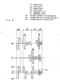
- Fig. 8 shows a block diagram of a driving circuit and a plan view of a liquid crystal display device equipped with a driving circuit and a ferroelectric liquid crystal matrix panel 70 in which a pixel pitch is 24 ⁇ m, and each vertical gap consisting of y1 to y3 is 4 ⁇ m located between column electrodes Y1 to Y4 on the upper substrate 71, and each horizontal gap consisting of x1 to x3 is 8 ⁇ m located between row electrodes X1 to X4 on the lower substrate 72.
- Liquid crystal panel 70 forms a transparent electrode of a stripe shape on the grass in the same manner as shown in Fig. 2 of the embodiment 1, and an alignment layer is formed thereon and has no light shielding layer on the gap.
- the liquid crystal material, thickness of the liquid crystal layer, and a forming method for alignment layer are the same as those of embodiment 1.
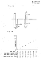
- Fig. 10 and 11 are characteristic diagrams measured for a light transmittance to a pulse width of applied voltage, and a light transmittance to a applied voltage in liquid crystal panel 70 in Fig. 8.
- the method of measurement is made by measuring a light transmittance when the memory condition of the pixels are stabled, after the voltage is applied to all of the pixels as shown in Fig. 12.
- the voltage wave form in Fig. 12 is formed by applying bipolar test pulse 91 at pulse width ⁇ and voltage Vt, after making the whole panel completely dark with reset pulse 90 at 25 volts and pulse width 1 millisecond.
- bipolar test pulse 91 at pulse width ⁇ and voltage Vt
- a, b and c show respectively characteristic curves measured of pixel (X1, Y1), gap between pixels (X1, Y3) and (x1, Y3) in the unit pixel as enclosed by a dotted line when pulse width of pulse 91 is changed while the voltage is fixed.
- a, b and c there are respective transmittance rises with switchover in stability at 200 microsec, 500 microsec, and 800 microsec, respectively.
- 11 a1 , b1, and c1 show a transmittance characteristic curve to the voltage applied to pixel (X1, Y3), gap (X1, y3) and (x1, Y3) when ⁇ is fixed at 500 microsec, and respective threshold voltages 0 to about 8 volts, 22 volts, and 32 volts.
- these gaps between pixels likewise showed bistability like the pixel inside, and it has become clear that the wider the gap, the bigger the threshold voltage.
- even a pulse of 25 volt at 1 millisecond does not allow the stability of the gap between pixels to be switched.
- gray scale display is made by combining brightness inside the pixel and the gap between pixels by applying the driving waveform as shown in Fig. 9 to the liquid crystal panel.
- the driving waveform in Fig. 9 first of all making the whole panel black by applying reset pulses in reset phase 80 of 1 millisecond at ⁇ 25 volts to entire pixels, bright and dark are written to the pixel and two kinds of gaps in turn from a portion having a longer threshold pulse width with 3 times scanning from 81 to 83.
- 86 is a voltage to be applied to row electrode X1 in Fig.
- 87 is a voltage to be applied to column electrode Y3, 88 is a voltage to be applied to pixel (X1, Y3) .
- first scanning 81 two adjacent row electrodes X1 and X2, at pulse width 800 microsecond are selected simultaneously.
- the bipolar pulse during addressed phase 84 is set at a reverse polarity to reset pulses in reset phase 80, and an ON voltage sufficient to reverse the brightness in the gap at data being 1 is given to the pixels while at an data being 0 an OFF voltage on which darkness is kept is applied to pixels.
- the horizontal axis represents input gray scale data of the second field 82, the first field 81, and the third field 83 in turn from an upper position inside the bracket.
- the axis of ordinates represents the transmittance of a unit pixel 79, but each gray scale is of almost the same equal interval as the ratio of an area in which bright and darkness are written in each of the first, second and third field is made to be nearly 4 to 2 to 1.
- a flag output to show the scanning direction in accordance with the field number is outputted by counting the field number by field counting circuit (FCC) 76.
- FCC field counting circuit
- base pulse voltage generating circuit BPGC 75 switches an output direction of the scanning voltage and the signal voltage.
- the output signal of scanning circuit (SC) 77 and display memory 78 also switches an output direction in accordance with the flag signal of FCC 76. Namely, when scanning the row electrodes, the output of SC77 is outputted to line memory (LMEM) 73a and the output of DMEM78 is to line memory (LMEM) 73b.
- selection circuits (SELC) 51 and 62 send selection pulses to signal line driving circuits (SIGLDC) 74 a - 74 l.
- SIGLDC 74 a - 74 l select the voltage of BPGC 75 in accordance with the selection pulse.
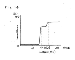
- Fig. 14 represents a characteristic diagram of a light transmittance to an applied voltage of the ferroelectric liquid crystal panel by taking the gap between pixels of the signal electrode at pixel pitch l8 ⁇ m to be 2 ⁇ m and the gap between pixels of the scanning electrode to be 4 ⁇ m. Measurement was made with a wave form shown in Fig. 11 at a pulse width of 250 ⁇ s.
- the axis of abscissa represents voltage Vt of test pulse 91 while the axis of ordinate represents transmittance in case transmitted lights of both the pixel and the gap between pixels are added.
- the transmittance has increased to about 70 % because only the pixel inverted from a dark condition to a bright condition at 17 volt. Then, the gap between pixels on the signal electrode inverted at about 23 volt, and the transmittance increased stepwise to about 80 %. Therefore, in the driving waveforms as shown in Fig. 3, Fig. 5 and Fig.
- the driving circuit has the same configuration as the one in Fig. 7, and the aforementioned intermediate voltage is supplied from BPGC to the 3rd SIGLDC by increasing SIGLDC to 3 pieces per 1 electrode that are horizontally aligned.
- the liquid crystal display device of the present invention allows multi-gray scale display to be implemented with the same number of electrodes with the conventional ferroelectric liquid crystal display device by controlling the condition of the gap between pixels in case the pattern is very fine, with the application of voltage through pixel electrodes.
Landscapes
- Physics & Mathematics (AREA)
- Engineering & Computer Science (AREA)
- Chemical & Material Sciences (AREA)
- Crystallography & Structural Chemistry (AREA)
- General Physics & Mathematics (AREA)
- Nonlinear Science (AREA)
- Computer Hardware Design (AREA)
- Theoretical Computer Science (AREA)
- Optics & Photonics (AREA)
- Mathematical Physics (AREA)
- Liquid Crystal Display Device Control (AREA)
- Liquid Crystal (AREA)
Applications Claiming Priority (4)
| Application Number | Priority Date | Filing Date | Title |
|---|---|---|---|
| JP2422/89 | 1989-01-09 | ||
| JP1002422A JPH0812347B2 (ja) | 1989-01-09 | 1989-01-09 | 液晶素子とその駆動法 |
| JP1133442A JPH087343B2 (ja) | 1989-05-26 | 1989-05-26 | 液晶素子とその駆動法 |
| JP133442/89 | 1989-05-26 |
Publications (3)
| Publication Number | Publication Date |
|---|---|
| EP0378293A2 true EP0378293A2 (de) | 1990-07-18 |
| EP0378293A3 EP0378293A3 (de) | 1991-06-26 |
| EP0378293B1 EP0378293B1 (de) | 1994-09-14 |
Family
ID=26335779
Family Applications (1)
| Application Number | Title | Priority Date | Filing Date |
|---|---|---|---|
| EP90300032A Expired - Lifetime EP0378293B1 (de) | 1989-01-09 | 1990-01-03 | Flüssigkristall-Anzeigevorrichtung und Verfahren zu ihrer Ansteuerung |
Country Status (4)
| Country | Link |
|---|---|
| US (1) | US5151803A (de) |
| EP (1) | EP0378293B1 (de) |
| KR (1) | KR940006990B1 (de) |
| DE (1) | DE69012353T2 (de) |
Cited By (8)
| Publication number | Priority date | Publication date | Assignee | Title |
|---|---|---|---|---|
| GB2266985A (en) * | 1992-05-15 | 1993-11-17 | Marconi Gec Ltd | Ferroelectric liquid crystal displays |
| EP0762377A3 (de) * | 1995-08-18 | 1997-12-03 | Sony Corporation | Ansteuerungsverfahren für eine Flüssigkristallvorrichtung |
| EP0811866A4 (de) * | 1995-12-14 | 1998-12-02 | Seiko Epson Corp | Verfahren zum betrieb einer anzeige, anzeige und elektronische vorrichtung |
| US5963186A (en) * | 1990-08-07 | 1999-10-05 | The Secretary Of State For Defence In Her Britannic Majesty's Government Of The United Kingdom Of Great Britain And Northern Ireland | Multiplex addressing of ferro-electric liquid crystal displays |
| US6243063B1 (en) | 1997-06-12 | 2001-06-05 | Sharp Kabushiki Kaisha | Diffractive spatial light modulator and display |
| EP1630779A2 (de) | 2004-08-27 | 2006-03-01 | Idc, Llc | Angeizevorrichtung mit mikroelektromechanischen Systemen (MEMS) und Verfahren zur Steuerung einer solchen Vorrichtung |
| US7545554B2 (en) | 2003-12-09 | 2009-06-09 | Idc, Llc | MEMS display |
| CN100585674C (zh) * | 2004-08-27 | 2010-01-27 | Idc公司 | 用于寻址mems显示器的系统和方法 |
Families Citing this family (25)
| Publication number | Priority date | Publication date | Assignee | Title |
|---|---|---|---|---|
| JP2915104B2 (ja) * | 1990-07-30 | 1999-07-05 | キヤノン株式会社 | 液晶素子および液晶駆動方法 |
| US5815133A (en) * | 1992-11-17 | 1998-09-29 | Canon Kabushiki Kaisha | Display apparatus |
| EP0605865B1 (de) * | 1992-12-28 | 1998-03-25 | Canon Kabushiki Kaisha | Verfahren und Einrichtung für eine Flüssigkristallanzeige |
| US6011528A (en) * | 1993-11-28 | 2000-01-04 | Smartlight Ltd. | Display device |
| JPH07152017A (ja) | 1993-11-30 | 1995-06-16 | Sony Corp | 液晶素子の駆動方法及びその液晶素子 |
| JPH07261149A (ja) * | 1994-03-23 | 1995-10-13 | Seiko Instr Inc | 液晶装置 |
| US5610739A (en) * | 1994-05-31 | 1997-03-11 | Matsushita Electric Industrial Co., Ltd. | Liquid crystal display unit with a plurality of subpixels |
| US5748164A (en) * | 1994-12-22 | 1998-05-05 | Displaytech, Inc. | Active matrix liquid crystal image generator |
| JPH08202294A (ja) * | 1995-01-20 | 1996-08-09 | Dainippon Printing Co Ltd | 液晶表示媒体の液晶配向方法及び液晶配向装置 |
| JP3406772B2 (ja) * | 1996-03-28 | 2003-05-12 | 株式会社東芝 | アクティブマトリクス型液晶表示装置 |
| JPH09281508A (ja) * | 1996-04-12 | 1997-10-31 | Semiconductor Energy Lab Co Ltd | 液晶表示装置およびその作製方法 |
| JP3392672B2 (ja) * | 1996-11-29 | 2003-03-31 | 三洋電機株式会社 | 表示装置 |
| CN1314997A (zh) * | 1998-06-16 | 2001-09-26 | 奥宝科技有限公司 | 检查基本平坦平面的发光器 |
| CN1287626A (zh) * | 1998-10-22 | 2001-03-14 | 西铁城时计株式会社 | 铁电液晶显示器件及其驱动方法 |
| JP2002055657A (ja) | 2000-08-08 | 2002-02-20 | Sharp Corp | 映像表示装置 |
| US6767609B2 (en) * | 2000-09-15 | 2004-07-27 | 3M Innovative Properties Company | Perforated film constructions for backlit signs |
| US7136036B2 (en) | 2000-11-30 | 2006-11-14 | Thomson Licensing | Method and apparatus for uniform brightness in displays |
| JP2002311449A (ja) * | 2001-02-06 | 2002-10-23 | Seiko Epson Corp | 液晶装置、液晶装置の製造方法及び電子機器 |
| KR100401377B1 (ko) * | 2001-07-09 | 2003-10-17 | 엘지.필립스 엘시디 주식회사 | 액정표시장치 및 그의 구동방법 |
| US8164557B2 (en) * | 2004-10-29 | 2012-04-24 | Semiconductor Energy Laboratory Co., Ltd. | Liquid crystal display device and method for driving the same |
| CN102622972B (zh) * | 2011-01-30 | 2013-09-04 | 苏州汉朗光电有限公司 | 近晶态液晶显示屏单向脉冲驱动方法 |
| CN102831865B (zh) * | 2011-06-17 | 2014-06-11 | 苏州汉朗光电有限公司 | 一种近晶相液晶显示屏动态扫描驱动方法 |
| WO2015009290A1 (en) * | 2013-07-17 | 2015-01-22 | Dai Nippon Printing Co., Ltd. | Birefringence improving agent, ferroelectric liquid crystal composition and liquid crystal display device using the agent, and compound |
| US10607556B2 (en) | 2014-11-07 | 2020-03-31 | The Hong Kong University Of Science And Technology | Driving scheme for ferroelectric liquid crystal displays |
| CN106782355B (zh) * | 2016-07-15 | 2019-03-12 | 苏州汉朗光电有限公司 | 一种近晶相液晶屏的自适应驱动方法 |
Family Cites Families (15)
| Publication number | Priority date | Publication date | Assignee | Title |
|---|---|---|---|---|
| JPS60179721A (ja) * | 1984-02-28 | 1985-09-13 | Canon Inc | 強誘電液晶の配向制御法 |
| US4712872A (en) * | 1984-03-26 | 1987-12-15 | Canon Kabushiki Kaisha | Liquid crystal device |
| JPS61204681A (ja) * | 1985-03-07 | 1986-09-10 | キヤノン株式会社 | 液晶パネル |
| JPS61269124A (ja) * | 1985-05-24 | 1986-11-28 | Canon Inc | 強誘電性液晶の配向制御法 |
| JPS61295531A (ja) * | 1985-06-25 | 1986-12-26 | Canon Inc | 表示装置 |
| US5011269A (en) * | 1985-09-06 | 1991-04-30 | Matsushita Electric Industrial Co., Ltd. | Method of driving a ferroelectric liquid crystal matrix panel |
| JPS6262334A (ja) * | 1985-09-13 | 1987-03-19 | Canon Inc | 液晶素子 |
| SE8504760D0 (sv) * | 1985-10-14 | 1985-10-14 | Sven Torbjorn Lagerwall | Electronic addressing of ferroelectric liquid crystal devices |
| JPS62102227A (ja) * | 1985-10-30 | 1987-05-12 | Seiko Epson Corp | 強誘電性液晶デイスプレイ装置 |
| DE3674757D1 (de) * | 1985-12-12 | 1990-11-08 | Hitachi Ltd | Optischer schalter. |
| JPS6365424A (ja) * | 1986-09-08 | 1988-03-24 | Alps Electric Co Ltd | 液晶素子 |
| US5029983A (en) * | 1986-12-06 | 1991-07-09 | Semiconductor Energy Laboratory Co., Ltd. | Liquid crystal device with a smectic chiral liquid crystal |
| US4901066A (en) * | 1986-12-16 | 1990-02-13 | Matsushita Electric Industrial Co., Ltd. | Method of driving an optical modulation device |
| JPS63225224A (ja) * | 1987-03-16 | 1988-09-20 | Seiko Epson Corp | 電気光学装置 |
| JP2550054B2 (ja) * | 1987-03-17 | 1996-10-30 | 旭硝子株式会社 | 強誘電性スメクチツク液晶電気光学装置 |
-
1990
- 1990-01-03 US US07/460,555 patent/US5151803A/en not_active Expired - Lifetime
- 1990-01-03 EP EP90300032A patent/EP0378293B1/de not_active Expired - Lifetime
- 1990-01-03 DE DE69012353T patent/DE69012353T2/de not_active Expired - Fee Related
- 1990-01-09 KR KR1019900000179A patent/KR940006990B1/ko not_active Expired - Fee Related
Cited By (15)
| Publication number | Priority date | Publication date | Assignee | Title |
|---|---|---|---|---|
| US5963186A (en) * | 1990-08-07 | 1999-10-05 | The Secretary Of State For Defence In Her Britannic Majesty's Government Of The United Kingdom Of Great Britain And Northern Ireland | Multiplex addressing of ferro-electric liquid crystal displays |
| WO1993023843A1 (en) * | 1992-05-15 | 1993-11-25 | Gec-Marconi Limited | Method of conditioning inter-pixel gaps in a ferroelectric liquid crystal display device |
| GB2266985B (en) * | 1992-05-15 | 1995-11-15 | Marconi Gec Ltd | Display devices |
| GB2266985A (en) * | 1992-05-15 | 1993-11-17 | Marconi Gec Ltd | Ferroelectric liquid crystal displays |
| EP0762377A3 (de) * | 1995-08-18 | 1997-12-03 | Sony Corporation | Ansteuerungsverfahren für eine Flüssigkristallvorrichtung |
| US6496174B2 (en) | 1995-12-14 | 2002-12-17 | Seiko Epson Corporation | Method of driving display device, display device and electronic apparatus |
| EP0811866A4 (de) * | 1995-12-14 | 1998-12-02 | Seiko Epson Corp | Verfahren zum betrieb einer anzeige, anzeige und elektronische vorrichtung |
| US6262704B1 (en) | 1995-12-14 | 2001-07-17 | Seiko Epson Corporation | Method of driving display device, display device and electronic apparatus |
| US6243063B1 (en) | 1997-06-12 | 2001-06-05 | Sharp Kabushiki Kaisha | Diffractive spatial light modulator and display |
| US7545554B2 (en) | 2003-12-09 | 2009-06-09 | Idc, Llc | MEMS display |
| US7864402B2 (en) | 2003-12-09 | 2011-01-04 | Qualcomm Mems Technologies, Inc. | MEMS display |
| US8009347B2 (en) | 2003-12-09 | 2011-08-30 | Qualcomm Mems Technologies, Inc. | MEMS display |
| EP1630779A2 (de) | 2004-08-27 | 2006-03-01 | Idc, Llc | Angeizevorrichtung mit mikroelektromechanischen Systemen (MEMS) und Verfahren zur Steuerung einer solchen Vorrichtung |
| EP1630779A3 (de) * | 2004-08-27 | 2008-05-28 | Idc, Llc | Angeizevorrichtung mit mikroelektromechanischen Systemen (MEMS) und Verfahren zur Steuerung einer solchen Vorrichtung |
| CN100585674C (zh) * | 2004-08-27 | 2010-01-27 | Idc公司 | 用于寻址mems显示器的系统和方法 |
Also Published As
| Publication number | Publication date |
|---|---|
| DE69012353T2 (de) | 1995-04-20 |
| EP0378293B1 (de) | 1994-09-14 |
| KR900012119A (ko) | 1990-08-03 |
| DE69012353D1 (de) | 1994-10-20 |
| EP0378293A3 (de) | 1991-06-26 |
| US5151803A (en) | 1992-09-29 |
| KR940006990B1 (ko) | 1994-08-03 |
Similar Documents
| Publication | Publication Date | Title |
|---|---|---|
| EP0378293B1 (de) | Flüssigkristall-Anzeigevorrichtung und Verfahren zu ihrer Ansteuerung | |
| US4747671A (en) | Ferroelectric optical modulation device and driving method therefor wherein electrode has delaying function | |
| US4824218A (en) | Optical modulation apparatus using ferroelectric liquid crystal and low-resistance portions of column electrodes | |
| US4818078A (en) | Ferroelectric liquid crystal optical modulation device and driving method therefor for gray scale display | |
| EP0545400B1 (de) | Flüssigkristallanzeigegerät | |
| GB2310524A (en) | Display exhibiting grey levels | |
| US6320571B1 (en) | Bistable liquid crystal display device | |
| US5124820A (en) | Liquid crystal apparatus | |
| EP0542518A2 (de) | Flüssigkristallelement und Steuerverfahren dafür | |
| US6177919B1 (en) | Passive-matrix type liquid crystal display apparatus and drive circuit thereof with single analog switch/adjusted scanning voltage based operation | |
| JPH11231287A (ja) | 強誘電性液晶表示素子の駆動方法および駆動回路 | |
| US5568299A (en) | Ferroelectric liquid crystal with pitch 1-2 times layer thickness and graduation by bistable/monostable ratio | |
| US6222517B1 (en) | Liquid crystal apparatus | |
| JPH06222332A (ja) | 液晶表示装置 | |
| US6046715A (en) | Liquid crystal array device | |
| WO1994027275A1 (en) | Addressing ferroelectric liquid crystal displays | |
| JP2849989B2 (ja) | 液晶装置 | |
| KR100326453B1 (ko) | 강유전성액정표시장치의구동방법 | |
| JPH087343B2 (ja) | 液晶素子とその駆動法 | |
| JPH0812347B2 (ja) | 液晶素子とその駆動法 | |
| Tagawa et al. | Driving scheme for ferroelectric liquid crystal display with multithreshold method | |
| JPS62257131A (ja) | 液晶素子の駆動方法 | |
| GB2317735A (en) | Addressing a ferroelectric liquid crystal display | |
| JPH0453293B2 (de) | ||
| JPH06222333A (ja) | 液晶表示装置 |
Legal Events
| Date | Code | Title | Description |
|---|---|---|---|
| PUAI | Public reference made under article 153(3) epc to a published international application that has entered the european phase |
Free format text: ORIGINAL CODE: 0009012 |
|
| AK | Designated contracting states |
Kind code of ref document: A2 Designated state(s): CH DE FR GB LI NL |
|
| PUAL | Search report despatched |
Free format text: ORIGINAL CODE: 0009013 |
|
| AK | Designated contracting states |
Kind code of ref document: A3 Designated state(s): CH DE FR GB LI NL |
|
| RHK1 | Main classification (correction) |
Ipc: G09G 3/36 |
|
| 17P | Request for examination filed |
Effective date: 19911218 |
|
| 17Q | First examination report despatched |
Effective date: 19931111 |
|
| GRAA | (expected) grant |
Free format text: ORIGINAL CODE: 0009210 |
|
| AK | Designated contracting states |
Kind code of ref document: B1 Designated state(s): CH DE FR GB LI NL |
|
| REF | Corresponds to: |
Ref document number: 69012353 Country of ref document: DE Date of ref document: 19941020 |
|
| ET | Fr: translation filed | ||
| PLBE | No opposition filed within time limit |
Free format text: ORIGINAL CODE: 0009261 |
|
| STAA | Information on the status of an ep patent application or granted ep patent |
Free format text: STATUS: NO OPPOSITION FILED WITHIN TIME LIMIT |
|
| 26N | No opposition filed | ||
| PGFP | Annual fee paid to national office [announced via postgrant information from national office to epo] |
Ref country code: GB Payment date: 19951227 Year of fee payment: 7 |
|
| PGFP | Annual fee paid to national office [announced via postgrant information from national office to epo] |
Ref country code: FR Payment date: 19960109 Year of fee payment: 7 |
|
| PGFP | Annual fee paid to national office [announced via postgrant information from national office to epo] |
Ref country code: DE Payment date: 19960115 Year of fee payment: 7 |
|
| PGFP | Annual fee paid to national office [announced via postgrant information from national office to epo] |
Ref country code: CH Payment date: 19960129 Year of fee payment: 7 |
|
| PG25 | Lapsed in a contracting state [announced via postgrant information from national office to epo] |
Ref country code: GB Effective date: 19970103 |
|
| PG25 | Lapsed in a contracting state [announced via postgrant information from national office to epo] |
Ref country code: LI Effective date: 19970131 Ref country code: CH Effective date: 19970131 |
|
| GBPC | Gb: european patent ceased through non-payment of renewal fee |
Effective date: 19970103 |
|
| REG | Reference to a national code |
Ref country code: CH Ref legal event code: PL |
|
| PG25 | Lapsed in a contracting state [announced via postgrant information from national office to epo] |
Ref country code: FR Effective date: 19970930 |
|
| PG25 | Lapsed in a contracting state [announced via postgrant information from national office to epo] |
Ref country code: DE Effective date: 19971001 |
|
| REG | Reference to a national code |
Ref country code: FR Ref legal event code: ST |
|
| PGFP | Annual fee paid to national office [announced via postgrant information from national office to epo] |
Ref country code: NL Payment date: 20040121 Year of fee payment: 15 |
|
| PG25 | Lapsed in a contracting state [announced via postgrant information from national office to epo] |
Ref country code: NL Free format text: LAPSE BECAUSE OF NON-PAYMENT OF DUE FEES Effective date: 20050801 |
|
| NLV4 | Nl: lapsed or anulled due to non-payment of the annual fee |
Effective date: 20050801 |