EP0375258B1 - Method of fabricating a flat wafer - Google Patents
Method of fabricating a flat wafer Download PDFInfo
- Publication number
- EP0375258B1 EP0375258B1 EP89313008A EP89313008A EP0375258B1 EP 0375258 B1 EP0375258 B1 EP 0375258B1 EP 89313008 A EP89313008 A EP 89313008A EP 89313008 A EP89313008 A EP 89313008A EP 0375258 B1 EP0375258 B1 EP 0375258B1
- Authority
- EP
- European Patent Office
- Prior art keywords
- wafer
- etch resistant
- resistant coating
- given side
- polishing
- Prior art date
- Legal status (The legal status is an assumption and is not a legal conclusion. Google has not performed a legal analysis and makes no representation as to the accuracy of the status listed.)
- Expired - Lifetime
Links
Images
Classifications
-
- H—ELECTRICITY
- H01—ELECTRIC ELEMENTS
- H01L—SEMICONDUCTOR DEVICES NOT COVERED BY CLASS H10
- H01L21/00—Processes or apparatus adapted for the manufacture or treatment of semiconductor or solid state devices or of parts thereof
- H01L21/02—Manufacture or treatment of semiconductor devices or of parts thereof
- H01L21/04—Manufacture or treatment of semiconductor devices or of parts thereof the devices having at least one potential-jump barrier or surface barrier, e.g. PN junction, depletion layer or carrier concentration layer
- H01L21/18—Manufacture or treatment of semiconductor devices or of parts thereof the devices having at least one potential-jump barrier or surface barrier, e.g. PN junction, depletion layer or carrier concentration layer the devices having semiconductor bodies comprising elements of Group IV of the Periodic System or AIIIBV compounds with or without impurities, e.g. doping materials
- H01L21/30—Treatment of semiconductor bodies using processes or apparatus not provided for in groups H01L21/20 - H01L21/26
- H01L21/31—Treatment of semiconductor bodies using processes or apparatus not provided for in groups H01L21/20 - H01L21/26 to form insulating layers thereon, e.g. for masking or by using photolithographic techniques; After treatment of these layers; Selection of materials for these layers
- H01L21/3105—After-treatment
- H01L21/31051—Planarisation of the insulating layers
- H01L21/31053—Planarisation of the insulating layers involving a dielectric removal step
- H01L21/31055—Planarisation of the insulating layers involving a dielectric removal step the removal being a chemical etching step, e.g. dry etching
- H01L21/31056—Planarisation of the insulating layers involving a dielectric removal step the removal being a chemical etching step, e.g. dry etching the removal being a selective chemical etching step, e.g. selective dry etching through a mask
-
- H—ELECTRICITY
- H01—ELECTRIC ELEMENTS
- H01L—SEMICONDUCTOR DEVICES NOT COVERED BY CLASS H10
- H01L21/00—Processes or apparatus adapted for the manufacture or treatment of semiconductor or solid state devices or of parts thereof
- H01L21/02—Manufacture or treatment of semiconductor devices or of parts thereof
- H01L21/04—Manufacture or treatment of semiconductor devices or of parts thereof the devices having at least one potential-jump barrier or surface barrier, e.g. PN junction, depletion layer or carrier concentration layer
- H01L21/18—Manufacture or treatment of semiconductor devices or of parts thereof the devices having at least one potential-jump barrier or surface barrier, e.g. PN junction, depletion layer or carrier concentration layer the devices having semiconductor bodies comprising elements of Group IV of the Periodic System or AIIIBV compounds with or without impurities, e.g. doping materials
- H01L21/30—Treatment of semiconductor bodies using processes or apparatus not provided for in groups H01L21/20 - H01L21/26
- H01L21/302—Treatment of semiconductor bodies using processes or apparatus not provided for in groups H01L21/20 - H01L21/26 to change their surface-physical characteristics or shape, e.g. etching, polishing, cutting
- H01L21/306—Chemical or electrical treatment, e.g. electrolytic etching
- H01L21/30625—With simultaneous mechanical treatment, e.g. mechanico-chemical polishing
-
- H—ELECTRICITY
- H01—ELECTRIC ELEMENTS
- H01L—SEMICONDUCTOR DEVICES NOT COVERED BY CLASS H10
- H01L21/00—Processes or apparatus adapted for the manufacture or treatment of semiconductor or solid state devices or of parts thereof
- H01L21/02—Manufacture or treatment of semiconductor devices or of parts thereof
- H01L21/04—Manufacture or treatment of semiconductor devices or of parts thereof the devices having at least one potential-jump barrier or surface barrier, e.g. PN junction, depletion layer or carrier concentration layer
- H01L21/18—Manufacture or treatment of semiconductor devices or of parts thereof the devices having at least one potential-jump barrier or surface barrier, e.g. PN junction, depletion layer or carrier concentration layer the devices having semiconductor bodies comprising elements of Group IV of the Periodic System or AIIIBV compounds with or without impurities, e.g. doping materials
- H01L21/30—Treatment of semiconductor bodies using processes or apparatus not provided for in groups H01L21/20 - H01L21/26
- H01L21/31—Treatment of semiconductor bodies using processes or apparatus not provided for in groups H01L21/20 - H01L21/26 to form insulating layers thereon, e.g. for masking or by using photolithographic techniques; After treatment of these layers; Selection of materials for these layers
- H01L21/3105—After-treatment
- H01L21/31051—Planarisation of the insulating layers
Definitions
- the present invention relates to a method of making integrated circuits from wafers having improved flatness.
- Integrated circuits are fabricated from semiconductor wafers according to various techniques known in the art.
- one universal operation is one or more lithography steps that define circuit features on the wafer.
- optical radiation is projected through a "mask" that contains the desired features onto a resist coated surface of the wafer. It is imperative that the feature be defined with minimum distortion, which can be caused by various optical aberrations, including an out-of-focus condition.
- silicon semiconductor wafers are about 125 to 150 millimeters (5 to 6 inches) in diameter, and gallium arsenide wafers are perhaps 50 to 100 millimeters (2 to 4 inches) in diameter.
- the features to be optically reproduced on each integrated circuit typically have dimensions as small as 1 micrometer or less.
- the limiting factors in the ability to reproduce such small features uniformly over all sites on a relatively large wafer include the flatness and parallelism of the wafer surfaces. These are limitations because the lithographic equipment necessarily has a depth of focus that is on the order of the smallest lithographic feature. Even automatic refocusing, often used for lithographic "steppers" that produce multiple images on the sites across the surface of the wafer, does not compensate for variations within a given exposure field. Therefore, specifications for wafer flatness and parallelism are becoming increasingly more stringent, and typically require a back side referenced site flatness of 0.6 micrometers or less, for example.
- the ability to produce flat wafers is limited by the various shaping and surface refining operations required to produce the wafers. That is, in a typical sequence of operations for a silicon wafer, as is for instance described in "Research Disclosure, No. 271, November 1986, HAVANT (GB), "Method for very flat wafer polishing", page 27138, the wafer is first cut, as with a diamond saw, from a cylindrical ingot that may be grown by techniques known in the art. The wafer is then typically lapped in a Al2O3 slurry to remove saw damage and obtain flatness. It is then etched in a solution of potassium hydroxide (KOH) to remove surface damage and debris caused by the lapping operation.
- KOH potassium hydroxide
- both the front and back surfaces of the wafer are relatively flat, but have gouges and pits caused by the lapping and etching operations. That is, the lapping operation tends to form microscopic gouges in the surface, which are deepened and widened by the etching operation.
- the front side of the wafer is then polished, in order to remove the pits.
- the polishing is typically accomplished by mounting the wafer on a backing pad and rubbing the front surface against a soft polymer pad while flowing a colloidal silica slurry thereon.
- this polishing operation actually reduces surface flatness, mainly due to slight pressure variations across the wafer, and variations in the flow of the silica slurry.
- the front (i.e, polished) surface of the wafer becomes slightly uneven in terms of flatness and parallelism. It is therefore desirable to obtain wafers of the required smoothness and improved flatness and parallelism.
- a wafer is coated with an etch resistant material; for example, silicon nitride in the case of a silicon wafer.
- the coating is removed from the high-lying surface of the wafer, leaving an etch resistant coating on the sidewalls of low-lying portions (e.g., depressions, such as pits) of the wafer.
- An isotropic etching operation typically wet etching in KOH, removes material from the non-coated surfaces of the wafer, thereby undercutting the etch resistant coating on the sidewalls of the pits.
- a polishing operation may be used to remove small protrusions left after the etching operation.
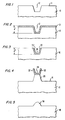
- a semiconductor wafer 10 has located in the surface 11 a depression, such as pit 12.
- the surface 11 is usually referred to as the "top” or “front” surface, being the one in which active devices (transistors, optical devices, etc.) are formed.
- the pit most frequently results from abrasions caused by the above- noted lapping operation, but could be from other sources as well, and are typically distributed over the entire surface of the wafer.
- an etch resistant coating 21 is shown formed on the surface of the wafer.
- the term "etch resistant" refers to having a relatively slow rate of removal as compared to the material of the wafer 10 when subjected to the subsequent isotropic etching operation discussed below.
- coating 21 typically comprises silicon nitride when wafer 10 is silicon, with other materials being possible.
- the formation of the silicon nitride may be by a number of techniques known in the art. One suitable technique is to heat the wafer in a furnace containing a nitrogen ambient.
- silicon nitride deposition rate of about 2.9 nanometers per minute at a pressure of 38.6 Pa (290 millitorr).
- a deposition time of 17 minutes produces a silicon nitride thickness of 50 nanometers.
- silicon nitride thicknesses in the range of 10 to 100 nanometers are suitable for practicing the present invention. It is also possible to include other materials in coating 21. For example, silicon dioxide may be initially formed on the surface 11, followed by the silicon nitride.
- the silicon nitride may also be formed on the back side of the wafer in preparation for a subsequent epitaxial deposition of semiconductor material on the front side.
- the silicon nitride then serves as a "cap" on the back side to prevent autodoping of the front side by dopants outdiffusing from the back side of the wafer.
- One convenient method for forming a silicon dioxide/silicon nitride cap is shown in U. S. Patent 4,687,682 co-assigned with the present invention, with other techniques being possible.
- nitride cap two wafers are loaded in a wafer boat front-to-front (i.e., so that the front sides are in contact), thereby allowing nitride deposition only on the exposed back sides.
- the wafers may be loaded individually into the boat, allowing furnace deposition on both sides.
- the wafers may either be loaded back-to-back, so that the silicon nitride is deposited only on the front sides, or both sides may be coated, with the coating stripped off from the backside after polishing.
- a removal operation removes the etch resistant coating from the high-lying horizontal surface of the wafer, leaving portions 32, 33 on the sidewall of the pit, and portion 34 at the bottom of the pit.
- This removal operation may be performed using a conventional polishing technique in a presently preferred embodiment.
- mechanical polishing with a colloidal silica slurry at a pH of 8.5 for about 1 to 5 minutes is suitable to remove silicon nitride approximately 50 nanometers thick from the high-lying surfaces.
- using polishing to accomplish the removal operation also removes a small thickness of the wafer material, typically about 10 percent of the depth of the coated pits d1 shown in FIG. 2. This has the desirable effect of removing the smaller surface variations (i.e., peaks and valleys) on the wafer.
- the removal may be accomplished by diamond lapping, according to principles known in the art. Still other removal techniques are possible.
- an isotropic etching process is used to remove the surface 11 down to a depth d2 approximating the depth of the pit.
- d2 lies in the range of 5 to 20 micrometers.
- etching in KOH at a temperature of 90 degrees centigrade for about 10 to 20 minutes removes a silicon layer having a thickness in the range of 10 to 20 micrometers.
- the isotropic etching undercuts the protective coating on the sidewalls, so that only regions 32, 33 and 34 remain as viewed in cross-section. Note that the shape of the remaining protective coating is determined by the shape of the pit.
- the basic shape of the pit is influenced by the crystallographic orientation of the wafer. In many cases, the pit is square or rectangular, so that the regions 32-34 are shaped accordingly. The remaining portions of the protective coating become more or less unsupported during etching as wafer material about a pit is removed. It is then possible to readily remove the regions 32-34 by a simple polishing operation.
- a colloidal silica slurry with a pH value in the range of 9.5 to 11.5 is suitable for this subsequent polishing operation.
- polishing with a slurry at a pH of 10 for about 8 to 10 minutes removes a thickness of about 7 micrometers of silicon.
- a short time at the lower pH helps assure a quicker removal of the remaining region 32-34 of the protective coating left behind by the isotropic etching.
- this subsequent polishing operation may still be much shorter than prior art polishing operations, since a protrusion of a given height may be more readily removed than pits of a comparable depth.
- some protrusions are likely to be present if the etching proceeds to the depth of the deepest pit, since the depths of pits on a wafer varies over a range.
- the variations in thickness of a silicon wafer 125 millimeters in diameter were measured to give an indication of flatness.
- the variations were about 1 micrometer, according to the "TTV" measurement.
- the variations increased up to about 8 micrometers.
- using the present inventive technique allowed the polishing time to be reduced sufficiently so that the thickness variations were up to only 2 micrometers.
- the exemplary values above are for an aluminum oxide abrasive slurry having a nominal grain size of 12 micrometers.
- the present invention may be practiced with other abrasives and grain sizes, with the appropriate changes to the values given.
- the present invention may also be practiced on surfaces obtained from mechanical preparation techniques other than lapping.
- the wafer instead of being lapped on both sides, the wafer may be ground (e.g., on a bonded diamond wheel) or sawed on both sides. Alternately, the wafer may be lapped on one side and ground or sawed on the other, or ground on one side and sawed on the other.
- the mechanical preparation may optionally be followed by chemical etching, as discussed above.
- the present invention is also applicable to wafers to be polished on both sides.
- both sides may be coated with an etch-resistant material, and both sides may be polished and etched as described above.
- the inventive treatment of the two sides may be practiced either simultaneously or sequentially.
- silicon dioxide may be used as the etch resistant material.
- Polymer coatings e.g., lithographic resists
- isotropic etchants for example a solution of sodium hydroxide, may be used to remove silicon in the step shown in FIG. 4.
- Germanium and III-V semiconductor wafers may advantageously utilize the present technique with the appropriate choice of etch resistant material and wafer etching techniques.
- quartz i.e., single crystal or fused silica
- glass wafers may utilize the present technique.
- etch resistant protective coating aluminum oxide may be used as the etch resistant protective coating, and hydrofluoric acid (HF), or other fluoride-containing solutions, as the isotropic etchant.
- HF hydrofluoric acid
- the present technique may be practiced with a wafer of any brittle material.
- sawing with a diamond tipped blade is the presently preferred technique for separating a wafer from an ingot, other techniques are possible, including, for example, the use of high pressure water jets, wire sawing, laser cutting, etc.
- integrated circuits are typically formed on the wafer using lithography techniques that advantageously utilize the improved flatness obtained thereby.
- lithography techniques that advantageously utilize the improved flatness obtained thereby.
- the value of the present invention is not limited to the wafer production process per se , but rather extends to the integrated circuit production process.
- the various lithography operations are well-known in the art, and need not be recited herein. Still other operations in the integrated circuit production process may benefit from the practice of the present invention, including deposition, etching, and planarization techniques.
Applications Claiming Priority (2)
| Application Number | Priority Date | Filing Date | Title |
|---|---|---|---|
| US07/290,653 US4874463A (en) | 1988-12-23 | 1988-12-23 | Integrated circuits from wafers having improved flatness |
| US290653 | 1988-12-23 |
Publications (3)
| Publication Number | Publication Date |
|---|---|
| EP0375258A2 EP0375258A2 (en) | 1990-06-27 |
| EP0375258A3 EP0375258A3 (en) | 1991-03-20 |
| EP0375258B1 true EP0375258B1 (en) | 1994-06-22 |
Family
ID=23116985
Family Applications (1)
| Application Number | Title | Priority Date | Filing Date |
|---|---|---|---|
| EP89313008A Expired - Lifetime EP0375258B1 (en) | 1988-12-23 | 1989-12-13 | Method of fabricating a flat wafer |
Country Status (6)
| Country | Link |
|---|---|
| US (1) | US4874463A (ja) |
| EP (1) | EP0375258B1 (ja) |
| JP (1) | JPH069194B2 (ja) |
| DE (1) | DE68916393T2 (ja) |
| ES (1) | ES2056232T3 (ja) |
| HK (1) | HK135295A (ja) |
Families Citing this family (19)
| Publication number | Priority date | Publication date | Assignee | Title |
|---|---|---|---|---|
| US6391798B1 (en) | 1987-02-27 | 2002-05-21 | Agere Systems Guardian Corp. | Process for planarization a semiconductor substrate |
| EP0368584B1 (en) * | 1988-11-09 | 1997-03-19 | Sony Corporation | Method of manufacturing a semiconductor wafer |
| GB2227362B (en) * | 1989-01-18 | 1992-11-04 | Gen Electric Co Plc | Electronic devices |
| US5142828A (en) * | 1990-06-25 | 1992-09-01 | Microelectronics And Computer Technology Corporation | Correcting a defective metallization layer on an electronic component by polishing |
| US5137597A (en) * | 1991-04-11 | 1992-08-11 | Microelectronics And Computer Technology Corporation | Fabrication of metal pillars in an electronic component using polishing |
| EP0529888A1 (en) * | 1991-08-22 | 1993-03-03 | AT&T Corp. | Removal of substrate perimeter material |
| EP0619495B1 (de) * | 1993-04-05 | 1997-05-21 | Siemens Aktiengesellschaft | Verfahren zur Herstellung von Tunneleffekt-Sensoren |
| US5356513A (en) * | 1993-04-22 | 1994-10-18 | International Business Machines Corporation | Polishstop planarization method and structure |
| US5473433A (en) * | 1993-12-07 | 1995-12-05 | At&T Corp. | Method of high yield manufacture of VLSI type integrated circuit devices by determining critical surface characteristics of mounting films |
| US5733175A (en) * | 1994-04-25 | 1998-03-31 | Leach; Michael A. | Polishing a workpiece using equal velocity at all points overlapping a polisher |
| US5607341A (en) | 1994-08-08 | 1997-03-04 | Leach; Michael A. | Method and structure for polishing a wafer during manufacture of integrated circuits |
| US5885900A (en) * | 1995-11-07 | 1999-03-23 | Lucent Technologies Inc. | Method of global planarization in fabricating integrated circuit devices |
| US5766971A (en) * | 1996-12-13 | 1998-06-16 | International Business Machines Corporation | Oxide strip that improves planarity |
| US6514875B1 (en) | 1997-04-28 | 2003-02-04 | The Regents Of The University Of California | Chemical method for producing smooth surfaces on silicon wafers |
| US6019806A (en) * | 1998-01-08 | 2000-02-01 | Sees; Jennifer A. | High selectivity slurry for shallow trench isolation processing |
| CN1347566A (zh) * | 1999-04-16 | 2002-05-01 | 东京电子株式会社 | 半导体器件的制造方法及其制造生产线 |
| US6600557B1 (en) * | 1999-05-21 | 2003-07-29 | Memc Electronic Materials, Inc. | Method for the detection of processing-induced defects in a silicon wafer |
| US6416391B1 (en) | 2000-02-28 | 2002-07-09 | Seh America, Inc. | Method of demounting silicon wafers after polishing |
| US6446948B1 (en) | 2000-03-27 | 2002-09-10 | International Business Machines Corporation | Vacuum chuck for reducing distortion of semiconductor and GMR head wafers during processing |
Family Cites Families (6)
| Publication number | Priority date | Publication date | Assignee | Title |
|---|---|---|---|---|
| US4278987A (en) * | 1977-10-17 | 1981-07-14 | Hitachi, Ltd. | Junction isolated IC with thick EPI portion having sides at least 20 degrees from (110) orientations |
| US4331546A (en) * | 1979-01-31 | 1982-05-25 | Mobil Oil Corporation | Lubricant composition containing phosphite-diarylamine-carbonyl compound reaction product |
| US4251300A (en) * | 1979-05-14 | 1981-02-17 | Fairchild Camera And Instrument Corporation | Method for forming shaped buried layers in semiconductor devices utilizing etching, epitaxial deposition and oxide formation |
| US4588421A (en) * | 1984-10-15 | 1986-05-13 | Nalco Chemical Company | Aqueous silica compositions for polishing silicon wafers |
| US4671851A (en) * | 1985-10-28 | 1987-06-09 | International Business Machines Corporation | Method for removing protuberances at the surface of a semiconductor wafer using a chem-mech polishing technique |
| US4735679A (en) * | 1987-03-30 | 1988-04-05 | International Business Machines Corporation | Method of improving silicon-on-insulator uniformity |
-
1988
- 1988-12-23 US US07/290,653 patent/US4874463A/en not_active Expired - Lifetime
-
1989
- 1989-12-13 EP EP89313008A patent/EP0375258B1/en not_active Expired - Lifetime
- 1989-12-13 DE DE68916393T patent/DE68916393T2/de not_active Expired - Lifetime
- 1989-12-13 ES ES89313008T patent/ES2056232T3/es not_active Expired - Lifetime
- 1989-12-22 JP JP1331425A patent/JPH069194B2/ja not_active Expired - Lifetime
-
1995
- 1995-08-24 HK HK135295A patent/HK135295A/xx not_active IP Right Cessation
Also Published As
| Publication number | Publication date |
|---|---|
| ES2056232T3 (es) | 1994-10-01 |
| DE68916393D1 (de) | 1994-07-28 |
| EP0375258A2 (en) | 1990-06-27 |
| DE68916393T2 (de) | 1994-12-22 |
| JPH02226723A (ja) | 1990-09-10 |
| US4874463A (en) | 1989-10-17 |
| HK135295A (en) | 1995-09-01 |
| JPH069194B2 (ja) | 1994-02-02 |
| EP0375258A3 (en) | 1991-03-20 |
Similar Documents
| Publication | Publication Date | Title |
|---|---|---|
| EP0375258B1 (en) | Method of fabricating a flat wafer | |
| EP2267189B1 (en) | High surface quality gan wafer and method of fabricating same | |
| JP2910507B2 (ja) | 半導体ウエーハの製造方法 | |
| US6376335B1 (en) | Semiconductor wafer manufacturing process | |
| EP0854500A1 (en) | Method of manufacturing a bonding substrate | |
| JP2006222453A (ja) | シリコンウエーハの製造方法及びシリコンウエーハ並びにsoiウエーハ | |
| JP2008227534A (ja) | SiC基板 | |
| JP4148105B2 (ja) | SiC基板の製造方法 | |
| US5899731A (en) | Method of fabricating a semiconductor wafer | |
| JP3446616B2 (ja) | シリコンウエーハのエッチング方法およびシリコンウエーハ用エッチング液 | |
| JPH10223497A (ja) | 貼り合わせ基板の作製方法 | |
| US3738882A (en) | Method for polishing semiconductor gallium arsenide planar surfaces | |
| EP0860862A2 (en) | Method of manufacturing a bonding substrate | |
| JP2009147104A (ja) | 使用済み半導体ウエハ又は基板の再生方法 | |
| US6063301A (en) | Crystal display processing method and crystal wafer manufacturing method | |
| JPH06112173A (ja) | 半導体シリコンエピタキシャル基板の製造方法 | |
| KR101086966B1 (ko) | 반도체 웨이퍼 연마방법 | |
| JP2000286173A (ja) | ハードレーザマーキングウェーハおよびその製造方法 | |
| KR100398704B1 (ko) | 실리콘 웨이퍼 제조 방법 | |
| JP2000211997A (ja) | エピタキシャルウェ―ハの製造方法 | |
| JPH09306897A (ja) | シリコンウェーハ表面粗さ制御用のエッチャント | |
| JP3578238B2 (ja) | シリコンウェーハの加工方法 | |
| JP2778114B2 (ja) | 半導体基板の製法 | |
| JP2001223163A (ja) | シリコンエピタキシャルウェーハ及びその製造方法 | |
| JPH11340443A (ja) | Soiウエーハの作製方法およびsoiウエーハ |
Legal Events
| Date | Code | Title | Description |
|---|---|---|---|
| PUAI | Public reference made under article 153(3) epc to a published international application that has entered the european phase |
Free format text: ORIGINAL CODE: 0009012 |
|
| AK | Designated contracting states |
Kind code of ref document: A2 Designated state(s): DE ES FR GB IT NL |
|
| PUAL | Search report despatched |
Free format text: ORIGINAL CODE: 0009013 |
|
| AK | Designated contracting states |
Kind code of ref document: A3 Designated state(s): DE ES FR GB IT NL |
|
| 17P | Request for examination filed |
Effective date: 19910912 |
|
| 17Q | First examination report despatched |
Effective date: 19931110 |
|
| GRAA | (expected) grant |
Free format text: ORIGINAL CODE: 0009210 |
|
| AK | Designated contracting states |
Kind code of ref document: B1 Designated state(s): DE ES FR GB IT NL |
|
| RAP3 | Party data changed (applicant data changed or rights of an application transferred) |
Owner name: AT&T CORP. |
|
| ET | Fr: translation filed | ||
| REF | Corresponds to: |
Ref document number: 68916393 Country of ref document: DE Date of ref document: 19940728 |
|
| ITF | It: translation for a ep patent filed |
Owner name: JACOBACCI CASETTA & PERANI S.P.A. |
|
| REG | Reference to a national code |
Ref country code: ES Ref legal event code: FG2A Ref document number: 2056232 Country of ref document: ES Kind code of ref document: T3 |
|
| PLBE | No opposition filed within time limit |
Free format text: ORIGINAL CODE: 0009261 |
|
| STAA | Information on the status of an ep patent application or granted ep patent |
Free format text: STATUS: NO OPPOSITION FILED WITHIN TIME LIMIT |
|
| 26N | No opposition filed | ||
| PGFP | Annual fee paid to national office [announced via postgrant information from national office to epo] |
Ref country code: FR Payment date: 19991124 Year of fee payment: 11 |
|
| PGFP | Annual fee paid to national office [announced via postgrant information from national office to epo] |
Ref country code: GB Payment date: 19991126 Year of fee payment: 11 |
|
| PGFP | Annual fee paid to national office [announced via postgrant information from national office to epo] |
Ref country code: NL Payment date: 19991129 Year of fee payment: 11 |
|
| PGFP | Annual fee paid to national office [announced via postgrant information from national office to epo] |
Ref country code: ES Payment date: 19991210 Year of fee payment: 11 |
|
| PG25 | Lapsed in a contracting state [announced via postgrant information from national office to epo] |
Ref country code: GB Free format text: LAPSE BECAUSE OF NON-PAYMENT OF DUE FEES Effective date: 20001213 |
|
| PG25 | Lapsed in a contracting state [announced via postgrant information from national office to epo] |
Ref country code: NL Free format text: LAPSE BECAUSE OF NON-PAYMENT OF DUE FEES Effective date: 20010701 |
|
| GBPC | Gb: european patent ceased through non-payment of renewal fee |
Effective date: 20001213 |
|
| PG25 | Lapsed in a contracting state [announced via postgrant information from national office to epo] |
Ref country code: FR Free format text: LAPSE BECAUSE OF NON-PAYMENT OF DUE FEES Effective date: 20010831 |
|
| NLV4 | Nl: lapsed or anulled due to non-payment of the annual fee |
Effective date: 20010701 |
|
| REG | Reference to a national code |
Ref country code: FR Ref legal event code: ST |
|
| PG25 | Lapsed in a contracting state [announced via postgrant information from national office to epo] |
Ref country code: ES Free format text: LAPSE BECAUSE OF NON-PAYMENT OF DUE FEES Effective date: 20011214 |
|
| PGFP | Annual fee paid to national office [announced via postgrant information from national office to epo] |
Ref country code: DE Payment date: 20011230 Year of fee payment: 13 |
|
| PG25 | Lapsed in a contracting state [announced via postgrant information from national office to epo] |
Ref country code: DE Free format text: LAPSE BECAUSE OF NON-PAYMENT OF DUE FEES Effective date: 20030701 |
|
| REG | Reference to a national code |
Ref country code: ES Ref legal event code: FD2A Effective date: 20020112 |
|
| PG25 | Lapsed in a contracting state [announced via postgrant information from national office to epo] |
Ref country code: IT Free format text: LAPSE BECAUSE OF NON-PAYMENT OF DUE FEES;WARNING: LAPSES OF ITALIAN PATENTS WITH EFFECTIVE DATE BEFORE 2007 MAY HAVE OCCURRED AT ANY TIME BEFORE 2007. THE CORRECT EFFECTIVE DATE MAY BE DIFFERENT FROM THE ONE RECORDED. Effective date: 20051213 |