EP0374286B1 - Verfahren zur Herstellung einer gedruckten Zweischicht-Schaltungsplatte - Google Patents
Verfahren zur Herstellung einer gedruckten Zweischicht-Schaltungsplatte Download PDFInfo
- Publication number
- EP0374286B1 EP0374286B1 EP88121390A EP88121390A EP0374286B1 EP 0374286 B1 EP0374286 B1 EP 0374286B1 EP 88121390 A EP88121390 A EP 88121390A EP 88121390 A EP88121390 A EP 88121390A EP 0374286 B1 EP0374286 B1 EP 0374286B1
- Authority
- EP
- European Patent Office
- Prior art keywords
- sheet
- hole
- layer
- insulating sheet
- conductive paste
- Prior art date
- Legal status (The legal status is an assumption and is not a legal conclusion. Google has not performed a legal analysis and makes no representation as to the accuracy of the status listed.)
- Expired - Lifetime
Links
- 238000004519 manufacturing process Methods 0.000 title claims description 11
- 238000007639 printing Methods 0.000 claims description 13
- 238000000034 method Methods 0.000 claims description 11
- 239000011347 resin Substances 0.000 claims description 9
- 229920005989 resin Polymers 0.000 claims description 9
- -1 polyethylene terephthalate Polymers 0.000 claims description 3
- 229920000139 polyethylene terephthalate Polymers 0.000 claims description 3
- 239000005020 polyethylene terephthalate Substances 0.000 claims description 3
- 238000005476 soldering Methods 0.000 claims description 3
- 229920001721 polyimide Polymers 0.000 claims description 2
- 239000011342 resin composition Substances 0.000 claims 2
- 230000001464 adherent effect Effects 0.000 claims 1
- XLYOFNOQVPJJNP-UHFFFAOYSA-N water Substances O XLYOFNOQVPJJNP-UHFFFAOYSA-N 0.000 claims 1
- 239000010410 layer Substances 0.000 description 37
- BQCADISMDOOEFD-UHFFFAOYSA-N Silver Chemical compound [Ag] BQCADISMDOOEFD-UHFFFAOYSA-N 0.000 description 7
- 238000001746 injection moulding Methods 0.000 description 7
- 229910052709 silver Inorganic materials 0.000 description 7
- 239000004332 silver Substances 0.000 description 7
- 239000000853 adhesive Substances 0.000 description 3
- 239000011229 interlayer Substances 0.000 description 3
- 229910052751 metal Inorganic materials 0.000 description 3
- 239000002184 metal Substances 0.000 description 3
- 238000007650 screen-printing Methods 0.000 description 3
- 238000012546 transfer Methods 0.000 description 3
- PXHVJJICTQNCMI-UHFFFAOYSA-N Nickel Chemical compound [Ni] PXHVJJICTQNCMI-UHFFFAOYSA-N 0.000 description 2
- HCHKCACWOHOZIP-UHFFFAOYSA-N Zinc Chemical compound [Zn] HCHKCACWOHOZIP-UHFFFAOYSA-N 0.000 description 2
- 229910052782 aluminium Inorganic materials 0.000 description 2
- XAGFODPZIPBFFR-UHFFFAOYSA-N aluminium Chemical compound [Al] XAGFODPZIPBFFR-UHFFFAOYSA-N 0.000 description 2
- 239000003795 chemical substances by application Substances 0.000 description 2
- 239000011248 coating agent Substances 0.000 description 2
- 238000000576 coating method Methods 0.000 description 2
- 238000009413 insulation Methods 0.000 description 2
- 238000013508 migration Methods 0.000 description 2
- 230000005012 migration Effects 0.000 description 2
- 229920002379 silicone rubber Polymers 0.000 description 2
- 239000004945 silicone rubber Substances 0.000 description 2
- 229910000679 solder Inorganic materials 0.000 description 2
- 229910052725 zinc Inorganic materials 0.000 description 2
- 239000011701 zinc Substances 0.000 description 2
- RYGMFSIKBFXOCR-UHFFFAOYSA-N Copper Chemical compound [Cu] RYGMFSIKBFXOCR-UHFFFAOYSA-N 0.000 description 1
- 239000012790 adhesive layer Substances 0.000 description 1
- 239000012670 alkaline solution Substances 0.000 description 1
- BGTFCAQCKWKTRL-YDEUACAXSA-N chembl1095986 Chemical compound C1[C@@H](N)[C@@H](O)[C@H](C)O[C@H]1O[C@@H]([C@H]1C(N[C@H](C2=CC(O)=CC(O[C@@H]3[C@H]([C@@H](O)[C@H](O)[C@@H](CO)O3)O)=C2C=2C(O)=CC=C(C=2)[C@@H](NC(=O)[C@@H]2NC(=O)[C@@H]3C=4C=C(C(=C(O)C=4)C)OC=4C(O)=CC=C(C=4)[C@@H](N)C(=O)N[C@@H](C(=O)N3)[C@H](O)C=3C=CC(O4)=CC=3)C(=O)N1)C(O)=O)=O)C(C=C1)=CC=C1OC1=C(O[C@@H]3[C@H]([C@H](O)[C@@H](O)[C@H](CO[C@@H]5[C@H]([C@@H](O)[C@H](O)[C@@H](C)O5)O)O3)O[C@@H]3[C@H]([C@@H](O)[C@H](O)[C@@H](CO)O3)O[C@@H]3[C@H]([C@H](O)[C@@H](CO)O3)O)C4=CC2=C1 BGTFCAQCKWKTRL-YDEUACAXSA-N 0.000 description 1
- 238000007796 conventional method Methods 0.000 description 1
- 229910052802 copper Inorganic materials 0.000 description 1
- 239000010949 copper Substances 0.000 description 1
- 230000003247 decreasing effect Effects 0.000 description 1
- 239000000945 filler Substances 0.000 description 1
- 239000000463 material Substances 0.000 description 1
- 238000012986 modification Methods 0.000 description 1
- 230000004048 modification Effects 0.000 description 1
- 229910052759 nickel Inorganic materials 0.000 description 1
- 239000002987 primer (paints) Substances 0.000 description 1
- 230000003014 reinforcing effect Effects 0.000 description 1
- 239000002356 single layer Substances 0.000 description 1
- 238000005507 spraying Methods 0.000 description 1
- 239000000758 substrate Substances 0.000 description 1
Images

Classifications
-
- H—ELECTRICITY
- H05—ELECTRIC TECHNIQUES NOT OTHERWISE PROVIDED FOR
- H05K—PRINTED CIRCUITS; CASINGS OR CONSTRUCTIONAL DETAILS OF ELECTRIC APPARATUS; MANUFACTURE OF ASSEMBLAGES OF ELECTRICAL COMPONENTS
- H05K3/00—Apparatus or processes for manufacturing printed circuits
- H05K3/40—Forming printed elements for providing electric connections to or between printed circuits
- H05K3/4038—Through-connections; Vertical interconnect access [VIA] connections
- H05K3/4053—Through-connections; Vertical interconnect access [VIA] connections by thick-film techniques
- H05K3/4069—Through-connections; Vertical interconnect access [VIA] connections by thick-film techniques for via connections in organic insulating substrates
-
- H—ELECTRICITY
- H05—ELECTRIC TECHNIQUES NOT OTHERWISE PROVIDED FOR
- H05K—PRINTED CIRCUITS; CASINGS OR CONSTRUCTIONAL DETAILS OF ELECTRIC APPARATUS; MANUFACTURE OF ASSEMBLAGES OF ELECTRICAL COMPONENTS
- H05K1/00—Printed circuits
- H05K1/02—Details
- H05K1/03—Use of materials for the substrate
- H05K1/0393—Flexible materials
-
- H—ELECTRICITY
- H05—ELECTRIC TECHNIQUES NOT OTHERWISE PROVIDED FOR
- H05K—PRINTED CIRCUITS; CASINGS OR CONSTRUCTIONAL DETAILS OF ELECTRIC APPARATUS; MANUFACTURE OF ASSEMBLAGES OF ELECTRICAL COMPONENTS
- H05K1/00—Printed circuits
- H05K1/02—Details
- H05K1/09—Use of materials for the conductive, e.g. metallic pattern
- H05K1/092—Dispersed materials, e.g. conductive pastes or inks
- H05K1/095—Dispersed materials, e.g. conductive pastes or inks for polymer thick films, i.e. having a permanent organic polymeric binder
-
- H—ELECTRICITY
- H05—ELECTRIC TECHNIQUES NOT OTHERWISE PROVIDED FOR
- H05K—PRINTED CIRCUITS; CASINGS OR CONSTRUCTIONAL DETAILS OF ELECTRIC APPARATUS; MANUFACTURE OF ASSEMBLAGES OF ELECTRICAL COMPONENTS
- H05K2203/00—Indexing scheme relating to apparatus or processes for manufacturing printed circuits covered by H05K3/00
- H05K2203/01—Tools for processing; Objects used during processing
- H05K2203/0147—Carriers and holders
- H05K2203/0156—Temporary polymeric carrier or foil, e.g. for processing or transferring
-
- H—ELECTRICITY
- H05—ELECTRIC TECHNIQUES NOT OTHERWISE PROVIDED FOR
- H05K—PRINTED CIRCUITS; CASINGS OR CONSTRUCTIONAL DETAILS OF ELECTRIC APPARATUS; MANUFACTURE OF ASSEMBLAGES OF ELECTRICAL COMPONENTS
- H05K2203/00—Indexing scheme relating to apparatus or processes for manufacturing printed circuits covered by H05K3/00
- H05K2203/07—Treatments involving liquids, e.g. plating, rinsing
- H05K2203/0756—Uses of liquids, e.g. rinsing, coating, dissolving
- H05K2203/0769—Dissolving insulating materials, e.g. coatings, not used for developing resist after exposure
-
- H—ELECTRICITY
- H05—ELECTRIC TECHNIQUES NOT OTHERWISE PROVIDED FOR
- H05K—PRINTED CIRCUITS; CASINGS OR CONSTRUCTIONAL DETAILS OF ELECTRIC APPARATUS; MANUFACTURE OF ASSEMBLAGES OF ELECTRICAL COMPONENTS
- H05K2203/00—Indexing scheme relating to apparatus or processes for manufacturing printed circuits covered by H05K3/00
- H05K2203/14—Related to the order of processing steps
- H05K2203/1453—Applying the circuit pattern before another process, e.g. before filling of vias with conductive paste, before making printed resistors
-
- H—ELECTRICITY
- H05—ELECTRIC TECHNIQUES NOT OTHERWISE PROVIDED FOR
- H05K—PRINTED CIRCUITS; CASINGS OR CONSTRUCTIONAL DETAILS OF ELECTRIC APPARATUS; MANUFACTURE OF ASSEMBLAGES OF ELECTRICAL COMPONENTS
- H05K2203/00—Indexing scheme relating to apparatus or processes for manufacturing printed circuits covered by H05K3/00
- H05K2203/14—Related to the order of processing steps
- H05K2203/1476—Same or similar kind of process performed in phases, e.g. coarse patterning followed by fine patterning
-
- H—ELECTRICITY
- H05—ELECTRIC TECHNIQUES NOT OTHERWISE PROVIDED FOR
- H05K—PRINTED CIRCUITS; CASINGS OR CONSTRUCTIONAL DETAILS OF ELECTRIC APPARATUS; MANUFACTURE OF ASSEMBLAGES OF ELECTRICAL COMPONENTS
- H05K3/00—Apparatus or processes for manufacturing printed circuits
- H05K3/22—Secondary treatment of printed circuits
- H05K3/28—Applying non-metallic protective coatings
-
- Y—GENERAL TAGGING OF NEW TECHNOLOGICAL DEVELOPMENTS; GENERAL TAGGING OF CROSS-SECTIONAL TECHNOLOGIES SPANNING OVER SEVERAL SECTIONS OF THE IPC; TECHNICAL SUBJECTS COVERED BY FORMER USPC CROSS-REFERENCE ART COLLECTIONS [XRACs] AND DIGESTS
- Y10—TECHNICAL SUBJECTS COVERED BY FORMER USPC
- Y10S—TECHNICAL SUBJECTS COVERED BY FORMER USPC CROSS-REFERENCE ART COLLECTIONS [XRACs] AND DIGESTS
- Y10S428/00—Stock material or miscellaneous articles
- Y10S428/901—Printed circuit
-
- Y—GENERAL TAGGING OF NEW TECHNOLOGICAL DEVELOPMENTS; GENERAL TAGGING OF CROSS-SECTIONAL TECHNOLOGIES SPANNING OVER SEVERAL SECTIONS OF THE IPC; TECHNICAL SUBJECTS COVERED BY FORMER USPC CROSS-REFERENCE ART COLLECTIONS [XRACs] AND DIGESTS
- Y10—TECHNICAL SUBJECTS COVERED BY FORMER USPC
- Y10T—TECHNICAL SUBJECTS COVERED BY FORMER US CLASSIFICATION
- Y10T29/00—Metal working
- Y10T29/49—Method of mechanical manufacture
- Y10T29/49002—Electrical device making
- Y10T29/49117—Conductor or circuit manufacturing
- Y10T29/49124—On flat or curved insulated base, e.g., printed circuit, etc.
- Y10T29/49155—Manufacturing circuit on or in base
- Y10T29/49165—Manufacturing circuit on or in base by forming conductive walled aperture in base
Definitions
- the present invention relates to a method of manufacturing a printed circuit sheet having a two-layer circuit pattern.
- a circuit pattern transfer sheet is placed in an injection molding die, and a circuit pattern is integrally formed on a required surface of an injection-molded body simultaneously with injection molding.
- the circuit pattern transfer sheet in this method is obtained by printing a circuit pattern on a releasable base sheet by using a conductive paste, and forming an adhesive layer for adhesion with the injection-molded body thereon.
- a circuit pattern is formed in a single layer.
- circuit patterns must be formed in two layers.
- circuit patterns are to be printed in two layers by using a conductive paste, the following method is employed.
- a first-layer circuit pattern is printed on a base sheet using a conductive paste, thereafter an insulating layer consisting of an insulating paste, and through studs (for electrically connecting circuit patterns of two layers to each other) are printed overlapping the first-layer circuit pattern.
- a second-layer circuit pattern is printed on the resultant structure by using a conductive paste.
- an insulating layer for insulating circuit patterns of two layers is formed by screen printing using an insulating paste, in order to obtain a sufficient thickness (60 »m or more) of the insulating layer, printing must be performed three times or more. As a result, the number of steps and hence the cost are increased. In addition, since printing is performed a plurality of times, variations in layer thickness tend to occur and voids are easily generated. Therefore, reliability of interlayer insulation is insufficient.
- a silver paste is generally used as a conductive paste. However, if the silver paste is printed on an insulating paste, migration of silver tends to occur.
- US-A-4 263 341 discloses a method of making two-sided boards with metal through-hole connects.
- a primer coating of a metal such as zinc is sprayed onto one surface of the substrate, through a chrome-plated metal stencil , after which a conductive coating, such as copper or nickel, is sprayed onto the zinc coating to form the conductive patterns.
- Through hole connections are fabricated by forming tapered holes , and placing a removable stop member against the narrow end of the hole before spraying the patterns. The first pattern is then sprayed on from the wide end of the hole so that a portion of the material coats the walls of the hole and forms a bridging strip across the narrow end of the hole. After this, the stop is removed, and the other side is sprayed to form a conductive portion contacting the bridging strip to make the through connect.
- the present invention has been made to solve the above problems, and has as its object to provide a method of manufacturing a two-layer printed circuit sheet, in which an insulating layer can be obtained without screen printing, and the steps are simplified.
- a method of manufacturing a two-layer printed circuit sheet comprising the steps of preparing an insulating sheet, on both surfaces of which circuit patterns are to be formed, the insulating sheet having a through hole formed therein in advance at a position where the circuit patterns are to be electrically connected to each other, forming a bottom of the through hole by attaching a releasable hole-bottom sheet to one of the surfaces of the insulating sheet, filling, as a separate step, a conductive paste into the through hole from an open end thereof, printing a first-layer circuit pattern on the other surface of the insulating sheet to which the hole-bottom sheet is not attached, removing the hole bottom sheet, and printing a second-layer circuit pattern on the surface of the insulating sheet, from which the hole bottom sheet is removed.
- circuit patterns are printed on both the surfaces of the insulating sheet in this manner so that the thickness of the insulating layer can be made uniform. As a result, reliability of interlayer insulation can be increased, and the number of printing steps can be decreased.
- a through hole is formed in the insulating sheet in advance, and a hole bottom sheet is attached to one surface of the insulating sheet. Subsequently, a conductive paste is filled into the hole, and then the hole bottom sheet is removed. With this process, the through hole of the insulating sheet can be completely filled with the conductive paste, and hence the circuit patterns on both the surfaces can be reliably rendered conductive.
- a two-layer printed circuit sheet according to the present invention is defined in claim 9.
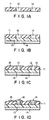
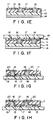
- Figs. 1A to 1H show steps in an embodiment of the present invention.
- insulating sheet 11 is prepared.
- Insulating sheet 11 has through holes 12 at positions for electrically connecting circuit patterns formed on its both surfaces.
- a resin film such as a polyethylene terephthalate film or a polyimide film, having a thickness of about 50 »m is used as insulating film 11.
- hole-bottom sheet 13 is attached to one surface of insulating sheet 11 so as to form hole bottoms.
- Hole-bottom sheet 13 is made of a water-soluble resin film.
- Hole-bottom sheet 13 is attached to reinforcing sheet 14 made of, for example, aluminum.
- RISTON ® available from Du Pont de Nemours can be used as the water-soluble resin film constituting hole-bottom sheet 13.
- first-layer circuit pattern 15 is printed on the other surface of insulating sheet 11 by using a conductive paste containing a silver filler. Upon this printing, the conductive paste is dropped in holes 12. However, since holes 12 cannot be completely filled with the conductive paste by only this operation, conductive paste 16 is further printed for filling holes 12, as shown in Fig. 1D.
- the conductive paste for circuit pattern 15 may be used as hole-filling conductive paste 16. In this embodiment, however, since conductive pastes 16 in these holes are formed into pad portions for mounting parts, a conductive paste (land paste) allowing soldering is used.
- solder resist 17 is printed except for the pad portions.
- release agent 18 for transferring circuit pattern is coated on the resultant structure, and carrier film 19 is then attached thereto. Thereafter, aluminum sheet 14 is peeled off, and water-soluble resin film 13 is removed by using an aqueous alkaline solution, thereby exposing insulating sheet 11.
- second-layer circuit pattern 20 is printed on exposed insulating sheet 11 by using a silver paste, as shown in Fig. 1G. Furthermore, as shown in Fig. 1H, adhesive agent 21 is coated on pattern 20. Adhesive agent 21 increases adherence between the printed circuit sheet manufactured in this manner and an injection molding resin to be integrally formed with the sheet.
- a transfer sheet having circuit patterns of two layers is completed.
- This sheet is set in a die such that the adhesive agent 21 is brought into contact with the injection molding resin.
- carrier film 19 is peeled off together with release agent 18 upon injection molding, an injection-molded body with which the two-layer printed circuit sheet is integrally formed can be obtained.
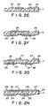
- Figs. 2A to 2H show another embodiment of the present invention. Similar to the above-described embodiment, insulating film 11 having through holes 12 formed therein at its predetermined positions is prepared, as shown in Fig. 2A. Thereafter, as shown in Fig. 2B, hole-bottom sheet 23 made of silicone rubber is attached to one surface of insulating sheet 11 so as to form hole bottoms. A sheet having such adherence as to allow the sheet to be easily peeled off later is used as sheet 23.
- conductive paste 24 is filled into each hole 12 from the other surface of insulating sheet 11 by screen printing.
- first-layer circuit pattern 25 is printed on the resultant structure by using a conductive paste, as shown in Fig. 2D.
- Sheet 23 is then peeled off to obtain a state shown in Fig. 2E.
- the resultant structure is turned upside down, and second-layer circuit pattern 26 is printed on insulating sheet 11 by using a conductive paste, as shown in Fig. 2F.
- conductive paste 27 allowing soldering is printed on part-mounting portions of second-layer circuit pattern 26, thereby forming pad portions.
- solder resist 28 is printed except for the pad portions, as shown in Fig. 2H.
- a two-layer printed circuit sheet is completed.
- this sheet is set in a die such that the first-layer circuit pattern 25 side is brought into contact with an injection molding resin, and injection molding is performed, an injection-molded body incorporating the two-layer printed circuit sheet can be obtained.
- the thickness of an insulating layer between the circuit patterns of the two layers can be made uniform, and the number of printing steps can be deceased.
- through holes formed in an insulating sheet in advance can be completely filled with a conductive paste at conductive portions of the circuit patterns of the two layers by using a hole bottom sheet, a highly reliable conductive state can be obtained.
- a silver paste is used as a conductive paste for a circuit pattern, since an interlayer insulating layer consists of an insulating sheet instead of a paste, occurrence of silver migration is suppressed.
- a two-layer printed circuit sheet obtained by the manufacturing method of the present invention is suitable to be used integrally with an injection-molded body, its application is not limited to this.
- this sheet can be independently used.
- the present invention is not limited to the above embodiments, and various changes and modifications can be made.
- a polyethylene terephthalate film or the like is used as an insulating sheet in the embodiments.
- the present invention is not limited to this.
- a water-soluble resin film or silicone rubber is used as a hole-bottom sheet.
- the present invention is not limited to this.
Landscapes
- Engineering & Computer Science (AREA)
- Manufacturing & Machinery (AREA)
- Microelectronics & Electronic Packaging (AREA)
- Printing Elements For Providing Electric Connections Between Printed Circuits (AREA)
- Manufacturing Of Printed Wiring (AREA)
Claims (9)
- Verfahren zum Herstellen eines zweischichtigen, gedruckten Schaltungsblattes, das folgende Schritte aufweist:
Herstellen eines isolierenden Blattes (11), auf dessen beiden Oberflächen Schaltungsmuster gebildet werden sollen, wobei das isolierende Blatt (11) ein darin gebildetes Durchgangsloch (12) an einer Stelle aufweist, an der die Schaltungsmuster elektrisch miteinander verbunden werden sollen;
Bilden eines Bodens des Durchgangsloches (12) durch Befestigen eines ablösbaren Bodenlochblattes (13, 23) auf einer der Oberflächen des isolierenden Blattes (11);
Einfüllen einer leitenden Paste (16, 24) in das Durchgangsloch (12) vom offenen Ende desselben her, als separater Schritt;
Drucken eines Erstschicht-Schaltungsmusters (15, 25) auf die andere Oberfläche des isolierenden Blattes (11), auf dem das Lochbodenblatt (18, 23) nicht befestigt wird;
Beseitigen des Lochbodenblattes (13, 23); und
Drucken eines Zweitschicht-Schaltungsmusters (20, 26) auf die Oberfläche des isolierenden Blattes (11), von der das Lochbodenblatt (13) entfernt wird. - Verfahren nach Anspruch 1, dadurch gekennzeichnet, daß das Lochbodenblatt (13) eine wasserlösliche Harzverbindung umfaßt und durch Auflösen der Harzverbindung in Wasser beseitigt wird.
- Verfahren nach Anspruch 1, dadurch gekennzeichnet, daß das Lochbodenblatt (23) ein haltendes Blatt umfaßt und durch Abschälen entfernt wird.
- Verfahren nach Anspruch 1, dadurch gekennzeichnet, daß der Schritt des Einfüllens der leitenden Paste (16) in das Durchgangsloch (12) nach dem Aufdrucken des Erstschicht-Schaltungsmusters (15) durchgeführt wird.
- Verfahren nach Anspruch 1, dadurch gekennzeichnet, daß der Schritt des Einfüllens der leitenden Paste (24) in das Durchgangsloch (12) vor dem Drucken des Erstschicht-Schaltungsmusters (25) durchgeführt wird.
- Verfahren nach Anspruch 1, dadurch gekennzeichnet, daß mindestens eines der Erstschicht- und Zweitschicht-Schaltungsmuster (15, 25, 20, 26) eine leitende Paste umfaßt, die das Löten ermöglicht.
- Verfahren nach Anspruch 1, dadurch gekennzeichnet, daß das isolierende Blatt (11) einen Harzfilm umfaßt.
- Verfahren nach Anspruch 1, dadurch gekennzeichnet, daß das isolierende Blatt (11) einen Film aus Polyethylenterephthalat oder Polyimid umfaßt.
- Zweischichtiges, gedrucktes Schaltungsblatt, aufweisend:
ein isolierende Blatt (11), auf dessen beiden Oberflächen Schaltungsmuster vorgesehen sind, wobei das isolierende Blatt ein darin gebildetes Durchgangsloch (12) an einer Stelle aufweist, an der Schaltungsmuster elektrisch miteinander verbunden werden; und
einen getrennten Steckerstift aus einer elektrisch leitenden Paste (16, 24), die das Durchgangsloch (12) füllt und eine elektrische Verbindung zwischen den Schaltungsmustern herstellt.
Priority Applications (1)
| Application Number | Priority Date | Filing Date | Title |
|---|---|---|---|
| DE19883853917 DE3853917T2 (de) | 1988-12-21 | 1988-12-21 | Verfahren zur Herstellung einer gedruckten Zweischicht-Schaltungsplatte. |
Applications Claiming Priority (1)
| Application Number | Priority Date | Filing Date | Title |
|---|---|---|---|
| JP62153531A JPH0754872B2 (ja) | 1987-06-22 | 1987-06-22 | 二層印刷回路シ−トの製造方法 |
Publications (2)
| Publication Number | Publication Date |
|---|---|
| EP0374286A1 EP0374286A1 (de) | 1990-06-27 |
| EP0374286B1 true EP0374286B1 (de) | 1995-05-31 |
Family
ID=15564559
Family Applications (1)
| Application Number | Title | Priority Date | Filing Date |
|---|---|---|---|
| EP88121390A Expired - Lifetime EP0374286B1 (de) | 1987-06-22 | 1988-12-21 | Verfahren zur Herstellung einer gedruckten Zweischicht-Schaltungsplatte |
Country Status (3)
| Country | Link |
|---|---|
| US (1) | US4908940A (de) |
| EP (1) | EP0374286B1 (de) |
| JP (1) | JPH0754872B2 (de) |
Families Citing this family (31)
| Publication number | Priority date | Publication date | Assignee | Title |
|---|---|---|---|---|
| US5123164A (en) * | 1989-12-08 | 1992-06-23 | Rockwell International Corporation | Hermetic organic/inorganic interconnection substrate for hybrid circuit manufacture |
| US5379515A (en) * | 1989-12-11 | 1995-01-10 | Canon Kabushiki Kaisha | Process for preparing electrical connecting member |
| US5188702A (en) * | 1989-12-19 | 1993-02-23 | Nitto Denko Corporation | Process for producing an anisotropic conductive film |
| US5121299A (en) * | 1989-12-29 | 1992-06-09 | International Business Machines Corporation | Multi-level circuit structure utilizing conductive cores having conductive protrusions and cavities therein |
| US5948533A (en) * | 1990-02-09 | 1999-09-07 | Ormet Corporation | Vertically interconnected electronic assemblies and compositions useful therefor |
| JP2773366B2 (ja) * | 1990-03-19 | 1998-07-09 | 富士通株式会社 | 多層配線基板の形成方法 |
| US5146674A (en) * | 1991-07-01 | 1992-09-15 | International Business Machines Corporation | Manufacturing process of a high density substrate design |
| JP2707903B2 (ja) * | 1992-01-28 | 1998-02-04 | 日本電気株式会社 | 多層プリント配線板の製造方法 |
| US5386627A (en) * | 1992-09-29 | 1995-02-07 | International Business Machines Corporation | Method of fabricating a multi-layer integrated circuit chip interposer |
| US5401913A (en) * | 1993-06-08 | 1995-03-28 | Minnesota Mining And Manufacturing Company | Electrical interconnections between adjacent circuit board layers of a multi-layer circuit board |
| US5527998A (en) * | 1993-10-22 | 1996-06-18 | Sheldahl, Inc. | Flexible multilayer printed circuit boards and methods of manufacture |
| US5637834A (en) * | 1995-02-03 | 1997-06-10 | Motorola, Inc. | Multilayer circuit substrate and method for forming same |
| JP3290041B2 (ja) * | 1995-02-17 | 2002-06-10 | インターナショナル・ビジネス・マシーンズ・コーポレーション | 多層プリント基板、多層プリント基板の製造方法 |
| US5621193A (en) * | 1995-05-23 | 1997-04-15 | Northrop Grumman Corporation | Ceramic edge connect process |
| US5699613A (en) * | 1995-09-25 | 1997-12-23 | International Business Machines Corporation | Fine dimension stacked vias for a multiple layer circuit board structure |
| DE19539181C2 (de) * | 1995-10-20 | 1998-05-14 | Ods Gmbh & Co Kg | Chipkartenmodul sowie entsprechendes Herstellungsverfahren |
| FR2740935B1 (fr) * | 1995-11-03 | 1997-12-05 | Schlumberger Ind Sa | Procede de fabrication d'un ensemble de modules electroniques pour cartes a memoire electronique |
| US5761803A (en) * | 1996-06-26 | 1998-06-09 | St. John; Frank | Method of forming plugs in vias of a circuit board by utilizing a porous membrane |
| US5915756A (en) * | 1996-08-22 | 1999-06-29 | Altera Corporation | Method to fill via holes between two conductive layers |
| US6596391B2 (en) * | 1997-05-14 | 2003-07-22 | Honeywell International Inc. | Very ultra thin conductor layers for printed wiring boards |
| US6598291B2 (en) * | 1998-03-20 | 2003-07-29 | Viasystems, Inc. | Via connector and method of making same |
| US6869750B2 (en) * | 1999-10-28 | 2005-03-22 | Fujitsu Limited | Structure and method for forming a multilayered structure |
| US6428942B1 (en) | 1999-10-28 | 2002-08-06 | Fujitsu Limited | Multilayer circuit structure build up method |
| US6882045B2 (en) * | 1999-10-28 | 2005-04-19 | Thomas J. Massingill | Multi-chip module and method for forming and method for deplating defective capacitors |
| JP3760731B2 (ja) * | 2000-07-11 | 2006-03-29 | ソニーケミカル株式会社 | バンプ付き配線回路基板及びその製造方法 |
| CN100579332C (zh) * | 2001-07-19 | 2010-01-06 | 东丽株式会社 | 电路基板、电路基板用构件及其制造方法和柔性薄膜的层压方法 |
| US6691408B2 (en) * | 2001-10-10 | 2004-02-17 | Mack Technologies Florida, Inc. | Printed circuit board electrical interconnects |
| JP4806926B2 (ja) * | 2004-11-25 | 2011-11-02 | パナソニック電工株式会社 | 電子部品搭載装置の製造方法 |
| JP4301313B2 (ja) * | 2007-03-22 | 2009-07-22 | ブラザー工業株式会社 | 無線電話装置 |
| JP5436774B2 (ja) * | 2007-12-25 | 2014-03-05 | 古河電気工業株式会社 | 多層プリント基板およびその製造方法 |
| JP6069355B2 (ja) * | 2012-01-04 | 2017-02-01 | インクテック カンパニー リミテッド | 両面プリント回路基板の製造方法 |
Family Cites Families (11)
| Publication number | Priority date | Publication date | Assignee | Title |
|---|---|---|---|---|
| US3077511A (en) * | 1960-03-11 | 1963-02-12 | Int Resistance Co | Printed circuit unit |
| US3385773A (en) * | 1965-05-28 | 1968-05-28 | Buckbee Mears Co | Process for making solid electrical connection through a double-sided printed circuitboard |
| FR2296988A1 (fr) * | 1974-12-31 | 1976-07-30 | Ibm France | Perfectionnement aux procedes de fabrication d'un module de circuits multicouches en ceramique |
| US4263341A (en) * | 1978-12-19 | 1981-04-21 | Western Electric Company, Inc. | Processes of making two-sided printed circuit boards, with through-hole connections |
| US4249302A (en) * | 1978-12-28 | 1981-02-10 | Ncr Corporation | Multilayer printed circuit board |
| FR2468279A1 (fr) * | 1979-10-19 | 1981-04-30 | Dujardin Editions | Procede de fabrication de plaques comportant au moins un circuit imprime |
| US4663497A (en) * | 1982-05-05 | 1987-05-05 | Hughes Aircraft Company | High density printed wiring board |
| JPS60121791A (ja) * | 1983-12-05 | 1985-06-29 | 日本写真印刷株式会社 | 印刷配線板の製造方法 |
| JPS60147192A (ja) * | 1984-01-11 | 1985-08-03 | 株式会社日立製作所 | プリント配線板の製造方法 |
| DE3429236A1 (de) * | 1984-08-08 | 1986-02-13 | Krone Gmbh, 1000 Berlin | Folie mit beidseitig aufgedruckten elektrischen leiterbahnen |
| JPS61229389A (ja) * | 1985-04-03 | 1986-10-13 | イビデン株式会社 | セラミツク配線板およびその製造方法 |
-
1987
- 1987-06-22 JP JP62153531A patent/JPH0754872B2/ja not_active Expired - Lifetime
-
1988
- 1988-12-12 US US07/283,229 patent/US4908940A/en not_active Expired - Lifetime
- 1988-12-21 EP EP88121390A patent/EP0374286B1/de not_active Expired - Lifetime
Also Published As
| Publication number | Publication date |
|---|---|
| EP0374286A1 (de) | 1990-06-27 |
| JPH0754872B2 (ja) | 1995-06-07 |
| JPS63318797A (ja) | 1988-12-27 |
| US4908940A (en) | 1990-03-20 |
Similar Documents
| Publication | Publication Date | Title |
|---|---|---|
| US4908940A (en) | Method of manufacturing two-layer printed circuit sheet | |
| EP1102525B1 (de) | Gedruckte leiterplatte und verfahren zu deren herstellung | |
| US3464855A (en) | Process for forming interconnections in a multilayer circuit board | |
| US5369881A (en) | Method of forming circuit wiring pattern | |
| EP0452506A1 (de) | Verfahren zur herstellung einer biegsamen schaltungsplatte zum montieren von integrierten schaltungen | |
| US5914534A (en) | Three-dimensional multi-layer molded electronic device and method for manufacturing same | |
| US20050111205A1 (en) | Printed wiring board for mounting electronic components, and production process thereof and semiconductor device | |
| KR20010051541A (ko) | 범프 부착 배선회로기판의 제조방법 및 범프 형성방법 | |
| USRE29284E (en) | Process for forming interconnections in a multilayer circuit board | |
| EP1942711B1 (de) | Verfahren zur Herstellung einer Leiterplatte unter Verwendung von Galvanisation | |
| EP1049364A1 (de) | Verfahren zur herstellung mehrschichtiger verbindungsplatten | |
| US20030204949A1 (en) | Method of forming connections on a conductor pattern of a printed circuit board | |
| JPS5815957B2 (ja) | 接点付プリント配線基板の製造方法 | |
| JP2603097B2 (ja) | プリント配線板の製造方法 | |
| JPH0799384A (ja) | プリント配線板およびその製造方法 | |
| WO1986006573A1 (en) | Circuit panel without soldered connections and method of fabricating the same | |
| JPH06177278A (ja) | 半導体装置の製造方法 | |
| JP2001085567A (ja) | 電子部材および電子部材の製造方法 | |
| JP2000031648A (ja) | 多層プリント配線板の製造方法 | |
| JP2511476B2 (ja) | プリント配線板の金めっき法 | |
| JPH07162131A (ja) | 印刷配線板の製造方法 | |
| JP3968562B2 (ja) | プリント配線板およびその製造方法 | |
| JPH06314724A (ja) | 半導体素子搭載用両面配線基板,及びそれを用いた半導 体装置 | |
| JPS6338879B2 (de) | ||
| JP2799456B2 (ja) | 電子部品搭載用基板及びその製造方法 |
Legal Events
| Date | Code | Title | Description |
|---|---|---|---|
| PUAI | Public reference made under article 153(3) epc to a published international application that has entered the european phase |
Free format text: ORIGINAL CODE: 0009012 |
|
| 17P | Request for examination filed |
Effective date: 19881221 |
|
| AK | Designated contracting states |
Kind code of ref document: A1 Designated state(s): CH DE GB LI |
|
| 17Q | First examination report despatched |
Effective date: 19920904 |
|
| RBV | Designated contracting states (corrected) |
Designated state(s): DE GB |
|
| GRAA | (expected) grant |
Free format text: ORIGINAL CODE: 0009210 |
|
| AK | Designated contracting states |
Kind code of ref document: B1 Designated state(s): DE GB |
|
| REF | Corresponds to: |
Ref document number: 3853917 Country of ref document: DE Date of ref document: 19950706 |
|
| PLBE | No opposition filed within time limit |
Free format text: ORIGINAL CODE: 0009261 |
|
| STAA | Information on the status of an ep patent application or granted ep patent |
Free format text: STATUS: NO OPPOSITION FILED WITHIN TIME LIMIT |
|
| 26N | No opposition filed | ||
| PGFP | Annual fee paid to national office [announced via postgrant information from national office to epo] |
Ref country code: DE Payment date: 20001211 Year of fee payment: 13 |
|
| PGFP | Annual fee paid to national office [announced via postgrant information from national office to epo] |
Ref country code: GB Payment date: 20001220 Year of fee payment: 13 |
|
| PG25 | Lapsed in a contracting state [announced via postgrant information from national office to epo] |
Ref country code: GB Free format text: LAPSE BECAUSE OF NON-PAYMENT OF DUE FEES Effective date: 20011221 |
|
| REG | Reference to a national code |
Ref country code: GB Ref legal event code: IF02 |
|
| PG25 | Lapsed in a contracting state [announced via postgrant information from national office to epo] |
Ref country code: DE Free format text: LAPSE BECAUSE OF NON-PAYMENT OF DUE FEES Effective date: 20020702 |
|
| GBPC | Gb: european patent ceased through non-payment of renewal fee |
Effective date: 20011221 |