EP0368334A2 - Ätzvorrichtung und Verfahren zu deren Anwendung - Google Patents
Ätzvorrichtung und Verfahren zu deren Anwendung Download PDFInfo
- Publication number
- EP0368334A2 EP0368334A2 EP89120883A EP89120883A EP0368334A2 EP 0368334 A2 EP0368334 A2 EP 0368334A2 EP 89120883 A EP89120883 A EP 89120883A EP 89120883 A EP89120883 A EP 89120883A EP 0368334 A2 EP0368334 A2 EP 0368334A2
- Authority
- EP
- European Patent Office
- Prior art keywords
- semiconductor substrate
- vacuum chuck
- substrate
- etching
- end surface
- Prior art date
- Legal status (The legal status is an assumption and is not a legal conclusion. Google has not performed a legal analysis and makes no representation as to the accuracy of the status listed.)
- Granted
Links
Images

Classifications
-
- H—ELECTRICITY
- H01—ELECTRIC ELEMENTS
- H01L—SEMICONDUCTOR DEVICES NOT COVERED BY CLASS H10
- H01L21/00—Processes or apparatus adapted for the manufacture or treatment of semiconductor or solid state devices or of parts thereof
- H01L21/02—Manufacture or treatment of semiconductor devices or of parts thereof
- H01L21/04—Manufacture or treatment of semiconductor devices or of parts thereof the devices having at least one potential-jump barrier or surface barrier, e.g. PN junction, depletion layer or carrier concentration layer
- H01L21/18—Manufacture or treatment of semiconductor devices or of parts thereof the devices having at least one potential-jump barrier or surface barrier, e.g. PN junction, depletion layer or carrier concentration layer the devices having semiconductor bodies comprising elements of Group IV of the Periodic System or AIIIBV compounds with or without impurities, e.g. doping materials
- H01L21/30—Treatment of semiconductor bodies using processes or apparatus not provided for in groups H01L21/20 - H01L21/26
- H01L21/302—Treatment of semiconductor bodies using processes or apparatus not provided for in groups H01L21/20 - H01L21/26 to change their surface-physical characteristics or shape, e.g. etching, polishing, cutting
- H01L21/306—Chemical or electrical treatment, e.g. electrolytic etching
-
- H—ELECTRICITY
- H01—ELECTRIC ELEMENTS
- H01L—SEMICONDUCTOR DEVICES NOT COVERED BY CLASS H10
- H01L21/00—Processes or apparatus adapted for the manufacture or treatment of semiconductor or solid state devices or of parts thereof
- H01L21/67—Apparatus specially adapted for handling semiconductor or electric solid state devices during manufacture or treatment thereof; Apparatus specially adapted for handling wafers during manufacture or treatment of semiconductor or electric solid state devices or components ; Apparatus not specifically provided for elsewhere
- H01L21/67005—Apparatus not specifically provided for elsewhere
- H01L21/67011—Apparatus for manufacture or treatment
- H01L21/67017—Apparatus for fluid treatment
- H01L21/67063—Apparatus for fluid treatment for etching
- H01L21/67075—Apparatus for fluid treatment for etching for wet etching
- H01L21/67086—Apparatus for fluid treatment for etching for wet etching with the semiconductor substrates being dipped in baths or vessels
-
- H—ELECTRICITY
- H01—ELECTRIC ELEMENTS
- H01L—SEMICONDUCTOR DEVICES NOT COVERED BY CLASS H10
- H01L21/00—Processes or apparatus adapted for the manufacture or treatment of semiconductor or solid state devices or of parts thereof
- H01L21/67—Apparatus specially adapted for handling semiconductor or electric solid state devices during manufacture or treatment thereof; Apparatus specially adapted for handling wafers during manufacture or treatment of semiconductor or electric solid state devices or components ; Apparatus not specifically provided for elsewhere
- H01L21/67005—Apparatus not specifically provided for elsewhere
- H01L21/67011—Apparatus for manufacture or treatment
- H01L21/67017—Apparatus for fluid treatment
- H01L21/67063—Apparatus for fluid treatment for etching
- H01L21/67075—Apparatus for fluid treatment for etching for wet etching
- H01L21/6708—Apparatus for fluid treatment for etching for wet etching using mainly spraying means, e.g. nozzles
-
- H—ELECTRICITY
- H01—ELECTRIC ELEMENTS
- H01L—SEMICONDUCTOR DEVICES NOT COVERED BY CLASS H10
- H01L21/00—Processes or apparatus adapted for the manufacture or treatment of semiconductor or solid state devices or of parts thereof
- H01L21/67—Apparatus specially adapted for handling semiconductor or electric solid state devices during manufacture or treatment thereof; Apparatus specially adapted for handling wafers during manufacture or treatment of semiconductor or electric solid state devices or components ; Apparatus not specifically provided for elsewhere
- H01L21/683—Apparatus specially adapted for handling semiconductor or electric solid state devices during manufacture or treatment thereof; Apparatus specially adapted for handling wafers during manufacture or treatment of semiconductor or electric solid state devices or components ; Apparatus not specifically provided for elsewhere for supporting or gripping
- H01L21/6838—Apparatus specially adapted for handling semiconductor or electric solid state devices during manufacture or treatment thereof; Apparatus specially adapted for handling wafers during manufacture or treatment of semiconductor or electric solid state devices or components ; Apparatus not specifically provided for elsewhere for supporting or gripping with gripping and holding devices using a vacuum; Bernoulli devices
Definitions
- the present invention relates to an etching apparatus for semiconductor substrates (also called wafers) and, more particularly, to an etching apparatus for etching the end surfaces of semiconductor substrates.
- an etching process is sometimes performed for only the end surface surface of a semiconductor substrate.
- a disk-like wafer having no orientation flat is used as a semiconductor substrate for a large-power semiconductor device or the like, and the side surface of the wafer is inclined with respect to the major surfaces of the wafer so as to form a bevel structure to maintain a prescribed breakdown voltage. Since cracks and defects are produced on the inclined side surface of the wafer during beveling, they must be removed by etching.
- Such a conventional technique for etching only the end surface of a wafer will be described with reference to the accompanying drawings.
- a fluoroplastic disk 3 having the same diameter as that of the wafer 1.
- the wafer 1 and the disk 3 are then placed on a hot plate with the disk 3 facing down, and are baked for several minutes to be fixed on each other.
- the other major surface (pattern formation surface) of the wafer 1 is coated with the antietching solution 2 using a brush.
- the wafer 1 is then baked in the same manner as described above. In the above-described process, it is essential to prevent adhesion of the antietching solution to the end surface of the wafer 1.
- the above-described wafer with the fluoroplastic disk is picked up with tweezers 4 and is immersed in an etching solution 6 in an etching solution tank 5 for a predetermined period of time, thus etching only the end surface of the wafer.
- the etching solution is completely removed from the wafer with the disk by cleaning with water
- the wafer is immersed in a boiling organic solution so as to peel off the disk 3 from the wafer 1 and to remove the antietching solution.
- the wafer is picked up with the tweezers and is swung in a water flow tank to clean it.
- the wafer is placed below an ultraviolet lamp 7 to dry it.
- the number of steps to be performed by an operator is large, and it is difficult to uniformly etch the end surface of a wafer, thus position problems in terms of quality and yield.
- a long period of time is required for the respective steps, such as etching, cleaning, and drying, and large amounts of etching solution, organic solution, and the like are used, thus posing a problem in terms of safety with respect to a human body.
- a semiconductor substrate etching apparatus comprising: a rotatable first vacuum chuck having an elastic seal member, mounted around a peripheral portion of an upper surface thereof and having a diameter smaller than that of a semiconductor substrate (wafer), for holding the substrate in a horizontal state in contact with one major surface (to be referred to as a lower surface hereinafter) of the substrate, and a plurality of exhaust holes communicating with a hollow portion as an exhaust path therein and extending obliquely outward to open in the upper surface thereof, openings of the exhaust holes being arranged from the center of the upper surface to a periphery thereof in a straight line; a semiconductor substrate end surface etching mechanism including a roller arranged near the semiconductor substrate in a horizontal state and having a groove which is formed in an outer surface thereof so as to allow the end surface of the substrate to be inserted in a non-contact state and to cover the end surface, and means for supplying an etching solution, which is brought into contact with the end surface of the
- the end surface of the semiconductor substrate is the side surface of the substrate including the peripheral portions of both the major surfaces of the substrate.
- the etching solution is supplied to the groove of the roller of the semiconductor substrate end surface etching mechanism from the etching solution supply means, e.g., an etching solution supply nozzle arranged near the roller.
- the etching solution substantially fills the groove by surface tension.
- the end surface of the substrate is brought into contact with the etching solution with which the groove is filled, and part of the etching solution is transferred onto the end surface of the substrate, thereby performing an etching process. Since the etching solution is always replenished upon rotation of the roller and the substrate, a uniform and efficient etching process can be performed.
- the etching solution adhering to the peripheral portion of the upper surface of the substrate does not flow inward from the peripheral portion due to the centrifugal force generated upon rotation of the substrate.
- the etching solution adhering to the peripheral portion of the lower surface of the substrate does not flow to the inner portion of the lower surface because of the elastic seal member which is in tight contact with the substrate.
- the phenomenon that an etching solution enters the inner portion of a substrate by vacuum suction was often recognized.
- an etching region can be reliably limited to only the end surface of a substrate. After etching, the end surface of the substrate is cleaned by the cleaning solution sprayed from the end surface cleaning nozzle.
- the semiconductor substrate Upon cleaning of the end surface, the semiconductor substrate is held by the second vacuum chuck by suction, and is moved upward and stopped at an upper position the predetermined distance away from the upper surface of the first vacuum chuck.
- the lower surface of the substrate and the upper surface of the first vacuum chuck are cleaned by the cleaning solution sprayed from the cleaning nozzle of the semiconductor substrate cleaning mechanism.
- the drying gas is discharged from the exhaust holes open to the upper surface of the first vacuum chuck so as to prevent the cleaning solution from flowing in the exhaust holes. Since the first vacuum chuck is rotated, the flow of the gas sprayed from the rotating exhaust holes acts on the flow of the cleaning solution so as to shorten the time for cleaning.
- the drying gas is fed to dry the upper surface of the first vacuum chuck and the lower surface of the substrate. Since the openings of the exhaust holes from which the drying gas is sprayed are arranged from the center of the upper surface of the rotating chuck to its periphery in a straight line, a surface to be treated can be uniformly dried within a short period of time. Note that the above-described effect can be obtained either by rotating the second vacuum chuck, which holds the substrate, or not rotating it during the cleaning and drying steps. However, the second vacuum chuck is preferably rotated in a direction opposite to that of the first vacuum chuck in order to enhance the above effect.
- the semiconductor substrate is held on the elastic seal member of the first vacuum chuck again in tight contact therewith.
- the cleaning solution is sprayed from the cleaning nozzle on the upper surface of the substrate to clean it.
- the first vacuum chuck is rotated at high speed to dry the upper surface of the substrate. In order to perform the drying operation within a short period of time, the first vacuum chuck is preferably rotated at a high rotational speed of at least 2,000 rpm or more.
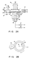
- Figs. 2A and 2B are views for explaining an arrangement of a semiconductor substrate etching apparatus of the present invention.
- Fig. 2A is a front view including a partially sectional view.
- Fig. 2B is a partial plan view of the apparatus.
- a rotary first vacuum chuck 11 includes an elastic seal member 12 (an O-ring is used in this embodiment, and hence the seal member 12 will be referred to as an O-ring hereinafter.)
- Reference numeral 1 denotes a semiconductor substrate (wafer) whose end surface is to be etched.
- the O-ring 12 is constituted by a high-modulus member and has a diameter smaller than that of the substrate 1.
- the O-ring 12 is in tight contact with one major surface (to be referred to as a lower surface hereinafter) 1b of the substrate 1 to hold the substrate 1 in a horizontal state.
- the O-ring 12 is fitted in a notched portion which is formed in the peripheral portion of an upper surface 19 of the first vacuum chuck 11.
- the first vacuum chuck 11 is fixed on a hollow rotating shaft 16.
- a hollow portion 14, as an exhaust path, is formed inside the first vacuum chuck 11 so as to communicate with the hollow portion of the rotating shaft 16.
- Several exhaust holes 15 are formed in the first vacuum chuck 11 so as to communicate with the hollow portion 14 and to obliquely extend outward at an angle of 45 or 60° to be open to the upper surface 19.
- the openings of the exhaust holes 15 are arranged from the center to the periphery in a straight line (see Fig. 2B). In this embodiment, the openings are radially arranged from the center of the upper surface in a straight line.
- the present invention is not limited to this. That is, the above arrangement may be curved or shifted from the radial direction.
- the openings can be arranged in any of the above-described manners as long as they are inclined obliquely outward, as described above.
- the rotating shaft 16 is coupled to a rotational driving unit (not shown).
- the rotational speed of the rotating shaft 16 can be changed, and a rotational driving unit capable of rotating the shaft 16 at a high speed of 2,000 rpm or more as needed is used.
- One end of the hollow portion of the rotating shaft 16 is connected to a vacuum pipe line and an N2 gas pipe line in parallel through valves 17 and 18, respectively.
- An etching mechanism 21 for the end surface of a semiconductor substrate includes a roller 21b fixed on a rotating shaft 22, and an etching solution supply means (etching solution supply nozzle) 23.
- the roller 21b is arranged near the substrate 1 in a horizontal state.
- a groove 21a is formed in the outer surface of the roller 21b.
- the groove 21a is shaped so as to allow the end surface of the substrate 1 to be inserted in a non-contact state, i.e., to cover the end surface of the substrate.
- the etching solution supply means 23 is a nozzle which is arranged near the roller 21b so as to supply an etching solution to the groove 21a of the rotating roller 21b. Note that the etching solution supply means is not limited to the nozzle in this embodiment.
- an etching solution supply path may be formed in the rotating shaft 22 and the roller 21b so as to extend therethrough and to be open to the groove 21a.
- the rotating shaft 22 is coupled to a rotational driving unit (not shown), and transmits rotation of a desired rotation speed to the roller 21b.
- a second vacuum chuck 31 is arranged at an upper position to oppose the first vacuum chuck 11 through the substrate 1, and is coupled to a driving unit (not shown) capable of horizontally and vertically moving the chuck 31.
- This driving unit includes a rotary mechanism, as needed, in order to rotate the second vacuum chuck 31 in cleaning and drying steps for substrates (to be described later).
- An exhaust hole 32 is formed inside the second vacuum chuck 31 so as to communicate with a vacuum pipe line (not shown) and to be open to a suction surface 33.
- An elastic seal member is arranged around the peripheral portion of the suction surface 33 as needed.
- the second vacuum chuck 31 is designed to hold the other major surface (to be referred to as an upper surface hereinafter) of the substrate 1 by suction and to move and stop the substrate to an upper position which is a predetermined distance away from the upper surface 19.
- a semiconductor substrate cleaning mechanism 41 includes an end surface cleaning nozzle 42 and a cleaning nozzle 43.
- the cleaning nozzle 42 is arranged at a position to oppose the side surface of the substrate 1 held by the first vacuum chuck 11 so that a cleaning solution can be sprayed on the end surface including the side surface of the substrate 1.
- the cleaning nozzle 43 is arranged at a position to oppose the side surface of a region defined by the predetermined distance between the upper surface 19 of the first vacuum chuck 11 and the lower surface of the substrate 1 held by the second vacuum chuck 31 by suction. The cleaning nozzle 43 is used to spray a cleaning solution on this region.
- a semiconductor substrate drying mechanism 50 includes the exhaust holes 15 communicating with the hollow portion 14 of the first vacuum chuck 11, the N2 gas pipe line coupled to the rotating shaft 16 through the valve 18, and a rotational driving unit (not shown) which can rotate at high speed and is coupled to the rotating shaft 16.
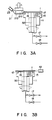
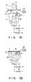
- FIG. 3A the semiconductor substrate 1 is placed on the first vacuum chuck 11.
- the valve 17 is then opened to evacuate the interior of the chuck 11 so as to hold the substrate 1 with a vacuum.
- the respective rotational driving units (not shown) are energized to rotate the first vacuum chuck 11 and the roller 21b in the opposite directions, as shown in Fig. 2B.
- An etching solution supplied from the etching solution supply nozzle 23 is held in the groove 21a of the roller 21b with surface tension.
- the groove 21a is arranged to cover the end surface of the substrate 1, the end surface is brought into contact with the etching solution upon rotation of the roller 21b and of the substrate 1. As a result, the etching solution is transferred onto the end surface, and an etching process of only the end surface is performed.
- a cleaning solution e.g., pure water
- a cleaning solution is sprayed from the end surface cleaning nozzle 42 on the end surface of the rotating substrate 1, thereby cleaning the end surface of the substrate 1 and removing the etching solution therefrom.
- the second vacuum chuck 31 which moves to a position above the first vacuum chuck 11 is lowered to receive the substrate 1 from the first vacuum chuck 11 and hold it by vacuum suction.
- the valve 17 is closed.
- the substrate 1 is held by the second vacuum chuck 31, it is raised and stopped at a position at which the predetermined distance is defined between the lower surface 1b of the substrate 1 and the upper surface 19 of the first vacuum chuck 19.
- the first and second vacuum chucks 11 and 31 are rotated by the rotational driving units (not shown) in the opposite directions.
- the valve 18 for an N2 gas is then opened to discharge the N2 gas outward from the exhaust holes 15, and a cleaning solution is sprayed on the region defined by the predetermined distance using the cleaning nozzle 43.
- the upper surface 19 of the first vacuum chuck 11 and the lower surface 1b of the substrate 1 which rotates in the direction opposite to that of the vacuum chuck 11 are cleaned within a short period of time by the cleaning solution which is sprayed together with the discharged N2 gas. It is apparent that the cleaning solution does not flow into the exhaust holes 15. After cleaning, a drying process is performed by flowing the N2 gas for several seconds.
- valve 18 After drying, the valve 18 is closed to stop the N2 gas.
- the second vacuum chuck 31 is lowered to transfer the substrate 1 on the O-ring 12 of the first vacuum chuck 1, as shown in Fig. 3D.
- the valve 17 is then opened to vacuum-chuck the substrate 1.
- a cleaning solution is sprayed from the cleaning nozzle 43 on the rotating substrate 1 so as to clean the upper surface 1a of the substrate 1.
- the first vacuum chuck 11 is rotated at 3,000 rpm to dry the upper surface 1a.
- the problems of the conventional techniques can be solved, and an etching process can be limited to only the end surface of a substrate, thus automatically performing the etching process within a short period of time.
- cleaning and drying steps after the etching process can be continuously and automatically performed, the manufacturing yield can be increased, the time required for the respective steps can be shortened, the consumption of chemicals can be reduced, and the safety of operations can be improved as compared with the conventional technique.
Applications Claiming Priority (2)
| Application Number | Priority Date | Filing Date | Title |
|---|---|---|---|
| JP63285285A JPH02130922A (ja) | 1988-11-11 | 1988-11-11 | 半導体基板エッチング装置 |
| JP285285/88 | 1988-11-11 |
Publications (3)
| Publication Number | Publication Date |
|---|---|
| EP0368334A2 true EP0368334A2 (de) | 1990-05-16 |
| EP0368334A3 EP0368334A3 (de) | 1991-05-08 |
| EP0368334B1 EP0368334B1 (de) | 1997-03-19 |
Family
ID=17689536
Family Applications (1)
| Application Number | Title | Priority Date | Filing Date |
|---|---|---|---|
| EP89120883A Expired - Lifetime EP0368334B1 (de) | 1988-11-11 | 1989-11-10 | Ätzvorrichtung und Verfahren zu deren Anwendung |
Country Status (5)
| Country | Link |
|---|---|
| US (1) | US4968375A (de) |
| EP (1) | EP0368334B1 (de) |
| JP (1) | JPH02130922A (de) |
| KR (1) | KR920010730B1 (de) |
| DE (1) | DE68927870T2 (de) |
Cited By (9)
| Publication number | Priority date | Publication date | Assignee | Title |
|---|---|---|---|---|
| EP0954389A1 (de) * | 1996-08-29 | 1999-11-10 | Ontrak Systems, Inc. | Gekerbte walze und system mit einer solchen walze |
| WO2000045428A1 (fr) * | 1999-01-28 | 2000-08-03 | Stmicroelectronics S.A. | Dressage du bord d'une plaquette semiconductrice et machine de dressage correspondante |
| EP1037261A2 (de) * | 1999-03-15 | 2000-09-20 | Nec Corporation | Verfahren Zur Ätzung und Reinigung und Vorrichtungen dafür |
| WO2000059029A2 (en) * | 1999-03-31 | 2000-10-05 | Lam Research Corporation | Method and apparatus for enabling conventional wire bonding to copper-based bond pad features |
| EP1136592A2 (de) * | 2000-03-22 | 2001-09-26 | Applied Materials, Inc. | Verfahren und Vorrichtung zum Entfernen von unerwünschten elektroplattierten Ablagerungen |
| WO2003023825A2 (en) * | 2001-09-05 | 2003-03-20 | Ebara Corporation | Substrate processing apparatus |
| US6884303B2 (en) * | 2000-09-29 | 2005-04-26 | International Rectifier Corporation | Process of thinning and blunting semiconductor wafer edge and resulting wafer |
| US7543593B2 (en) | 2001-08-02 | 2009-06-09 | Tokyo Electron Limited | Substrate processing apparatus |
| CN102439698A (zh) * | 2009-05-22 | 2012-05-02 | 大阳日酸株式会社 | 气相生长装置 |
Families Citing this family (52)
| Publication number | Priority date | Publication date | Assignee | Title |
|---|---|---|---|---|
| JPH0810686B2 (ja) * | 1990-09-14 | 1996-01-31 | 株式会社東芝 | 半導体基板エッチング処理装置 |
| JPH0715897B2 (ja) * | 1991-11-20 | 1995-02-22 | 株式会社エンヤシステム | ウエ−ハ端面エッチング方法及び装置 |
| JP2602766B2 (ja) * | 1993-02-18 | 1997-04-23 | エム・セテック株式会社 | ウェハーエッジの加工方法とその装置 |
| JP3388628B2 (ja) * | 1994-03-24 | 2003-03-24 | 東京応化工業株式会社 | 回転式薬液処理装置 |
| TW281795B (de) * | 1994-11-30 | 1996-07-21 | Sharp Kk | |
| US5952050A (en) * | 1996-02-27 | 1999-09-14 | Micron Technology, Inc. | Chemical dispensing system for semiconductor wafer processing |
| JP3641115B2 (ja) * | 1997-10-08 | 2005-04-20 | 大日本スクリーン製造株式会社 | 基板処理装置 |
| US6117778A (en) * | 1998-02-11 | 2000-09-12 | International Business Machines Corporation | Semiconductor wafer edge bead removal method and tool |
| KR20000002998A (ko) * | 1998-06-25 | 2000-01-15 | 윤종용 | 엘씨디 글래스 세정장치 |
| US6202658B1 (en) * | 1998-11-11 | 2001-03-20 | Applied Materials, Inc. | Method and apparatus for cleaning the edge of a thin disc |
| DE19854743A1 (de) * | 1998-11-27 | 2000-06-08 | Sez Semiconduct Equip Zubehoer | Vorrichtung zum Naßätzen einer Kante einer Halbleiterscheibe |
| US6523553B1 (en) * | 1999-03-30 | 2003-02-25 | Applied Materials, Inc. | Wafer edge cleaning method and apparatus |
| JP2000331975A (ja) * | 1999-05-19 | 2000-11-30 | Ebara Corp | ウエハ洗浄装置 |
| KR20010008521A (ko) * | 1999-07-01 | 2001-02-05 | 김영환 | 웨이퍼의 빽엔드 결점제거장치 |
| US6309981B1 (en) * | 1999-10-01 | 2001-10-30 | Novellus Systems, Inc. | Edge bevel removal of copper from silicon wafers |
| US7780867B1 (en) | 1999-10-01 | 2010-08-24 | Novellus Systems, Inc. | Edge bevel removal of copper from silicon wafers |
| US6497241B1 (en) * | 1999-12-23 | 2002-12-24 | Lam Research Corporation | Hollow core spindle and spin, rinse, and dry module including the same |
| US6586342B1 (en) | 2000-04-25 | 2003-07-01 | Novellus Systems, Inc. | Edge bevel removal of copper from silicon wafers |
| US7000622B2 (en) * | 2002-09-30 | 2006-02-21 | Lam Research Corporation | Methods and systems for processing a bevel edge of a substrate using a dynamic liquid meniscus |
| US6805769B2 (en) * | 2000-10-13 | 2004-10-19 | Dainippon Screen Mfg. Co., Ltd. | Substrate processing apparatus |
| KR100436361B1 (ko) * | 2000-12-15 | 2004-06-18 | (주)케이.씨.텍 | 기판 가장자리를 세정하기 위한 장치 |
| US6669808B2 (en) * | 2001-03-22 | 2003-12-30 | Dainippon Screen Mfg. Co., Ltd. | Substrate processing apparatus and substrate processing method |
| AT413162B (de) * | 2001-09-26 | 2005-11-15 | Sez Ag | Ringförmige aufnahmevorrichtung für einen rotierenden träger zur aufnahme eines scheibenförmigen gegenstandes wie eines halbleiterwafers |
| KR100430737B1 (ko) * | 2001-10-08 | 2004-05-10 | 주식회사 실트론 | 웨이퍼의 에지 표면 에칭처리장치 |
| JP2003124180A (ja) * | 2001-10-16 | 2003-04-25 | Ebara Corp | 基板処理装置 |
| JP4018958B2 (ja) * | 2001-10-30 | 2007-12-05 | 大日本スクリーン製造株式会社 | 基板処理装置 |
| US20040132295A1 (en) * | 2002-11-01 | 2004-07-08 | Basol Bulent M. | Method and device to remove unwanted material from the edge region of a workpiece |
| US20040226654A1 (en) * | 2002-12-17 | 2004-11-18 | Akihisa Hongo | Substrate processing apparatus and substrate processing method |
| KR20040110391A (ko) * | 2003-06-19 | 2004-12-31 | 삼성전자주식회사 | 기판 처리 장치 |
| KR100562502B1 (ko) * | 2003-07-02 | 2006-03-21 | 삼성전자주식회사 | 반도체 기판의 가장자리부 처리 장치 및 방법 |
| US7370659B2 (en) * | 2003-08-06 | 2008-05-13 | Micron Technology, Inc. | Photolithographic stepper and/or scanner machines including cleaning devices and methods of cleaning photolithographic stepper and/or scanner machines |
| US7654221B2 (en) * | 2003-10-06 | 2010-02-02 | Applied Materials, Inc. | Apparatus for electroless deposition of metals onto semiconductor substrates |
| US7827930B2 (en) | 2004-01-26 | 2010-11-09 | Applied Materials, Inc. | Apparatus for electroless deposition of metals onto semiconductor substrates |
| US7476290B2 (en) * | 2003-10-30 | 2009-01-13 | Ebara Corporation | Substrate processing apparatus and substrate processing method |
| US7350315B2 (en) | 2003-12-22 | 2008-04-01 | Lam Research Corporation | Edge wheel dry manifold |
| US7089687B2 (en) * | 2004-09-30 | 2006-08-15 | Lam Research Corporation | Wafer edge wheel with drying function |
| JP3933670B2 (ja) * | 2005-03-29 | 2007-06-20 | 東京エレクトロン株式会社 | 基板洗浄方法及び基板洗浄装置 |
| US7583358B2 (en) * | 2005-07-25 | 2009-09-01 | Micron Technology, Inc. | Systems and methods for retrieving residual liquid during immersion lens photolithography |
| US7456928B2 (en) * | 2005-08-29 | 2008-11-25 | Micron Technology, Inc. | Systems and methods for controlling ambient pressure during processing of microfeature workpieces, including during immersion lithography |
| JP2007115728A (ja) * | 2005-10-18 | 2007-05-10 | Sumco Corp | ウェーハの枚葉式エッチング装置及びウェーハの枚葉式エッチング方法 |
| US8472004B2 (en) * | 2006-01-18 | 2013-06-25 | Micron Technology, Inc. | Immersion photolithography scanner |
| US8100081B1 (en) | 2006-06-30 | 2012-01-24 | Novellus Systems, Inc. | Edge removal of films using externally generated plasma species |
| US9732416B1 (en) | 2007-04-18 | 2017-08-15 | Novellus Systems, Inc. | Wafer chuck with aerodynamic design for turbulence reduction |
| US8322300B2 (en) * | 2008-02-07 | 2012-12-04 | Sunpower Corporation | Edge coating apparatus with movable roller applicator for solar cell substrates |
| US8662008B2 (en) * | 2008-02-07 | 2014-03-04 | Sunpower Corporation | Edge coating apparatus for solar cell substrates |
| US8419964B2 (en) | 2008-08-27 | 2013-04-16 | Novellus Systems, Inc. | Apparatus and method for edge bevel removal of copper from silicon wafers |
| US8172646B2 (en) * | 2009-02-27 | 2012-05-08 | Novellus Systems, Inc. | Magnetically actuated chuck for edge bevel removal |
| US20120175343A1 (en) * | 2011-01-12 | 2012-07-12 | Siltronic Corporation | Apparatus and method for etching a wafer edge |
| DE102011103576A1 (de) | 2011-05-30 | 2012-12-06 | Megamotive Gmbh & Co. Kg | Drehwinkelsensor |
| JP6945314B2 (ja) * | 2017-03-24 | 2021-10-06 | 株式会社Screenホールディングス | 基板処理装置 |
| JP7171371B2 (ja) * | 2018-11-01 | 2022-11-15 | 東邦化成株式会社 | エッチング装置 |
| EP4113584A1 (de) * | 2021-07-02 | 2023-01-04 | Semsysco GmbH | System und verfahren zur oberflächenbehandlung eines substrats mit einer flüssigkeit |
Citations (2)
| Publication number | Priority date | Publication date | Assignee | Title |
|---|---|---|---|---|
| US4339297A (en) * | 1981-04-14 | 1982-07-13 | Seiichiro Aigo | Apparatus for etching of oxide film on semiconductor wafer |
| JPS57143831A (en) * | 1981-03-03 | 1982-09-06 | Toshiba Corp | Process of semiconductor wafer |
Family Cites Families (1)
| Publication number | Priority date | Publication date | Assignee | Title |
|---|---|---|---|---|
| DE3027934A1 (de) * | 1980-07-23 | 1982-02-25 | Siemens AG, 1000 Berlin und 8000 München | Verfahren zur einseitigen aetzung von halbleiterscheiben |
-
1988
- 1988-11-11 JP JP63285285A patent/JPH02130922A/ja active Granted
-
1989
- 1989-11-08 US US07/433,165 patent/US4968375A/en not_active Expired - Lifetime
- 1989-11-10 EP EP89120883A patent/EP0368334B1/de not_active Expired - Lifetime
- 1989-11-10 DE DE68927870T patent/DE68927870T2/de not_active Expired - Fee Related
- 1989-11-11 KR KR1019890016354A patent/KR920010730B1/ko not_active IP Right Cessation
Patent Citations (2)
| Publication number | Priority date | Publication date | Assignee | Title |
|---|---|---|---|---|
| JPS57143831A (en) * | 1981-03-03 | 1982-09-06 | Toshiba Corp | Process of semiconductor wafer |
| US4339297A (en) * | 1981-04-14 | 1982-07-13 | Seiichiro Aigo | Apparatus for etching of oxide film on semiconductor wafer |
Non-Patent Citations (1)
| Title |
|---|
| PATENT ABSTRACTS OF JAPAN vol. 6, no. 243 (E-145)(1121) 02 December 1982, & JP-A-57 143831 (TOKYO SHIBAURA) 06 September 1982, * |
Cited By (22)
| Publication number | Priority date | Publication date | Assignee | Title |
|---|---|---|---|---|
| EP0954389A4 (de) * | 1996-08-29 | 2006-07-26 | Lam Res Corp | Gekerbte walze und system mit einer solchen walze |
| EP0954389A1 (de) * | 1996-08-29 | 1999-11-10 | Ontrak Systems, Inc. | Gekerbte walze und system mit einer solchen walze |
| WO2000045428A1 (fr) * | 1999-01-28 | 2000-08-03 | Stmicroelectronics S.A. | Dressage du bord d'une plaquette semiconductrice et machine de dressage correspondante |
| FR2789224A1 (fr) * | 1999-01-28 | 2000-08-04 | St Microelectronics Sa | Dressage de bord d'une plaquette semiconductrice |
| US7862658B2 (en) | 1999-03-15 | 2011-01-04 | Renesas Electronics Corporation | Etching and cleaning methods and etching and cleaning apparatuses used therefor |
| EP1037261A3 (de) * | 1999-03-15 | 2002-11-06 | Nec Corporation | Verfahren Zur Ätzung und Reinigung und Vorrichtungen dafür |
| US8420549B2 (en) | 1999-03-15 | 2013-04-16 | Renesas Electronics Corporation | Etching and cleaning methods and etching and cleaning apparatuses used therefor |
| EP1037261A2 (de) * | 1999-03-15 | 2000-09-20 | Nec Corporation | Verfahren Zur Ätzung und Reinigung und Vorrichtungen dafür |
| US6964724B2 (en) | 1999-03-15 | 2005-11-15 | Nec Corporation | Etching and cleaning methods and etching and cleaning apparatuses used therefor |
| WO2000059029A3 (en) * | 1999-03-31 | 2001-02-15 | Lam Res Corp | Method and apparatus for enabling conventional wire bonding to copper-based bond pad features |
| WO2000059029A2 (en) * | 1999-03-31 | 2000-10-05 | Lam Research Corporation | Method and apparatus for enabling conventional wire bonding to copper-based bond pad features |
| EP1136592A2 (de) * | 2000-03-22 | 2001-09-26 | Applied Materials, Inc. | Verfahren und Vorrichtung zum Entfernen von unerwünschten elektroplattierten Ablagerungen |
| EP1136592A3 (de) * | 2000-03-22 | 2009-03-25 | Applied Materials, Inc. | Verfahren und Vorrichtung zum Entfernen von unerwünschten elektroplattierten Ablagerungen |
| US6884303B2 (en) * | 2000-09-29 | 2005-04-26 | International Rectifier Corporation | Process of thinning and blunting semiconductor wafer edge and resulting wafer |
| US7543593B2 (en) | 2001-08-02 | 2009-06-09 | Tokyo Electron Limited | Substrate processing apparatus |
| US7862680B2 (en) | 2001-08-02 | 2011-01-04 | Tokyo Electron Limited | Substrate processing apparatus |
| US6932884B2 (en) | 2001-09-05 | 2005-08-23 | Ebara Corporation | Substrate processing apparatus |
| WO2003023825A3 (en) * | 2001-09-05 | 2003-11-20 | Ebara Corp | Substrate processing apparatus |
| WO2003023825A2 (en) * | 2001-09-05 | 2003-03-20 | Ebara Corporation | Substrate processing apparatus |
| CN102439698A (zh) * | 2009-05-22 | 2012-05-02 | 大阳日酸株式会社 | 气相生长装置 |
| CN102439698B (zh) * | 2009-05-22 | 2014-10-22 | 大阳日酸株式会社 | 气相生长装置 |
| TWI497570B (zh) * | 2009-05-22 | 2015-08-21 | Taiyo Nippon Sanso Corp | Gas growth device |
Also Published As
| Publication number | Publication date |
|---|---|
| DE68927870D1 (de) | 1997-04-24 |
| US4968375A (en) | 1990-11-06 |
| EP0368334A3 (de) | 1991-05-08 |
| EP0368334B1 (de) | 1997-03-19 |
| KR900008636A (ko) | 1990-06-04 |
| JPH0435901B2 (de) | 1992-06-12 |
| JPH02130922A (ja) | 1990-05-18 |
| KR920010730B1 (ko) | 1992-12-14 |
| DE68927870T2 (de) | 1997-08-07 |
Similar Documents
| Publication | Publication Date | Title |
|---|---|---|
| US4968375A (en) | Etching apparatus | |
| EP0157675B1 (de) | Wirbeleinrichtung zur Behandlung eines Substrates, insbesondere einer Halbleiterscheibe | |
| KR100488378B1 (ko) | 기판 세정 방법 및 기판 세정 장치 | |
| KR100445259B1 (ko) | 세정방법 및 이를 수행하기 위한 세정 장치 | |
| KR100283445B1 (ko) | 도포장치및그방법 | |
| WO2001084621A1 (en) | Rotation holding device and semiconductor substrate processing device | |
| JPH0573245B2 (de) | ||
| KR20080082846A (ko) | 기판 박판화 방법, 기판 박판화 장치 및 이를 포함하는기판 박판화 시스템 | |
| JP2001319908A (ja) | 被処理物のウエット処理方法及びその装置 | |
| JP2001319849A (ja) | 液処理装置及び液処理方法 | |
| JPH10242110A (ja) | 回転処理方法および回転処理装置 | |
| JP3088118B2 (ja) | 板状物処理装置および板状物処理方法ならびに半導体装置の製造方法 | |
| GB2349742A (en) | Method and apparatus for processing a wafer to remove an unnecessary substance therefrom | |
| JPH05253853A (ja) | 薄片吸着装置および薄片吸着装置の洗浄方法 | |
| KR20100060094A (ko) | 기판 이면 세정 방법 | |
| JPH07122529A (ja) | 半導体素子のシール式スピンエッチング装置 | |
| JPH09134872A (ja) | レジスト剥離方法及び装置 | |
| JPH01316936A (ja) | 半導体基板エッチング処理装置 | |
| TWI804897B (zh) | 基板處理方法以及基板處理裝置 | |
| KR200238129Y1 (ko) | 반도체웨이퍼세정장비의웨이퍼뒷면이물제거장치 | |
| KR102139604B1 (ko) | 기판 처리 장치 및 기판 처리 방법 | |
| JP3901777B2 (ja) | 基板洗浄装置のゲート装置 | |
| JP2003001178A (ja) | 基板処理装置および基板処理方法 | |
| JPH05315240A (ja) | 現像装置 | |
| JPH0611024B2 (ja) | 現像方法 |
Legal Events
| Date | Code | Title | Description |
|---|---|---|---|
| PUAI | Public reference made under article 153(3) epc to a published international application that has entered the european phase |
Free format text: ORIGINAL CODE: 0009012 |
|
| 17P | Request for examination filed |
Effective date: 19891110 |
|
| AK | Designated contracting states |
Kind code of ref document: A2 Designated state(s): CH DE FR GB LI |
|
| PUAL | Search report despatched |
Free format text: ORIGINAL CODE: 0009013 |
|
| AK | Designated contracting states |
Kind code of ref document: A3 Designated state(s): CH DE FR GB LI |
|
| 17Q | First examination report despatched |
Effective date: 19920901 |
|
| GRAG | Despatch of communication of intention to grant |
Free format text: ORIGINAL CODE: EPIDOS AGRA |
|
| GRAH | Despatch of communication of intention to grant a patent |
Free format text: ORIGINAL CODE: EPIDOS IGRA |
|
| GRAH | Despatch of communication of intention to grant a patent |
Free format text: ORIGINAL CODE: EPIDOS IGRA |
|
| GRAA | (expected) grant |
Free format text: ORIGINAL CODE: 0009210 |
|
| AK | Designated contracting states |
Kind code of ref document: B1 Designated state(s): CH DE FR GB LI |
|
| REG | Reference to a national code |
Ref country code: CH Ref legal event code: EP |
|
| REF | Corresponds to: |
Ref document number: 68927870 Country of ref document: DE Date of ref document: 19970424 |
|
| ET | Fr: translation filed | ||
| REG | Reference to a national code |
Ref country code: CH Ref legal event code: NV Representative=s name: E. BLUM & CO. PATENTANWAELTE |
|
| PGFP | Annual fee paid to national office [announced via postgrant information from national office to epo] |
Ref country code: FR Payment date: 19971112 Year of fee payment: 9 |
|
| PGFP | Annual fee paid to national office [announced via postgrant information from national office to epo] |
Ref country code: DE Payment date: 19971114 Year of fee payment: 9 |
|
| PLBE | No opposition filed within time limit |
Free format text: ORIGINAL CODE: 0009261 |
|
| STAA | Information on the status of an ep patent application or granted ep patent |
Free format text: STATUS: NO OPPOSITION FILED WITHIN TIME LIMIT |
|
| 26N | No opposition filed | ||
| REG | Reference to a national code |
Ref country code: GB Ref legal event code: 746 Effective date: 19980917 |
|
| PG25 | Lapsed in a contracting state [announced via postgrant information from national office to epo] |
Ref country code: FR Free format text: LAPSE BECAUSE OF NON-PAYMENT OF DUE FEES Effective date: 19990730 |
|
| REG | Reference to a national code |
Ref country code: FR Ref legal event code: ST |
|
| PG25 | Lapsed in a contracting state [announced via postgrant information from national office to epo] |
Ref country code: DE Free format text: LAPSE BECAUSE OF NON-PAYMENT OF DUE FEES Effective date: 19990901 |
|
| REG | Reference to a national code |
Ref country code: GB Ref legal event code: IF02 |
|
| PGFP | Annual fee paid to national office [announced via postgrant information from national office to epo] |
Ref country code: GB Payment date: 20051109 Year of fee payment: 17 |
|
| PGFP | Annual fee paid to national office [announced via postgrant information from national office to epo] |
Ref country code: CH Payment date: 20051115 Year of fee payment: 17 |
|
| PG25 | Lapsed in a contracting state [announced via postgrant information from national office to epo] |
Ref country code: LI Free format text: LAPSE BECAUSE OF NON-PAYMENT OF DUE FEES Effective date: 20061130 Ref country code: CH Free format text: LAPSE BECAUSE OF NON-PAYMENT OF DUE FEES Effective date: 20061130 |
|
| REG | Reference to a national code |
Ref country code: CH Ref legal event code: PL |
|
| GBPC | Gb: european patent ceased through non-payment of renewal fee |
Effective date: 20061110 |
|
| PG25 | Lapsed in a contracting state [announced via postgrant information from national office to epo] |
Ref country code: GB Free format text: LAPSE BECAUSE OF NON-PAYMENT OF DUE FEES Effective date: 20061110 |