EP0361195B1 - Plaque à circuit imprimé avec substrat moulé - Google Patents
Plaque à circuit imprimé avec substrat moulé Download PDFInfo
- Publication number
- EP0361195B1 EP0361195B1 EP89116804A EP89116804A EP0361195B1 EP 0361195 B1 EP0361195 B1 EP 0361195B1 EP 89116804 A EP89116804 A EP 89116804A EP 89116804 A EP89116804 A EP 89116804A EP 0361195 B1 EP0361195 B1 EP 0361195B1
- Authority
- EP
- European Patent Office
- Prior art keywords
- depressions
- substrate
- circuit board
- printed circuit
- trench
- Prior art date
- Legal status (The legal status is an assumption and is not a legal conclusion. Google has not performed a legal analysis and makes no representation as to the accuracy of the status listed.)
- Expired - Lifetime
Links
Images

Classifications
-
- H—ELECTRICITY
- H05—ELECTRIC TECHNIQUES NOT OTHERWISE PROVIDED FOR
- H05K—PRINTED CIRCUITS; CASINGS OR CONSTRUCTIONAL DETAILS OF ELECTRIC APPARATUS; MANUFACTURE OF ASSEMBLAGES OF ELECTRICAL COMPONENTS
- H05K1/00—Printed circuits
- H05K1/02—Details
- H05K1/11—Printed elements for providing electric connections to or between printed circuits
- H05K1/115—Via connections; Lands around holes or via connections
- H05K1/116—Lands, clearance holes or other lay-out details concerning the surrounding of a via
-
- H—ELECTRICITY
- H05—ELECTRIC TECHNIQUES NOT OTHERWISE PROVIDED FOR
- H05K—PRINTED CIRCUITS; CASINGS OR CONSTRUCTIONAL DETAILS OF ELECTRIC APPARATUS; MANUFACTURE OF ASSEMBLAGES OF ELECTRICAL COMPONENTS
- H05K1/00—Printed circuits
-
- H—ELECTRICITY
- H05—ELECTRIC TECHNIQUES NOT OTHERWISE PROVIDED FOR
- H05K—PRINTED CIRCUITS; CASINGS OR CONSTRUCTIONAL DETAILS OF ELECTRIC APPARATUS; MANUFACTURE OF ASSEMBLAGES OF ELECTRICAL COMPONENTS
- H05K3/00—Apparatus or processes for manufacturing printed circuits
- H05K3/10—Apparatus or processes for manufacturing printed circuits in which conductive material is applied to the insulating support in such a manner as to form the desired conductive pattern
- H05K3/107—Apparatus or processes for manufacturing printed circuits in which conductive material is applied to the insulating support in such a manner as to form the desired conductive pattern by filling grooves in the support with conductive material
-
- H—ELECTRICITY
- H05—ELECTRIC TECHNIQUES NOT OTHERWISE PROVIDED FOR
- H05K—PRINTED CIRCUITS; CASINGS OR CONSTRUCTIONAL DETAILS OF ELECTRIC APPARATUS; MANUFACTURE OF ASSEMBLAGES OF ELECTRICAL COMPONENTS
- H05K2201/00—Indexing scheme relating to printed circuits covered by H05K1/00
- H05K2201/03—Conductive materials
- H05K2201/0332—Structure of the conductor
- H05K2201/0364—Conductor shape
- H05K2201/0376—Flush conductors, i.e. flush with the surface of the printed circuit
-
- H—ELECTRICITY
- H05—ELECTRIC TECHNIQUES NOT OTHERWISE PROVIDED FOR
- H05K—PRINTED CIRCUITS; CASINGS OR CONSTRUCTIONAL DETAILS OF ELECTRIC APPARATUS; MANUFACTURE OF ASSEMBLAGES OF ELECTRICAL COMPONENTS
- H05K2201/00—Indexing scheme relating to printed circuits covered by H05K1/00
- H05K2201/09—Shape and layout
- H05K2201/09009—Substrate related
- H05K2201/09036—Recesses or grooves in insulating substrate
-
- H—ELECTRICITY
- H05—ELECTRIC TECHNIQUES NOT OTHERWISE PROVIDED FOR
- H05K—PRINTED CIRCUITS; CASINGS OR CONSTRUCTIONAL DETAILS OF ELECTRIC APPARATUS; MANUFACTURE OF ASSEMBLAGES OF ELECTRICAL COMPONENTS
- H05K2201/00—Indexing scheme relating to printed circuits covered by H05K1/00
- H05K2201/09—Shape and layout
- H05K2201/09009—Substrate related
- H05K2201/09118—Moulded substrate
-
- H—ELECTRICITY
- H05—ELECTRIC TECHNIQUES NOT OTHERWISE PROVIDED FOR
- H05K—PRINTED CIRCUITS; CASINGS OR CONSTRUCTIONAL DETAILS OF ELECTRIC APPARATUS; MANUFACTURE OF ASSEMBLAGES OF ELECTRICAL COMPONENTS
- H05K2201/00—Indexing scheme relating to printed circuits covered by H05K1/00
- H05K2201/09—Shape and layout
- H05K2201/09818—Shape or layout details not covered by a single group of H05K2201/09009 - H05K2201/09809
- H05K2201/09827—Tapered, e.g. tapered hole, via or groove
-
- H—ELECTRICITY
- H05—ELECTRIC TECHNIQUES NOT OTHERWISE PROVIDED FOR
- H05K—PRINTED CIRCUITS; CASINGS OR CONSTRUCTIONAL DETAILS OF ELECTRIC APPARATUS; MANUFACTURE OF ASSEMBLAGES OF ELECTRICAL COMPONENTS
- H05K2201/00—Indexing scheme relating to printed circuits covered by H05K1/00
- H05K2201/09—Shape and layout
- H05K2201/09818—Shape or layout details not covered by a single group of H05K2201/09009 - H05K2201/09809
- H05K2201/09845—Stepped hole, via, edge, bump or conductor
-
- H—ELECTRICITY
- H05—ELECTRIC TECHNIQUES NOT OTHERWISE PROVIDED FOR
- H05K—PRINTED CIRCUITS; CASINGS OR CONSTRUCTIONAL DETAILS OF ELECTRIC APPARATUS; MANUFACTURE OF ASSEMBLAGES OF ELECTRICAL COMPONENTS
- H05K2201/00—Indexing scheme relating to printed circuits covered by H05K1/00
- H05K2201/09—Shape and layout
- H05K2201/09818—Shape or layout details not covered by a single group of H05K2201/09009 - H05K2201/09809
- H05K2201/09981—Metallised walls
-
- H—ELECTRICITY
- H05—ELECTRIC TECHNIQUES NOT OTHERWISE PROVIDED FOR
- H05K—PRINTED CIRCUITS; CASINGS OR CONSTRUCTIONAL DETAILS OF ELECTRIC APPARATUS; MANUFACTURE OF ASSEMBLAGES OF ELECTRICAL COMPONENTS
- H05K2203/00—Indexing scheme relating to apparatus or processes for manufacturing printed circuits covered by H05K3/00
- H05K2203/05—Patterning and lithography; Masks; Details of resist
- H05K2203/0562—Details of resist
- H05K2203/0574—Stacked resist layers used for different processes
-
- H—ELECTRICITY
- H05—ELECTRIC TECHNIQUES NOT OTHERWISE PROVIDED FOR
- H05K—PRINTED CIRCUITS; CASINGS OR CONSTRUCTIONAL DETAILS OF ELECTRIC APPARATUS; MANUFACTURE OF ASSEMBLAGES OF ELECTRICAL COMPONENTS
- H05K2203/00—Indexing scheme relating to apparatus or processes for manufacturing printed circuits covered by H05K3/00
- H05K2203/14—Related to the order of processing steps
- H05K2203/1415—Applying catalyst after applying plating resist
-
- H—ELECTRICITY
- H05—ELECTRIC TECHNIQUES NOT OTHERWISE PROVIDED FOR
- H05K—PRINTED CIRCUITS; CASINGS OR CONSTRUCTIONAL DETAILS OF ELECTRIC APPARATUS; MANUFACTURE OF ASSEMBLAGES OF ELECTRICAL COMPONENTS
- H05K3/00—Apparatus or processes for manufacturing printed circuits
- H05K3/10—Apparatus or processes for manufacturing printed circuits in which conductive material is applied to the insulating support in such a manner as to form the desired conductive pattern
- H05K3/18—Apparatus or processes for manufacturing printed circuits in which conductive material is applied to the insulating support in such a manner as to form the desired conductive pattern using precipitation techniques to apply the conductive material
- H05K3/181—Apparatus or processes for manufacturing printed circuits in which conductive material is applied to the insulating support in such a manner as to form the desired conductive pattern using precipitation techniques to apply the conductive material by electroless plating
- H05K3/182—Apparatus or processes for manufacturing printed circuits in which conductive material is applied to the insulating support in such a manner as to form the desired conductive pattern using precipitation techniques to apply the conductive material by electroless plating characterised by the patterning method
- H05K3/184—Apparatus or processes for manufacturing printed circuits in which conductive material is applied to the insulating support in such a manner as to form the desired conductive pattern using precipitation techniques to apply the conductive material by electroless plating characterised by the patterning method using masks
-
- H—ELECTRICITY
- H05—ELECTRIC TECHNIQUES NOT OTHERWISE PROVIDED FOR
- H05K—PRINTED CIRCUITS; CASINGS OR CONSTRUCTIONAL DETAILS OF ELECTRIC APPARATUS; MANUFACTURE OF ASSEMBLAGES OF ELECTRICAL COMPONENTS
- H05K3/00—Apparatus or processes for manufacturing printed circuits
- H05K3/30—Assembling printed circuits with electric components, e.g. with resistor
- H05K3/32—Assembling printed circuits with electric components, e.g. with resistor electrically connecting electric components or wires to printed circuits
- H05K3/34—Assembling printed circuits with electric components, e.g. with resistor electrically connecting electric components or wires to printed circuits by soldering
- H05K3/3452—Solder masks
-
- H—ELECTRICITY
- H05—ELECTRIC TECHNIQUES NOT OTHERWISE PROVIDED FOR
- H05K—PRINTED CIRCUITS; CASINGS OR CONSTRUCTIONAL DETAILS OF ELECTRIC APPARATUS; MANUFACTURE OF ASSEMBLAGES OF ELECTRICAL COMPONENTS
- H05K3/00—Apparatus or processes for manufacturing printed circuits
- H05K3/40—Forming printed elements for providing electric connections to or between printed circuits
- H05K3/42—Plated through-holes or plated via connections
- H05K3/425—Plated through-holes or plated via connections characterised by the sequence of steps for plating the through-holes or via connections in relation to the conductive pattern
- H05K3/426—Plated through-holes or plated via connections characterised by the sequence of steps for plating the through-holes or via connections in relation to the conductive pattern initial plating of through-holes in substrates without metal
-
- Y—GENERAL TAGGING OF NEW TECHNOLOGICAL DEVELOPMENTS; GENERAL TAGGING OF CROSS-SECTIONAL TECHNOLOGIES SPANNING OVER SEVERAL SECTIONS OF THE IPC; TECHNICAL SUBJECTS COVERED BY FORMER USPC CROSS-REFERENCE ART COLLECTIONS [XRACs] AND DIGESTS
- Y10—TECHNICAL SUBJECTS COVERED BY FORMER USPC
- Y10T—TECHNICAL SUBJECTS COVERED BY FORMER US CLASSIFICATION
- Y10T29/00—Metal working
- Y10T29/49—Method of mechanical manufacture
- Y10T29/49002—Electrical device making
- Y10T29/49117—Conductor or circuit manufacturing
- Y10T29/49124—On flat or curved insulated base, e.g., printed circuit, etc.
- Y10T29/49155—Manufacturing circuit on or in base
- Y10T29/49158—Manufacturing circuit on or in base with molding of insulated base
- Y10T29/4916—Simultaneous circuit manufacturing
-
- Y—GENERAL TAGGING OF NEW TECHNOLOGICAL DEVELOPMENTS; GENERAL TAGGING OF CROSS-SECTIONAL TECHNOLOGIES SPANNING OVER SEVERAL SECTIONS OF THE IPC; TECHNICAL SUBJECTS COVERED BY FORMER USPC CROSS-REFERENCE ART COLLECTIONS [XRACs] AND DIGESTS
- Y10—TECHNICAL SUBJECTS COVERED BY FORMER USPC
- Y10T—TECHNICAL SUBJECTS COVERED BY FORMER US CLASSIFICATION
- Y10T29/00—Metal working
- Y10T29/49—Method of mechanical manufacture
- Y10T29/49002—Electrical device making
- Y10T29/49117—Conductor or circuit manufacturing
- Y10T29/49124—On flat or curved insulated base, e.g., printed circuit, etc.
- Y10T29/49155—Manufacturing circuit on or in base
- Y10T29/49165—Manufacturing circuit on or in base by forming conductive walled aperture in base
Definitions
- the invention relates to a printed circuit board with an injection molded substrate, in the surface of which the circuit pattern is recessed by trench-shaped depressions in the area of conductor tracks and by flat depressions in the area of plated-through holes and / or connection areas and the recessed areas have a conductive metal coating.
- Such printed circuit boards with injection molded or similarly shaped substrates are already known from DE-A-27 15 875 or the corresponding CA-A-10 75 825 or also from US-A-45 32 152.
- the substrate is first formed in a form in which the conductor pattern and via holes are contained in the form of depressions. After a mechanical and / or chemical surface treatment, the substrate is then chemically activated, whereupon the raised surfaces of the substrate are covered with a protective layer. When this protective layer is applied, only the depressions have to be left free, so that complex photostructuring of the resist can be dispensed with and the application can be carried out, for example, with a doctor blade or by roller coating, the so-called roller coating.
- a conductive metal coating is then preferably applied by electroless metal deposition, which leads to the formation of the entire conductor configuration in the depressions of the substrate and in the via holes.
- a solder resist is applied to the conductor surfaces that are not to be soldered.
- the structuring of the substrate before the metal deposition does not result in photostructuring of the resist is required.
- the application of the solder resist then requires either selective application to the conductor tracks or photo structuring, since the flat depressions which surround the plated-through holes as soldering eyes or which are to serve as connecting surfaces must remain free.
- the invention has for its object to provide a printed circuit board with an injection molded substrate, in which the application of the solder resist can be carried out in a simple manner without photo structuring.
- the invention is based on the knowledge that, due to a geometry of the substrate with correspondingly narrow trench-shaped depressions when electroless or electroless and galvanic deposition of the metal coating, these depressions grow from the bottom and from the side walls until the trench-shaped depression is completely filled. When this complete filling of the trench-shaped depressions is achieved, there is a metal coating in the correspondingly large flat depressions, the thickness of which does not extend to the surface of the substrate and the thickness of which does not fill the flat depressions in the lateral wall area.
- the metal coating is preferably formed by chemically applied copper, which, as already mentioned, is then coated with a suitable solder layer, in particular tin, in the area of soldering eyes, soldering pads and through-holes.
- the trench-shaped depressions (30) have an approximately V-shaped cross section. Such a V-shaped cross section then favors the filling of the trench-shaped depressions in the electroless or electroless and galvanic metal deposition.
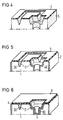
- FIG. 1 shows a section through part of a substrate 1, for example made of glass fiber-reinforced polyetherimide.
- a substrate 1 for example made of glass fiber-reinforced polyetherimide.
- substantially V-shaped trench-shaped depressions 30 of width b, and sheet-like depressions 40 of width B arranged in the region of via holes 60, are already in the injection molding process and in other places sheet-like depressions 50 of the same width B are produced.
- a metal coating 2 the trench-shaped depressions 30 are completely filled with metal up to the surface 10 of the substrate. This is achieved by a correspondingly narrow dimensioning of the width b of the trench-shaped depressions 30, which leads to the growth of the depression 30 during the metal deposition on the bottom and on the side walls of the depression.
- the metal coating 2 is thus deposited flatly and with a small thickness, so that a distance from the surface 10 of the substrate 1, denoted by A, remains here. This means that even with the same depths of the trench-shaped depressions 30 on the one hand and the flat depressions 40 and 50 on the other hand, a metal deposition carried out in the same bath once extends to the surface 10 of the substrate and ends at a distance A from the surface of the substrate 10.
- the distance A must then be so large in any case that when the surface 10 is coated with a solder resist, only the conductor tracks in the area of the trench-shaped depressions 30 but in no way the soldering eyes in the area of the flat depressions 40 and the connection areas in the area of the flat depressions 50 to be covered.
- a solder resist which cannot be seen from FIG. 1, the regions of the metal layer 2 serving as vias, soldering pads and connection surfaces can be coated with a tin layer 3 by hot tinning.
- a substrate 1 is assumed, which according to the example is an injection molded part FIG. 2 contains the approximately V-shaped trench-shaped depressions 30 corresponding to the conductor pattern, the flat depressions 40 and the vias 60 emanating therefrom.
- a surface layer 4 which is a conventional plating resist, is then applied to the surface 10 of this substrate 1 after a conventional surface treatment according to FIG. 3.
- the lacquer layer 4 is applied by roller coating, the depressions 30 and 40 remaining free.
- germination 5 is subsequently applied, which is indicated in the drawing by fine dots. This germination 5 is applied, for example, by immersing the substrate 1 in a PdCl2-SnCl2 bath.
- the metal layer 2 is then applied to the areas not protected by a lacquer layer 4 by chemical metal deposition without external current. It can be seen that this metal layer 2 applied in a commercially available electroless copper bath has reached a thickness by corresponding dimensioning of the coating duration, which corresponds to a complete filling of the trench-shaped depressions 30 to the substrate surface.
- a solder resist 6 is then applied by roller coating, which leaves the flat depressions 40 and the plated-through holes 60 free as a result of the distance A shown in FIG. 1 and here enables the tin layer 3 to be applied by hot tinning. It can be seen that the lacquer layer 4 does not have to be removed before the solder resist 6 is applied.
Landscapes
- Engineering & Computer Science (AREA)
- Microelectronics & Electronic Packaging (AREA)
- Manufacturing & Machinery (AREA)
- Manufacturing Of Printed Wiring (AREA)
- Injection Moulding Of Plastics Or The Like (AREA)
- Parts Printed On Printed Circuit Boards (AREA)
- Structure Of Printed Boards (AREA)
Claims (4)
- Plaquette à circuits imprimés comportant un substrat (1) moulé par injection, sur la surface (10) duquel la configuration des conducteurs est évidée grâce à la présence de renforcements en forme de sillons (3) situés dans la zone de voies conductrices et par des renfoncements d'une certaine étendue (40,50) situés dans la zone de contacts traversants et/ou de surfaces de raccordement et les zones évidées possèdent un revêtement métallique conducteur (2), caractérisée par le fait que la largeur (b) des renfoncements en forme de sillons (30) est choisie suffisamment étroite et la largeur (b) des renfoncements d'une certaine étendue (40,50) est choisie suffisamment large pour que le revêtement métallique déposé (2) remplisse les renfoncements en forme de sillons (30) jusqu'à la surface (10) du substrat (1) et qu'une distance (A) subsiste entre le revêtement métallique (2) situé dans le renfoncement d'une certaine étendue (40,50) et la surface (10) du substrat (1).
- Plaquette à circuits imprimés suivant la revendication 1, caractérisée par le fait que le revêtement métallique (2) est recouvert par une couche d'étain (3) déposée par étamage à chaud, dans la zone des renfoncements d'une certaine étendue (40,50).
- Plaquette à circuits imprimés suivant la revendication 1 ou 2, caractérisée par le fait que le revêtement métallique (2) est formé par du cuivre déposé chimiquement.
- Plaquette à circuits imprimés suivant l'une des revendications précédentes, caractérisée par le fait que les renfoncements en forme de sillons (30) possèdent une section transversale approximativement en forme de V.
Applications Claiming Priority (2)
| Application Number | Priority Date | Filing Date | Title |
|---|---|---|---|
| DE3833297 | 1988-09-30 | ||
| DE3833297 | 1988-09-30 |
Publications (3)
| Publication Number | Publication Date |
|---|---|
| EP0361195A2 EP0361195A2 (fr) | 1990-04-04 |
| EP0361195A3 EP0361195A3 (en) | 1990-08-22 |
| EP0361195B1 true EP0361195B1 (fr) | 1993-03-17 |
Family
ID=6364105
Family Applications (1)
| Application Number | Title | Priority Date | Filing Date |
|---|---|---|---|
| EP89116804A Expired - Lifetime EP0361195B1 (fr) | 1988-09-30 | 1989-09-11 | Plaque à circuit imprimé avec substrat moulé |
Country Status (4)
| Country | Link |
|---|---|
| US (1) | US4985600A (fr) |
| EP (1) | EP0361195B1 (fr) |
| JP (1) | JPH02143487A (fr) |
| DE (1) | DE58903799D1 (fr) |
Cited By (2)
| Publication number | Priority date | Publication date | Assignee | Title |
|---|---|---|---|---|
| CN102131346B (zh) * | 2010-01-15 | 2014-08-06 | 欣兴电子股份有限公司 | 线路板及其制作方法 |
| CN109041433A (zh) * | 2018-09-26 | 2018-12-18 | 生益电子股份有限公司 | 一种槽底过孔阻焊塞孔的制作方法及pcb |
Families Citing this family (23)
| Publication number | Priority date | Publication date | Assignee | Title |
|---|---|---|---|---|
| US5055637A (en) * | 1989-05-02 | 1991-10-08 | Hagner George R | Circuit boards with recessed traces |
| JP2502902B2 (ja) * | 1992-12-28 | 1996-05-29 | インターナショナル・ビジネス・マシーンズ・コーポレイション | プリント配線板およびその製造方法 |
| US5536908A (en) * | 1993-01-05 | 1996-07-16 | Schlumberger Technology Corporation | Lead-free printed circuit assembly |
| US5455741A (en) * | 1993-10-26 | 1995-10-03 | Pulse Engineering, Inc. | Wire-lead through hole interconnect device |
| US5462622A (en) * | 1994-06-09 | 1995-10-31 | Illinois Tool Works Inc. | Molding an electrical element within a premold element and an overmold element to provide a one-piece component |
| US6005463A (en) * | 1997-01-30 | 1999-12-21 | Pulse Engineering | Through-hole interconnect device with isolated wire-leads and component barriers |
| US5796050A (en) * | 1997-02-05 | 1998-08-18 | International Business Machines Corporation | Flexible board having adhesive in surface channels |
| US5994648A (en) * | 1997-03-27 | 1999-11-30 | Ford Motor Company | Three-dimensional molded sockets for mechanical and electrical component attachment |
| US6444489B1 (en) | 2000-12-15 | 2002-09-03 | Charles W. C. Lin | Semiconductor chip assembly with bumped molded substrate |
| US7564409B2 (en) * | 2001-03-26 | 2009-07-21 | Ertek Inc. | Antennas and electrical connections of electrical devices |
| US6582887B2 (en) | 2001-03-26 | 2003-06-24 | Daniel Luch | Electrically conductive patterns, antennas and methods of manufacture |
| US7394425B2 (en) * | 2001-03-26 | 2008-07-01 | Daniel Luch | Electrically conductive patterns, antennas and methods of manufacture |
| US7452656B2 (en) | 2001-03-26 | 2008-11-18 | Ertek Inc. | Electrically conductive patterns, antennas and methods of manufacture |
| US6486549B1 (en) | 2001-11-10 | 2002-11-26 | Bridge Semiconductor Corporation | Semiconductor module with encapsulant base |
| US20050067675A1 (en) * | 2003-08-19 | 2005-03-31 | Shepard Daniel Robert | Molded substrate for topograpy based lithography |
| CN102131336B (zh) * | 2010-01-15 | 2012-08-29 | 欣兴电子股份有限公司 | 线路板及其制程 |
| TWI417013B (zh) * | 2010-05-14 | 2013-11-21 | Kuang Hong Prec Co Ltd | 立體電路元件及其製作方法 |
| TWI417014B (zh) * | 2011-03-23 | 2013-11-21 | Unimicron Technology Corp | 線路板的內埋式線路結構的製造方法 |
| KR20140083580A (ko) * | 2012-12-26 | 2014-07-04 | 삼성전기주식회사 | 인쇄회로기판 및 그 제조방법 |
| US11272621B2 (en) * | 2012-12-28 | 2022-03-08 | Shenzhen Royole Technologies Co., Ltd. | Substrate and method for fabricating flexible electronic device and rigid substrate |
| JP6165640B2 (ja) * | 2014-01-10 | 2017-07-19 | 株式会社東芝 | 配線基板およびその製造方法 |
| TWI590735B (zh) * | 2014-12-15 | 2017-07-01 | 財團法人工業技術研究院 | 訊號傳輸板及其製作方法 |
| JP2019175968A (ja) * | 2018-03-28 | 2019-10-10 | 富士通株式会社 | 回路基板及び回路基板の製造方法 |
Family Cites Families (9)
| Publication number | Priority date | Publication date | Assignee | Title |
|---|---|---|---|---|
| CA1075825A (fr) * | 1976-04-22 | 1980-04-15 | Rollin W. Mettler | Plaquette de circuit et methode de fabrication |
| US4363930A (en) * | 1980-02-04 | 1982-12-14 | Amp Incorporated | Circuit path conductors in plural planes |
| DE3010610A1 (de) * | 1980-03-20 | 1981-10-01 | Schoeller & Co Elektronik Gmbh, 3552 Wetter | Verfahren zur selektiven verzinnung der loetaugen von gedruckten schaltungen |
| DE3014041C2 (de) * | 1980-04-11 | 1982-04-08 | Braun Ag, 6000 Frankfurt | Verfahren zur Aufbringung von elektrisch leitenden Bahnen auf einen Träger aus Isolierstoff |
| US4374457A (en) * | 1980-08-04 | 1983-02-22 | Wiech Raymond E Jr | Method of fabricating complex micro-circuit boards and substrates |
| EP0051378A2 (fr) * | 1980-11-03 | 1982-05-12 | AMP INCORPORATED (a New Jersey corporation) | Plaquette à circuit moulé et procédé de fabrication |
| US4532152A (en) * | 1982-03-05 | 1985-07-30 | Elarde Vito D | Fabrication of a printed circuit board with metal-filled channels |
| US4604799A (en) * | 1982-09-03 | 1986-08-12 | John Fluke Mfg. Co., Inc. | Method of making molded circuit board |
| US4510347A (en) * | 1982-12-06 | 1985-04-09 | Fine Particles Technology Corporation | Formation of narrow conductive paths on a substrate |
-
1989
- 1989-09-11 EP EP89116804A patent/EP0361195B1/fr not_active Expired - Lifetime
- 1989-09-11 DE DE8989116804T patent/DE58903799D1/de not_active Expired - Fee Related
- 1989-09-13 US US07/406,551 patent/US4985600A/en not_active Expired - Fee Related
- 1989-09-28 JP JP1256920A patent/JPH02143487A/ja active Pending
Cited By (3)
| Publication number | Priority date | Publication date | Assignee | Title |
|---|---|---|---|---|
| CN102131346B (zh) * | 2010-01-15 | 2014-08-06 | 欣兴电子股份有限公司 | 线路板及其制作方法 |
| CN109041433A (zh) * | 2018-09-26 | 2018-12-18 | 生益电子股份有限公司 | 一种槽底过孔阻焊塞孔的制作方法及pcb |
| CN109041433B (zh) * | 2018-09-26 | 2020-10-16 | 生益电子股份有限公司 | 一种槽底过孔阻焊塞孔的制作方法及pcb |
Also Published As
| Publication number | Publication date |
|---|---|
| US4985600A (en) | 1991-01-15 |
| EP0361195A2 (fr) | 1990-04-04 |
| DE58903799D1 (de) | 1993-04-22 |
| EP0361195A3 (en) | 1990-08-22 |
| JPH02143487A (ja) | 1990-06-01 |
Similar Documents
| Publication | Publication Date | Title |
|---|---|---|
| EP0361195B1 (fr) | Plaque à circuit imprimé avec substrat moulé | |
| EP0361193B1 (fr) | Plaque de circuit à substrat moulé par injection | |
| EP0361192B1 (fr) | Procédé de fabrication de plaques de circuit | |
| DE69937153T2 (de) | Gedruckte leiterplatte und verfahren zu deren herstellung | |
| DE2817950A1 (de) | Elektrischer schalter | |
| DE1057672B (de) | Verfahren zur Herstellung eingelegter Stromkreise | |
| DE3502744C2 (fr) | ||
| DE3839891C2 (de) | Verfahren zum Herstellen von Lötschichten auf elektronischen Chip-Bauteilen | |
| DE3700912C2 (fr) | ||
| CH543218A (de) | Verfahren zum Herstellen einer gedruckten Schaltung auf einem Metallkern | |
| DE4131065A1 (de) | Verfahren zur herstellung von leiterplatten | |
| DE1142926B (de) | Verfahren zur Herstellung gedruckter Schaltungsplatten | |
| EP0757885B1 (fr) | Procede de formation de motifs conducteurs metalliques sur des substrats electriquement isolants | |
| DE3006117C2 (de) | Verfahren zum Herstellen von Leiterplatten mit mindestens zwei Leiterzugebenen | |
| DE1665395B1 (de) | Verfahren zur herstellung gedruckter leiterplatten | |
| EP0370133A1 (fr) | Procédé de fabrication d'un circuit imprimé | |
| DE102009023629B4 (de) | Leiterplatte und Herstellungsverfahren | |
| DE1615853A1 (de) | Verfahren zum Herstellen von gedruckten Schaltungen | |
| DE3523646A1 (de) | Mehrschichtige schaltungsplatine mit plattierten durchgangsbohrungen | |
| EP0278485B1 (fr) | Méthode de fabrication d'une plaquette utilisable pour la digitalisation | |
| EP0530564A1 (fr) | Procédé pour la fabrication d'un panneau de circuit | |
| DE1811377A1 (de) | Verfahren zur Herstellung gedruckter Leiterplatten | |
| DE2114075A1 (de) | Trockenelektrolytkondensator und Verfahren zu seiner Herstellung | |
| EP0144413A1 (fr) | Carte imprimee pour le montage en surface de circuits integres miniature et procede de fabrication de telles cartes imprimees | |
| DE2013258C3 (de) | Verfahren zur Herstellung von stiftförmigen Anschlußteilen einer gedruckten Schaltungsplatte |
Legal Events
| Date | Code | Title | Description |
|---|---|---|---|
| PUAI | Public reference made under article 153(3) epc to a published international application that has entered the european phase |
Free format text: ORIGINAL CODE: 0009012 |
|
| AK | Designated contracting states |
Kind code of ref document: A2 Designated state(s): DE FR GB IT |
|
| PUAL | Search report despatched |
Free format text: ORIGINAL CODE: 0009013 |
|
| AK | Designated contracting states |
Kind code of ref document: A3 Designated state(s): DE FR GB IT |
|
| 17P | Request for examination filed |
Effective date: 19900904 |
|
| 17Q | First examination report despatched |
Effective date: 19920724 |
|
| GRAA | (expected) grant |
Free format text: ORIGINAL CODE: 0009210 |
|
| AK | Designated contracting states |
Kind code of ref document: B1 Designated state(s): DE FR GB IT |
|
| PG25 | Lapsed in a contracting state [announced via postgrant information from national office to epo] |
Ref country code: IT Free format text: LAPSE BECAUSE OF FAILURE TO SUBMIT A TRANSLATION OF THE DESCRIPTION OR TO PAY THE FEE WITHIN THE PRE;WARNING: LAPSES OF ITALIAN PATENTS WITH EFFECTIVE DATE BEFORE 2007 MAY HAVE OCCURRED AT ANY TIME BEFORE 2007. THE CORRECT EFFECTIVE DATE MAY BE DIFFERENT FROM THE ONE RECORDED.SCRIBED TIME-LIMIT Effective date: 19930317 Ref country code: FR Free format text: THE PATENT HAS BEEN ANNULLED BY A DECISION OF A NATIONAL AUTHORITY Effective date: 19930317 |
|
| RIN1 | Information on inventor provided before grant (corrected) |
Inventor name: HEERMAN, MARCEL |
|
| REF | Corresponds to: |
Ref document number: 58903799 Country of ref document: DE Date of ref document: 19930422 |
|
| ET | Fr: translation filed | ||
| GBT | Gb: translation of ep patent filed (gb section 77(6)(a)/1977) |
Effective date: 19930519 |
|
| PG25 | Lapsed in a contracting state [announced via postgrant information from national office to epo] |
Ref country code: GB Effective date: 19930911 |
|
| PLBE | No opposition filed within time limit |
Free format text: ORIGINAL CODE: 0009261 |
|
| STAA | Information on the status of an ep patent application or granted ep patent |
Free format text: STATUS: NO OPPOSITION FILED WITHIN TIME LIMIT |
|
| 26N | No opposition filed | ||
| GBPC | Gb: european patent ceased through non-payment of renewal fee |
Effective date: 19930911 |
|
| PG25 | Lapsed in a contracting state [announced via postgrant information from national office to epo] |
Ref country code: DE Effective date: 19940601 |
|
| REG | Reference to a national code |
Ref country code: FR Ref legal event code: ST |