EP0357084B1 - Apparat zur Korrektur des Dunkelsignals eines Bildsensors - Google Patents
Apparat zur Korrektur des Dunkelsignals eines Bildsensors Download PDFInfo
- Publication number
- EP0357084B1 EP0357084B1 EP89116203A EP89116203A EP0357084B1 EP 0357084 B1 EP0357084 B1 EP 0357084B1 EP 89116203 A EP89116203 A EP 89116203A EP 89116203 A EP89116203 A EP 89116203A EP 0357084 B1 EP0357084 B1 EP 0357084B1
- Authority
- EP
- European Patent Office
- Prior art keywords
- image sensor
- converter
- data
- digital values
- memory
- Prior art date
- Legal status (The legal status is an assumption and is not a legal conclusion. Google has not performed a legal analysis and makes no representation as to the accuracy of the status listed.)
- Expired - Lifetime
Links
Images

Classifications
-
- G—PHYSICS
- G06—COMPUTING OR CALCULATING; COUNTING
- G06F—ELECTRIC DIGITAL DATA PROCESSING
- G06F7/00—Methods or arrangements for processing data by operating upon the order or content of the data handled
- G06F7/38—Methods or arrangements for performing computations using exclusively denominational number representation, e.g. using binary, ternary, decimal representation
- G06F7/48—Methods or arrangements for performing computations using exclusively denominational number representation, e.g. using binary, ternary, decimal representation using non-contact-making devices, e.g. tube, solid state device; using unspecified devices
- G06F7/499—Denomination or exception handling, e.g. rounding or overflow
- G06F7/49942—Significance control
- G06F7/49947—Rounding
-
- H—ELECTRICITY
- H04—ELECTRIC COMMUNICATION TECHNIQUE
- H04N—PICTORIAL COMMUNICATION, e.g. TELEVISION
- H04N25/00—Circuitry of solid-state image sensors [SSIS]; Control thereof
- H04N25/60—Noise processing, e.g. detecting, correcting, reducing or removing noise
- H04N25/63—Noise processing, e.g. detecting, correcting, reducing or removing noise applied to dark current
-
- H—ELECTRICITY
- H04—ELECTRIC COMMUNICATION TECHNIQUE
- H04N—PICTORIAL COMMUNICATION, e.g. TELEVISION
- H04N25/00—Circuitry of solid-state image sensors [SSIS]; Control thereof
- H04N25/70—SSIS architectures; Circuits associated therewith
- H04N25/701—Line sensors
Definitions
- This invention relates to an apparatus for correcting a dark signal of an image sensor which corrects dark signals from an image sensor such as a linear sensor comprising a CCD (Charge Coupled Device), an MOS (Metal Oxide Semiconductor), etc. and outputs exact reading signals.
- an image sensor such as a linear sensor comprising a CCD (Charge Coupled Device), an MOS (Metal Oxide Semiconductor), etc. and outputs exact reading signals.
- the signals outputted in the dark are extremely low in level. Therefore, the sampling is conducted for plural times before the A/D conversion, and the digital values are averaged to enhance the precision of the dark signal data.
- the precision of subtractable values remains to be ⁇ 1/2 LSB (Least Significant Bit) at the most. Due to this matter, the shadowed portion in the images that are reproduced with the corrected signals might be formed with linear blurs.
- This invention was conceived to eliminate such inconveniences encountered in the prior art and aims at providing an apparatus for correcting dark signal of the image sensor which can improve correcting precision for the dark signal by a simple structure and yet without the necessity to increase the resolution of the A/D converter and prevent linear blurs in the shadowed portion of the reproduced images.
- an apparatus for correcting dark signal of image sensor which comprises: an A/D converter which converts output signals from the image sensor into digital values, an adder which adds the digital values in dark for each pixel, a memory which stores the data from the adder on the result of the addition, a random number generating means which generates a random number which is a mean of the stored data in the memory, and a subtracter which subtracts the random number from the digital values at a time of reading of the images and outputs image data.
- the outputs from an image sensor are sampled in the dark in a condition that input light is cut off for plural times and converted from analog signal to digital values.
- the mean of the digital values is obtained as a random number, which is subtracted from the image data for output.
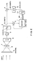
- FIG. 1 shows the principle and construction of this invention wherein the outputs CD from an image sensor in the dark are sampled by an A/D converter 2 and the sampled values are converted into digital values DS of n bits.
- the digital values DS are added by an adder 3 for plural times ( m times) consecutively, and data for each pixel are stored in a memory 1.
- the data MS of N bits (N > n) read out from the memory 1 are inputted to a random number generator 10.
- the data MS which have been stored in the memory 1 are then passed through the random number generator 10 which disperses the least significant bit LSB of the read out data PS at a propability shown by a data bit section which is less than the number of bits of the real data.
- the corrected data RD ( n bits) outputted from the random number generator 10 is subtracted by a subtracter 4 from the digital values DS from the A/D converter 2 at the time of reading the images of the image sensor, and the result is outputted as the read-out and corrected data PS. Since the least significant bit of the corrected data RD from the random number generator 10 is outputted at random in either "1" or "0" due to generation of the random number, the corrected values of the least significant bit would not be fixed but averaged for the least significant bit of the data PS.
- FIG.2 shows an embodiment of this invention wherein an original 5 such as a mounted film is illuminated with the light from a light source. and the light transmitted through the original 5 is inputted to an image sensor 8 such as a linear sensor comprising, for instance, a CCD, via a shutter 6 and a lens 7.
- the analog signal output from the image sensor 8 is amplified by an amplifier 9 into read-out signals CD (0 - 2 V) and inputted to an A/D (analog to digital) converter 2.
- the digital values DS (8 bits) converted by the A/D converter 2 are added for plural times by an adder 3, for instance, for 256 times, and the result of the addition is inputted and stored in a memory 1.
- the read-out digital data MS (16 bits) from the memory 1 are converted by a D/A converter 11 into analog signals AS of 0 - 2 V and inputted to an A/D converter 12 of 8 bits while the digital values RD (8 bits) which have been converted by the A/D converter 12 are inputted to a subtracter 4 as data for correction.
- the D/A converter 11 and the A/D converter 12 form a means to generate random numbers.
- the shutter 6 is provided between the lens 7 and the original 5 so that either the dark signal data or the image signals of the original 5 may be obtained by opening/closing the shutter 6.
- the dark signal from the image sensor 8 are converted by the A/D converter 2 into digital values for each pixel, and are added at the adder 3 through the memory 1 by sampling for 256 times, and the result of addition is stored in the memory 1.
- the outputs from the image sensor 8 are converted from analog to digital values by the A/D converter 2, and the digital values DS are inputted to the subtracter 4.
- the data MS stores in the memory 1 are read out from the memory 1 in response to pixel clocks, and the read-out data MS are converted into analog signals AS by the D/A converter 11.
- the analog signals AS are further converted into digital values by the A/D converter 12 of 8 bits, and the data RD for the correction are subtracted from the digital values DS of the images signals by the subtracter 4, to be outputted as the corrected and read-out data PS.
- the means to generate random numbers is constructed with a D/A converter 11 and an A/D converter 12 in the embodiment shown in FlG.2, the entire construction may be in digital.
- the correcting apparatus can realize dark signal correction for the image sensor at a high precision with a relatively simple structure and can prevent linear blurs which may otherwise occurring in the shadowed portion reproduced images.
Landscapes
- Engineering & Computer Science (AREA)
- Multimedia (AREA)
- Signal Processing (AREA)
- General Physics & Mathematics (AREA)
- Physics & Mathematics (AREA)
- Theoretical Computer Science (AREA)
- Computational Mathematics (AREA)
- Computing Systems (AREA)
- Mathematical Analysis (AREA)
- Mathematical Optimization (AREA)
- Pure & Applied Mathematics (AREA)
- General Engineering & Computer Science (AREA)
- Transforming Light Signals Into Electric Signals (AREA)
- Facsimile Image Signal Circuits (AREA)
- Picture Signal Circuits (AREA)
Claims (5)
- Ein Apparat zum Korrigieren eines Dunkelsignals eines Bildsensors, wobei der Apparat umfaßt: einen ersten A/D-Konverter (2), welcher Ausgangssignale aus dem Bildsensor in Digitalwerte umwandelt, einen Addierer (3), welcher die Digitalwerte im Dunkeln für jedes Pixel addiert, einen Speicher (1), welcher die Daten aus dem Addierer im Ergebnis der Addition speichert, eine Zufallszahlerzeugungseinrichtung (10), welche eine Zufallszahl derart erzeugt, daß sie ein Mittel der gespeicherten Daten in dem Speicher ist, und eine Subtraktionseinrichtung (4), welche die Zufallszahl von den Digitalwerten zu einer Zeit während des Lesens des Bildes subtrahiert und Bilddaten ausgibt.
- Ein Apparat nach Anspruch 1, wobei der Bildsensor eine CCD-Einrichtung umfaßt.
- Ein Apparat nach Anspruch 2, wobei der Bildsensor ein Linearsensor ist.
- Ein Apparat nach Anspruch 1, wobei die Zufallszahlerzeugungseinrichtung einen D/A-Konverter (11) umfaßt, welcher Ausgangsdaten des Speichers aufnimmt, einen zweiten A/D-Konverter (12), welcher ein aus dem D/A-Konverter (11) ausgegebenes Analogsignal aufnimmt und das Mittel der gespeicherten Daten ausgibt.
- Ein Apparat nach Anspruch 4, wobei die Digitalwerte aus dem ersten A/D-Konverter (2) 8-Bit-Werte sind, die Addition durch den Addierer (3) 256mal wiederholt wird und die Ausgangsdaten des Speichers (1) 16-Bit-Daten sind.
Applications Claiming Priority (2)
| Application Number | Priority Date | Filing Date | Title |
|---|---|---|---|
| JP63219724A JP2587470B2 (ja) | 1988-09-02 | 1988-09-02 | イメージセンサの暗時出力補正装置 |
| JP219724/88 | 1988-09-02 |
Publications (2)
| Publication Number | Publication Date |
|---|---|
| EP0357084A1 EP0357084A1 (de) | 1990-03-07 |
| EP0357084B1 true EP0357084B1 (de) | 1993-04-21 |
Family
ID=16739975
Family Applications (1)
| Application Number | Title | Priority Date | Filing Date |
|---|---|---|---|
| EP89116203A Expired - Lifetime EP0357084B1 (de) | 1988-09-02 | 1989-09-01 | Apparat zur Korrektur des Dunkelsignals eines Bildsensors |
Country Status (3)
| Country | Link |
|---|---|
| EP (1) | EP0357084B1 (de) |
| JP (1) | JP2587470B2 (de) |
| DE (1) | DE68906100T2 (de) |
Families Citing this family (12)
| Publication number | Priority date | Publication date | Assignee | Title |
|---|---|---|---|---|
| WO1991007844A1 (en) * | 1989-11-15 | 1991-05-30 | Rank Cintel Limited | Improvements in and relating to flying spot scanners |
| US5086343A (en) * | 1990-05-11 | 1992-02-04 | Eastman Kodak Company | Method and apparatus for compensating for sensitivity variations in the output of a solid state image sensor |
| DE4117020C2 (de) * | 1990-05-25 | 1993-12-02 | Asahi Optical Co Ltd | Steuervorrichtung für einen Bildsensor |
| JP2802962B2 (ja) * | 1990-05-25 | 1998-09-24 | 旭光学工業株式会社 | 撮像素子駆動装置 |
| EP0673149A1 (de) * | 1994-03-15 | 1995-09-20 | Bayer Corporation | Verfahren und Vorrichtung zur Korrektur der Nichtgleichheit des Dunkelsignals eines Bildsensors |
| US6330371B1 (en) * | 1998-10-19 | 2001-12-11 | Raytheon Company | Adaptive non-uniformity compensation using feedforward shunting and min-mean filter |
| US7084912B2 (en) * | 2001-09-20 | 2006-08-01 | Yuen-Shung Chieh | Method for reducing coherent row-wise and column-wise fixed pattern noise in CMOS image sensors |
| JP3963008B2 (ja) * | 2001-12-20 | 2007-08-22 | 本田技研工業株式会社 | イメージセンサの出力補正装置 |
| JP2008011284A (ja) * | 2006-06-30 | 2008-01-17 | Fujitsu Ltd | 画像処理回路、撮像回路および電子機器 |
| JP4396757B2 (ja) * | 2007-10-22 | 2010-01-13 | ソニー株式会社 | ノイズ補正回路、撮像装置及びノイズ補正方法 |
| CN104270581B (zh) * | 2014-09-29 | 2017-06-06 | 南京大学 | 一种便携式真随机码发生装置及方法 |
| JP6814531B2 (ja) * | 2015-07-29 | 2021-01-20 | シャープ株式会社 | 収納庫 |
Family Cites Families (5)
| Publication number | Priority date | Publication date | Assignee | Title |
|---|---|---|---|---|
| JPS5738071A (en) * | 1980-08-19 | 1982-03-02 | Fuji Photo Film Co Ltd | Output compensation device |
| JPS59154880A (ja) * | 1983-02-24 | 1984-09-03 | Asahi Optical Co Ltd | 光電出力のダ−ク電流補償回路 |
| JPS59194257A (ja) * | 1983-04-18 | 1984-11-05 | Toshiba Corp | デ−タ加工方式 |
| JPS60189372A (ja) * | 1984-03-08 | 1985-09-26 | Dainippon Screen Mfg Co Ltd | 画像入力装置 |
| JP2602217B2 (ja) * | 1987-01-07 | 1997-04-23 | キヤノン株式会社 | 撮像装置 |
-
1988
- 1988-09-02 JP JP63219724A patent/JP2587470B2/ja not_active Expired - Lifetime
-
1989
- 1989-09-01 DE DE8989116203T patent/DE68906100T2/de not_active Expired - Fee Related
- 1989-09-01 EP EP89116203A patent/EP0357084B1/de not_active Expired - Lifetime
Also Published As
| Publication number | Publication date |
|---|---|
| JP2587470B2 (ja) | 1997-03-05 |
| DE68906100D1 (de) | 1993-05-27 |
| JPH0267881A (ja) | 1990-03-07 |
| DE68906100T2 (de) | 1993-07-29 |
| EP0357084A1 (de) | 1990-03-07 |
Similar Documents
| Publication | Publication Date | Title |
|---|---|---|
| EP1252760B1 (de) | Verfahren und gerät zur vorstufensignalverarbeitung für einen bildsensor | |
| EP0357084B1 (de) | Apparat zur Korrektur des Dunkelsignals eines Bildsensors | |
| US5278658A (en) | Image reading apparatus having a function for correcting dark signals generated in a photoelectric conversion element | |
| JPH0247914B2 (de) | ||
| US6914627B1 (en) | Method and apparatus for digital column fixed pattern noise canceling for a CMOS image sensor | |
| US5355164A (en) | Method and apparatus of correction image read signals by removing the influence of dark current therefrom | |
| EP2538659B1 (de) | Bildaufnahmegerät | |
| US7359099B2 (en) | Image reading device and image forming apparatus | |
| JPS6339142B2 (de) | ||
| EP0684731A1 (de) | Rauschunterdrückungsschaltung für Videosignal | |
| JPS6114702B2 (de) | ||
| JPH03195177A (ja) | 画像読取装置 | |
| US4812667A (en) | Past record correcting/reading apparatus | |
| JPH0374967A (ja) | 画像補正回路 | |
| JP2578605B2 (ja) | 高感度化撮像装置 | |
| JP3186230B2 (ja) | 固体撮像素子の欠陥補正装置及び固体撮像装置 | |
| JP3245213B2 (ja) | 画像読取装置 | |
| JPS6161559A (ja) | 情報読取装置 | |
| JP3678318B2 (ja) | 画像読取装置 | |
| JP2004208026A (ja) | 固体撮像装置 | |
| JPH0779345A (ja) | イメージセンサ出力補正回路 | |
| JPH0496582A (ja) | 画像入力装置 | |
| JPS59181877A (ja) | 画像信号安定化方式 | |
| JPS61287376A (ja) | 光電変換素子の安電流補正回路 | |
| JPH0937107A (ja) | 撮像信号補正装置 |
Legal Events
| Date | Code | Title | Description |
|---|---|---|---|
| PUAI | Public reference made under article 153(3) epc to a published international application that has entered the european phase |
Free format text: ORIGINAL CODE: 0009012 |
|
| AK | Designated contracting states |
Kind code of ref document: A1 Designated state(s): DE FR GB |
|
| 17P | Request for examination filed |
Effective date: 19900410 |
|
| 17Q | First examination report despatched |
Effective date: 19920626 |
|
| GRAA | (expected) grant |
Free format text: ORIGINAL CODE: 0009210 |
|
| AK | Designated contracting states |
Kind code of ref document: B1 Designated state(s): DE FR GB |
|
| REF | Corresponds to: |
Ref document number: 68906100 Country of ref document: DE Date of ref document: 19930527 |
|
| ET | Fr: translation filed | ||
| PLBE | No opposition filed within time limit |
Free format text: ORIGINAL CODE: 0009261 |
|
| STAA | Information on the status of an ep patent application or granted ep patent |
Free format text: STATUS: NO OPPOSITION FILED WITHIN TIME LIMIT |
|
| 26N | No opposition filed | ||
| REG | Reference to a national code |
Ref country code: GB Ref legal event code: IF02 |
|
| PGFP | Annual fee paid to national office [announced via postgrant information from national office to epo] |
Ref country code: GB Payment date: 20040827 Year of fee payment: 16 Ref country code: FR Payment date: 20040827 Year of fee payment: 16 |
|
| PGFP | Annual fee paid to national office [announced via postgrant information from national office to epo] |
Ref country code: DE Payment date: 20041027 Year of fee payment: 16 |
|
| PG25 | Lapsed in a contracting state [announced via postgrant information from national office to epo] |
Ref country code: GB Free format text: LAPSE BECAUSE OF NON-PAYMENT OF DUE FEES Effective date: 20050901 |
|
| PG25 | Lapsed in a contracting state [announced via postgrant information from national office to epo] |
Ref country code: DE Free format text: LAPSE BECAUSE OF NON-PAYMENT OF DUE FEES Effective date: 20060401 |
|
| GBPC | Gb: european patent ceased through non-payment of renewal fee |
Effective date: 20050901 |
|
| PG25 | Lapsed in a contracting state [announced via postgrant information from national office to epo] |
Ref country code: FR Free format text: LAPSE BECAUSE OF NON-PAYMENT OF DUE FEES Effective date: 20060531 |
|
| REG | Reference to a national code |
Ref country code: FR Ref legal event code: ST Effective date: 20060531 |
|
| REG | Reference to a national code |
Ref country code: GB Ref legal event code: 732E |