EP0351820A2 - Circuit de sortie - Google Patents
Circuit de sortie Download PDFInfo
- Publication number
- EP0351820A2 EP0351820A2 EP89113244A EP89113244A EP0351820A2 EP 0351820 A2 EP0351820 A2 EP 0351820A2 EP 89113244 A EP89113244 A EP 89113244A EP 89113244 A EP89113244 A EP 89113244A EP 0351820 A2 EP0351820 A2 EP 0351820A2
- Authority
- EP
- European Patent Office
- Prior art keywords
- transistor
- mos transistor
- gate
- control signal
- output
- Prior art date
- Legal status (The legal status is an assumption and is not a legal conclusion. Google has not performed a legal analysis and makes no representation as to the accuracy of the status listed.)
- Granted
Links
Images
Classifications
-
- H—ELECTRICITY
- H03—ELECTRONIC CIRCUITRY
- H03K—PULSE TECHNIQUE
- H03K5/00—Manipulating of pulses not covered by one of the other main groups of this subclass
- H03K5/01—Shaping pulses
- H03K5/02—Shaping pulses by amplifying
-
- H—ELECTRICITY
- H03—ELECTRONIC CIRCUITRY
- H03K—PULSE TECHNIQUE
- H03K19/00—Logic circuits, i.e. having at least two inputs acting on one output; Inverting circuits
- H03K19/02—Logic circuits, i.e. having at least two inputs acting on one output; Inverting circuits using specified components
- H03K19/08—Logic circuits, i.e. having at least two inputs acting on one output; Inverting circuits using specified components using semiconductor devices
- H03K19/094—Logic circuits, i.e. having at least two inputs acting on one output; Inverting circuits using specified components using semiconductor devices using field-effect transistors
- H03K19/0944—Logic circuits, i.e. having at least two inputs acting on one output; Inverting circuits using specified components using semiconductor devices using field-effect transistors using MOSFET or insulated gate field-effect transistors, i.e. IGFET
- H03K19/09448—Logic circuits, i.e. having at least two inputs acting on one output; Inverting circuits using specified components using semiconductor devices using field-effect transistors using MOSFET or insulated gate field-effect transistors, i.e. IGFET in combination with bipolar transistors [BIMOS]
-
- H—ELECTRICITY
- H03—ELECTRONIC CIRCUITRY
- H03K—PULSE TECHNIQUE
- H03K19/00—Logic circuits, i.e. having at least two inputs acting on one output; Inverting circuits
- H03K19/0008—Arrangements for reducing power consumption
- H03K19/0013—Arrangements for reducing power consumption in field effect transistor circuits
-
- H—ELECTRICITY
- H03—ELECTRONIC CIRCUITRY
- H03K—PULSE TECHNIQUE
- H03K19/00—Logic circuits, i.e. having at least two inputs acting on one output; Inverting circuits
- H03K19/01—Modifications for accelerating switching
- H03K19/017—Modifications for accelerating switching in field-effect transistor circuits
- H03K19/01707—Modifications for accelerating switching in field-effect transistor circuits in asynchronous circuits
- H03K19/01721—Modifications for accelerating switching in field-effect transistor circuits in asynchronous circuits by means of a pull-up or down element
-
- H—ELECTRICITY
- H03—ELECTRONIC CIRCUITRY
- H03K—PULSE TECHNIQUE
- H03K5/00—Manipulating of pulses not covered by one of the other main groups of this subclass
- H03K5/13—Arrangements having a single output and transforming input signals into pulses delivered at desired time intervals
- H03K5/133—Arrangements having a single output and transforming input signals into pulses delivered at desired time intervals using a chain of active delay devices
- H03K5/134—Arrangements having a single output and transforming input signals into pulses delivered at desired time intervals using a chain of active delay devices with field-effect transistors
Definitions
- the present invention relates to a high breakdown voltage output circuit for shifting a level of a low-voltage output signal to output a high-voltage output signal.
- CMOS circuit is used to receive an input signal to output a low-voltage signal, and a high-voltage signal obtained by shifting the level of the low-voltage signal is output from a push-pull output stage.
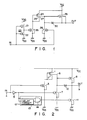
- Fig. 1 is a circuit diagram showing a conventional output circuit used for the above-mentioned drive IC.
- a CMOS inverter 23 is inserted between a low-voltage power supply V DD and a ground voltage V SS .
- the gates and drains of a p-channel MOS transistor 21 and an n-channel MOS transistor 22 are commonly connected to each other.
- the emitter of a high breakdown voltage pnp transistor 24 is connected to a high-voltage power source V CC .
- the transistor 24 has a multicollector structure.
- a first collector 25 is connected to the base of the transistor 24.
- the base of the pnp transistor 24 is connected to the drain of an n-channel DMOS (double diffused MOS) transistor 26, the gate of which is connected to a common drain of the CMOS inverter 23, and the source of which is connected to the ground voltage V SS .
- a second collector 27 of the pnp transistor 24 is connected to the drain of an output pull-down n-channel DMOS transistor 28, the gate of which is connected to a common gate of the CMOS inverter 23, and the source of which is connected to the ground voltage V SS .
- the gate of an output pull-up n-channel DMOS transistor 29 is connected to the second collector 27.
- the drain of the transistor 29 is connected to the high-voltage power source V CC , and a cathode-anode path of a Zener diode 30 is connected to a source-drain path of the transistor 29.
- An input signal In is supplied from the common gate of the CMOS inverter 23, and an output signal Out is output from the source of the n-channel DMOS transistor 29 through an output terminal.
- the transistor 21 in the CMOS inverter 23 is turned off, and the transistor 22 is turned on. Therefore, the transistor 26 is turned off.
- the transistor 28 is turned on in response to the input signal In set at “H” level. As a result, the transistor 29 is turned off, and the output Out goes to "L” level.
- the high-voltage power supply V CC is used in the circuit shown in Fig. 1. Therefore, even if a slight current flows, power consumption is high. In order to minimize the power consumption, an operation current of the level shift transistor 24 must be decreased. Conventionally, an ON current of the transistor 26 has been decreased to solve the above problem. However, the MOS transistor 26 and the transistor 24 constitute a current mirror circuit. Therefore, when the ON current of the MOS transistor 26 is decreased, a current supplied to the collector of the transistor 24 is also decreased. During a pull-up operation of the output, a predetermined voltage drop occurs across the Zener diode 30 in response to a current supplied to the collector 27 of the transistor 24.
- the element sizes of the MOS transistors 28 and 29 are set to be large to realize a sufficiently high load drive capability in order to pull-up or -down the output. Therefore, the value of the parasitic capacitance C is also large. For this reason, a long signal propagation time is present between the input and output operations, and a high-speed operation cannot be achieved in the conventional circuit.
- an output circuit comprising a first MOS transistor, a drain-source path of which is inserted between a first potential and an output terminal, a level shift transistor inserted between the first potential and the gate of a first MOS transistor, a second MOS transistor, a drain-source path of which is inserted between a control terminal of the level shift transistor and a second potential, and the gate of which receives a first control signal, a constant voltage element inserted between the gate of the first MOS transistor and the output terminal, a third MOS transistor, a drain-source path of which is inserted between the output terminal and the second potential through the constant voltage element, and the gate of which receives a second control signal having a phase opposite to that of the first control signal, a signal delay circuit for delaying the second control signal for a predetermined period of time to output a third control signal, and a fourth MOS transistor, a drain-source path of which is inserted between the output terminal and the second potential
- the third MOS transistor connected to the collector of the level shift transistor has a small parasitic capacitance, a delay time when the gate potential of the output pull-up first MOS transistor is increased is reduced. Therefore, even if a limited current is supplied to achieve low power consumption during an output pull-up operation, a delay can be minimized.
- a signal delay circuit is arranged in the output pull-down fourth MOS transistor to delay its gate signal, so that a current flow through the first and fourth MOS transistors can be prevented.
- Fig. 2 is a circuit diagram showing an arrangement of an output circuit according to an embodiment of the present invention.
- the emitter of a high breakdown voltage pnp multicollector transistor 1 is connected to a high-voltage power source V CC .
- a first collector 2 of the transistor 1 is connected to its base.
- the base of the transistor 1 is connected to the drain of an n-channel DMOS transistor 3.
- the gate of the transistor 3 is connected to an input terminal 4 for receiving an input signal In.
- the source of the transistor 3 is connected to a ground voltage V SS .
- the input terminal of an inverter 5 operated by a low-voltage power source VDD is connected to the input terminal 4.
- a second collector 6 of the transistor 1 is connected to the drain of an n-channel DMOS transistor 7.
- the gate of the transistor 7 is connected to an output terminal of the inverter 5.
- the source of the transistor 7 is connected to the ground voltage V SS .
- the drain of an n-channel DMOS transistor 8 is connected to the high-voltage power source V CC .
- the gate of the transistor 8 is connected to the second collector 6 of the transistor 1.
- the source of the transistor 8 is connected to an output terminal 9 for outputting an output signal Out.
- a Zener diode 10 having polarities shown in Fig. 2 is connected between the gate of the transistor 8 and the output terminal 9.
- the drain of an n-channel DMOS transistor 11 is connected to the output terminal 9.
- the source of the transistor 11 is connected to the ground voltage V SS .
- the signal delay controller 12 includes a delay circuit 13 for delaying an output signal from the inverter 5 for a predetermined period of time, and an AND gate 14 for receiving output signals from the delay circuit 13 and the inverter 5.
- the output terminal of the signal delay controller 12 is connected to the gate of the transistor 11. Note that the element size, e.g., the channel width, of the transistor 7 is set to be sufficiently smaller than those of the transistors 8 and 11. The conductance of the transistor 7 is sufficiently smaller than those of the transistors 8 and 11.
- the element size of the transistor 7 is set to be sufficiently smaller than that of the transistor 11, and the value of a parasitic capacitance present in the node of the gate of the transistor 8 is also sufficiently small when viewed from the collector 6 of the transistor 1. For this reason, when the value of an ON current of the transistor 1 is set to be equal to the conventional value, the parasitic capacitance in the node of the gate of the transistor 8 is charged at a higher speed than that in the conventional case upon setting the output signal Out at V CC level.
- the transistor 11 is turned on, and the parasitic capacitance of the output terminal 9 is discharged to the ground voltage V SS through the transistors 7 and 11.
- the output signal Out is set at ground voltage V SS level.
- the value of the parasitic capacitance connected to the node of the gate of the transistor 8 is smaller than that of the conventional circuit. Therefore, when an ON current of the transistor 1 is substantially equal to that of the conventional circuit, a signal delay time can be reduced, as compared with that of the conventional circuit. Since the transistor 11 discharges the parasitic capacitance of the output terminal 9 at high speed, its conductance must be increased to some extent. However, a timing at which a control signal is supplied to the gate of the transistor 11 is delayed with respect to a timing at which the input signal In is supplied. For this reason, a current flowing between the high-voltage power source V CC and the ground voltage V SS through the transistors 8 and 11 is not present. Therefore, even if the transistor 11 is arranged, power consumption is not increased.
- a high breakdown voltage bipolar transistor is used as a level shift circuit in the circuit of this embodiment, a high breakdown voltage MOS field effect transistor can be used.
- the circuit which generates a signal for controlling such an output circuit is not limited to a specific one, and an arrangement of the delay signal controller is not limited.
Landscapes
- Engineering & Computer Science (AREA)
- Physics & Mathematics (AREA)
- Computer Hardware Design (AREA)
- Computing Systems (AREA)
- General Engineering & Computer Science (AREA)
- Mathematical Physics (AREA)
- Power Engineering (AREA)
- Nonlinear Science (AREA)
- Logic Circuits (AREA)
- Electronic Switches (AREA)
- Manipulation Of Pulses (AREA)
Applications Claiming Priority (2)
| Application Number | Priority Date | Filing Date | Title |
|---|---|---|---|
| JP63179682A JPH0229115A (ja) | 1988-07-19 | 1988-07-19 | 出力回路 |
| JP179682/88 | 1988-07-19 |
Publications (3)
| Publication Number | Publication Date |
|---|---|
| EP0351820A2 true EP0351820A2 (fr) | 1990-01-24 |
| EP0351820A3 EP0351820A3 (en) | 1990-05-30 |
| EP0351820B1 EP0351820B1 (fr) | 1994-05-18 |
Family
ID=16070029
Family Applications (1)
| Application Number | Title | Priority Date | Filing Date |
|---|---|---|---|
| EP89113244A Expired - Lifetime EP0351820B1 (fr) | 1988-07-19 | 1989-07-19 | Circuit de sortie |
Country Status (5)
| Country | Link |
|---|---|
| US (1) | US4996449A (fr) |
| EP (1) | EP0351820B1 (fr) |
| JP (1) | JPH0229115A (fr) |
| KR (1) | KR920005354B1 (fr) |
| DE (1) | DE68915351T2 (fr) |
Cited By (10)
| Publication number | Priority date | Publication date | Assignee | Title |
|---|---|---|---|---|
| EP0537970A2 (fr) * | 1991-10-14 | 1993-04-21 | Sharp Kabushiki Kaisha | Circuit de sortie avec tampon |
| EP0545362A1 (fr) * | 1991-12-06 | 1993-06-09 | National Semiconductor Corporation | Circuit de réduction de bruit pour tampon de sortie BICMOS |
| WO1994029798A1 (fr) * | 1993-06-08 | 1994-12-22 | National Semiconductor Corporation | Bus cmos programmable et etage d'attaque pour lignes de transmission |
| US5438282A (en) * | 1993-06-08 | 1995-08-01 | National Semiconductor Corporation | CMOS BTL compatible bus and transmission line driver |
| US5483184A (en) * | 1993-06-08 | 1996-01-09 | National Semiconductor Corporation | Programmable CMOS bus and transmission line receiver |
| US5539341A (en) * | 1993-06-08 | 1996-07-23 | National Semiconductor Corporation | CMOS bus and transmission line driver having programmable edge rate control |
| US5543746A (en) * | 1993-06-08 | 1996-08-06 | National Semiconductor Corp. | Programmable CMOS current source having positive temperature coefficient |
| US5557223A (en) * | 1993-06-08 | 1996-09-17 | National Semiconductor Corporation | CMOS bus and transmission line driver having compensated edge rate control |
| US5818260A (en) * | 1996-04-24 | 1998-10-06 | National Semiconductor Corporation | Transmission line driver having controllable rise and fall times with variable output low and minimal on/off delay |
| EP0880124A1 (fr) * | 1997-05-22 | 1998-11-25 | STMicroelectronics S.A. | Etage de sortie de puissance pour la commande de cellules d'écran à plasma |
Families Citing this family (6)
| Publication number | Priority date | Publication date | Assignee | Title |
|---|---|---|---|---|
| US5015889A (en) * | 1989-02-23 | 1991-05-14 | Reay Robert L | Schottky enhanced CMOS output circuit |
| US5258665A (en) * | 1992-05-12 | 1993-11-02 | National Semiconductor Corporation | AC Miller-Killer circuit for L→Z transitions |
| US5811990A (en) | 1993-10-15 | 1998-09-22 | Micron Technology, Inc. | Voltage pump and a level translator circuit |
| JP2000307406A (ja) * | 1999-04-22 | 2000-11-02 | Denso Corp | 負荷駆動回路 |
| FR2849536B1 (fr) * | 2002-12-27 | 2007-02-23 | St Microelectronics Sa | Circuit d'interface de fourniture de tension |
| JP6424674B2 (ja) * | 2015-02-25 | 2018-11-21 | 日本電気硝子株式会社 | ガラスフィルムの割断方法 |
Citations (5)
| Publication number | Priority date | Publication date | Assignee | Title |
|---|---|---|---|---|
| EP0031907A2 (fr) * | 1980-01-08 | 1981-07-15 | International Business Machines Corporation | Générateur de tension d'entretien pour un panneau à décharge dans un gaz |
| EP0238358A2 (fr) * | 1986-03-20 | 1987-09-23 | Kabushiki Kaisha Toshiba | Circuit tampon |
| EP0239762A2 (fr) * | 1986-03-31 | 1987-10-07 | Kabushiki Kaisha Toshiba | Circuit tampon |
| EP0264614A1 (fr) * | 1986-09-11 | 1988-04-27 | Matsushita Electric Industrial Co., Ltd. | Circuit d'attaque MOSFET fournissant protection contre la rupture dûe aux tensions transitoires |
| EP0372087A1 (fr) * | 1988-05-16 | 1990-06-13 | Kabushiki Kaisha Toshiba | Circuit de commande |
Family Cites Families (10)
| Publication number | Priority date | Publication date | Assignee | Title |
|---|---|---|---|---|
| US4339676A (en) * | 1979-08-13 | 1982-07-13 | Texas Instruments Incorporated | Logic circuit having a selectable output mode |
| US4425517A (en) * | 1981-03-31 | 1984-01-10 | Rca Corporation | Fail soft tri-state logic circuit |
| US4347447A (en) * | 1981-04-16 | 1982-08-31 | Mostek Corporation | Current limiting MOS transistor driver circuit |
| JPS57181231A (en) * | 1981-05-01 | 1982-11-08 | Oki Electric Ind Co Ltd | Semiconductor integrated circuit |
| JPS60198620A (ja) * | 1984-03-21 | 1985-10-08 | Sharp Corp | Lsi化したタイミング発生回路 |
| US4612466A (en) * | 1984-08-31 | 1986-09-16 | Rca Corporation | High-speed output driver |
| US4638187A (en) * | 1985-10-01 | 1987-01-20 | Vtc Incorporated | CMOS output buffer providing high drive current with minimum output signal distortion |
| IT1204808B (it) * | 1986-02-18 | 1989-03-10 | Sgs Microelettronica Spa | Circuito di reset all'accensione per reti logiche in tecnologia mos,particolarmente per periferiche di microprocessori |
| JPS63234622A (ja) * | 1987-03-23 | 1988-09-29 | Toshiba Corp | デ−タ出力回路 |
| JPH01117518A (ja) * | 1987-10-30 | 1989-05-10 | Toshiba Corp | 半導体装置の出力回路 |
-
1988
- 1988-07-19 JP JP63179682A patent/JPH0229115A/ja active Granted
-
1989
- 1989-07-17 US US07/380,335 patent/US4996449A/en not_active Expired - Lifetime
- 1989-07-19 DE DE68915351T patent/DE68915351T2/de not_active Expired - Fee Related
- 1989-07-19 EP EP89113244A patent/EP0351820B1/fr not_active Expired - Lifetime
- 1989-07-19 KR KR1019890010199A patent/KR920005354B1/ko not_active IP Right Cessation
Patent Citations (5)
| Publication number | Priority date | Publication date | Assignee | Title |
|---|---|---|---|---|
| EP0031907A2 (fr) * | 1980-01-08 | 1981-07-15 | International Business Machines Corporation | Générateur de tension d'entretien pour un panneau à décharge dans un gaz |
| EP0238358A2 (fr) * | 1986-03-20 | 1987-09-23 | Kabushiki Kaisha Toshiba | Circuit tampon |
| EP0239762A2 (fr) * | 1986-03-31 | 1987-10-07 | Kabushiki Kaisha Toshiba | Circuit tampon |
| EP0264614A1 (fr) * | 1986-09-11 | 1988-04-27 | Matsushita Electric Industrial Co., Ltd. | Circuit d'attaque MOSFET fournissant protection contre la rupture dûe aux tensions transitoires |
| EP0372087A1 (fr) * | 1988-05-16 | 1990-06-13 | Kabushiki Kaisha Toshiba | Circuit de commande |
Cited By (15)
| Publication number | Priority date | Publication date | Assignee | Title |
|---|---|---|---|---|
| EP0537970A2 (fr) * | 1991-10-14 | 1993-04-21 | Sharp Kabushiki Kaisha | Circuit de sortie avec tampon |
| EP0537970A3 (en) * | 1991-10-14 | 1993-08-18 | Sharp Kabushiki Kaisha | Output circuit with buffer |
| US5289063A (en) * | 1991-10-14 | 1994-02-22 | Sharp Kabushiki Kaisha | Output circuit with buffer |
| EP0545362A1 (fr) * | 1991-12-06 | 1993-06-09 | National Semiconductor Corporation | Circuit de réduction de bruit pour tampon de sortie BICMOS |
| US5463331A (en) * | 1993-06-08 | 1995-10-31 | National Semiconductor Corporation | Programmable slew rate CMOS buffer and transmission line driver with temperature compensation |
| US5438282A (en) * | 1993-06-08 | 1995-08-01 | National Semiconductor Corporation | CMOS BTL compatible bus and transmission line driver |
| WO1994029798A1 (fr) * | 1993-06-08 | 1994-12-22 | National Semiconductor Corporation | Bus cmos programmable et etage d'attaque pour lignes de transmission |
| US5483184A (en) * | 1993-06-08 | 1996-01-09 | National Semiconductor Corporation | Programmable CMOS bus and transmission line receiver |
| US5539341A (en) * | 1993-06-08 | 1996-07-23 | National Semiconductor Corporation | CMOS bus and transmission line driver having programmable edge rate control |
| US5543746A (en) * | 1993-06-08 | 1996-08-06 | National Semiconductor Corp. | Programmable CMOS current source having positive temperature coefficient |
| US5557223A (en) * | 1993-06-08 | 1996-09-17 | National Semiconductor Corporation | CMOS bus and transmission line driver having compensated edge rate control |
| US5818260A (en) * | 1996-04-24 | 1998-10-06 | National Semiconductor Corporation | Transmission line driver having controllable rise and fall times with variable output low and minimal on/off delay |
| EP0880124A1 (fr) * | 1997-05-22 | 1998-11-25 | STMicroelectronics S.A. | Etage de sortie de puissance pour la commande de cellules d'écran à plasma |
| FR2763735A1 (fr) * | 1997-05-22 | 1998-11-27 | Sgs Thomson Microelectronics | Etage de sortie de puissance pour la commande de cellules d'ecran a plasma |
| US6097214A (en) * | 1997-05-22 | 2000-08-01 | Stmicroelectronics S.A. | Power output stage for the control of plasma screen cells |
Also Published As
| Publication number | Publication date |
|---|---|
| DE68915351D1 (de) | 1994-06-23 |
| KR920005354B1 (ko) | 1992-07-02 |
| EP0351820B1 (fr) | 1994-05-18 |
| EP0351820A3 (en) | 1990-05-30 |
| US4996449A (en) | 1991-02-26 |
| JPH0229115A (ja) | 1990-01-31 |
| JPH0563962B2 (fr) | 1993-09-13 |
| KR900002552A (ko) | 1990-02-28 |
| DE68915351T2 (de) | 1994-09-29 |
Similar Documents
| Publication | Publication Date | Title |
|---|---|---|
| KR0136775B1 (ko) | 스위칭 유도 잡음을 감소시키는 출력 버퍼 | |
| EP0351820B1 (fr) | Circuit de sortie | |
| EP0621694A2 (fr) | Circuit d'interface à faible consommation | |
| KR920010819B1 (ko) | 레벨 변환 기능을 갖는 출력버퍼회로 | |
| US5296757A (en) | Low-noise output driver having separate supply lines and sequenced operation for transient and steady-state portions | |
| KR20010049227A (ko) | 레벨조정회로 및 이를 포함하는 데이터 출력회로 | |
| US5113087A (en) | Output circuit | |
| EP0196113A2 (fr) | Circuit tampon à trois états | |
| JPH0693615B2 (ja) | ドライバ回路 | |
| US6225838B1 (en) | Integrated circuit buffers having reduced power consumption requirements | |
| US5864245A (en) | Output circuit with overvoltage protection | |
| US5850153A (en) | Tristatable output driver for use with 3.3 or 5 volt CMOS logic | |
| US5095229A (en) | Full-swing bicmos driver | |
| EP0473409B1 (fr) | Circuit logique BiCMOS | |
| US5118972A (en) | BiCMOS gate pull-down circuit | |
| US5146109A (en) | Circuit for driving a floating circuit in response to a digital signal | |
| US6304105B1 (en) | Level shifter circuit | |
| US5252863A (en) | Drive circuit for use in a semiconductor integrated circuit | |
| JPH0677804A (ja) | 出力回路 | |
| JPH025610A (ja) | 出力回路 | |
| US5077492A (en) | Bicmos circuitry having a combination cmos gate and a bipolar transistor | |
| US5365124A (en) | BiCMOS logic circuit | |
| US5426377A (en) | BiMIS circuit | |
| KR19980701819A (ko) | 저전압 논리 회로 | |
| KR960001792B1 (ko) | 레벨쉬프트된 출력신호를 출력하기 위한 출력회로 |
Legal Events
| Date | Code | Title | Description |
|---|---|---|---|
| PUAI | Public reference made under article 153(3) epc to a published international application that has entered the european phase |
Free format text: ORIGINAL CODE: 0009012 |
|
| 17P | Request for examination filed |
Effective date: 19890719 |
|
| AK | Designated contracting states |
Kind code of ref document: A2 Designated state(s): DE FR GB |
|
| PUAL | Search report despatched |
Free format text: ORIGINAL CODE: 0009013 |
|
| AK | Designated contracting states |
Kind code of ref document: A3 Designated state(s): DE FR GB |
|
| 17Q | First examination report despatched |
Effective date: 19920129 |
|
| GRAA | (expected) grant |
Free format text: ORIGINAL CODE: 0009210 |
|
| AK | Designated contracting states |
Kind code of ref document: B1 Designated state(s): DE FR GB |
|
| REF | Corresponds to: |
Ref document number: 68915351 Country of ref document: DE Date of ref document: 19940623 |
|
| ET | Fr: translation filed | ||
| PLBE | No opposition filed within time limit |
Free format text: ORIGINAL CODE: 0009261 |
|
| STAA | Information on the status of an ep patent application or granted ep patent |
Free format text: STATUS: NO OPPOSITION FILED WITHIN TIME LIMIT |
|
| 26N | No opposition filed | ||
| PGFP | Annual fee paid to national office [announced via postgrant information from national office to epo] |
Ref country code: GB Payment date: 19970710 Year of fee payment: 9 |
|
| PGFP | Annual fee paid to national office [announced via postgrant information from national office to epo] |
Ref country code: DE Payment date: 19970725 Year of fee payment: 9 |
|
| PG25 | Lapsed in a contracting state [announced via postgrant information from national office to epo] |
Ref country code: GB Free format text: LAPSE BECAUSE OF NON-PAYMENT OF DUE FEES Effective date: 19980719 |
|
| GBPC | Gb: european patent ceased through non-payment of renewal fee |
Effective date: 19980719 |
|
| REG | Reference to a national code |
Ref country code: FR Ref legal event code: D6 |
|
| PG25 | Lapsed in a contracting state [announced via postgrant information from national office to epo] |
Ref country code: DE Free format text: LAPSE BECAUSE OF NON-PAYMENT OF DUE FEES Effective date: 19990501 |
|
| PGFP | Annual fee paid to national office [announced via postgrant information from national office to epo] |
Ref country code: FR Payment date: 20050708 Year of fee payment: 17 |
|
| REG | Reference to a national code |
Ref country code: FR Ref legal event code: ST Effective date: 20070330 |
|
| PG25 | Lapsed in a contracting state [announced via postgrant information from national office to epo] |
Ref country code: FR Free format text: LAPSE BECAUSE OF NON-PAYMENT OF DUE FEES Effective date: 20060731 |