EP0264614A1 - Circuit d'attaque MOSFET fournissant protection contre la rupture dûe aux tensions transitoires - Google Patents
Circuit d'attaque MOSFET fournissant protection contre la rupture dûe aux tensions transitoires Download PDFInfo
- Publication number
- EP0264614A1 EP0264614A1 EP87113349A EP87113349A EP0264614A1 EP 0264614 A1 EP0264614 A1 EP 0264614A1 EP 87113349 A EP87113349 A EP 87113349A EP 87113349 A EP87113349 A EP 87113349A EP 0264614 A1 EP0264614 A1 EP 0264614A1
- Authority
- EP
- European Patent Office
- Prior art keywords
- field effect
- effect transistor
- channel field
- gate
- drive circuit
- Prior art date
- Legal status (The legal status is an assumption and is not a legal conclusion. Google has not performed a legal analysis and makes no representation as to the accuracy of the status listed.)
- Ceased
Links
Images


Classifications
-
- H—ELECTRICITY
- H03—ELECTRONIC CIRCUITRY
- H03K—PULSE TECHNIQUE
- H03K19/00—Logic circuits, i.e. having at least two inputs acting on one output; Inverting circuits
- H03K19/0008—Arrangements for reducing power consumption
- H03K19/0013—Arrangements for reducing power consumption in field effect transistor circuits
-
- H—ELECTRICITY
- H03—ELECTRONIC CIRCUITRY
- H03K—PULSE TECHNIQUE
- H03K19/00—Logic circuits, i.e. having at least two inputs acting on one output; Inverting circuits
- H03K19/003—Modifications for increasing the reliability for protection
- H03K19/00315—Modifications for increasing the reliability for protection in field-effect transistor circuits
Definitions
- the present invention relates to a drive circuit based on MOS FETs which can be utilized in high-voltage applications such as vacuum discharge tubes, electroluminescence, ink jet printers, etc.
- MOS FETs field effect transistors
- Such circuits have been configured by directly replacing the bipolar transistors, used in the prior art for such circuits, by MOS FETs.
- a push-pull output stage of the form shown in Fig.l is generally utilized, based on a P-channel MOS FET 4 and an N-channel MOS FET 5.
- l denotes an inverter
- 2 and 3 are level shifters for shifting the level of the input signal to the appropriate respective gate input levels of the MOS FETs 4 and 5 which are connected in series between a high supply voltage V H and a low supply voltage V L .
- V H high supply voltage
- V L low supply voltage
- the P-channel MOS FET 4 will be in the ON state at this time, while the N-channel MOS FET 5 will be in the OFF state.
- the term "OFF" state of an FET has the significance of a condition of conduction between the drain and source electrodes of the FET, while the term “OFF" state of an FET has the significance of a condition of substantially non-conduction between the drain and source electrodes).
- an ON-state drain-to-source withstand voltage and an OFF-state withstand voltage are separately specified for the type of FET utilized in such a high voltage drive application, with the ON-state withstand voltage being lower than then OFF-state withstand voltage. If the circuit is used in a status in which the applied voltage of the drive circuit (V H -V L ) satisfies the condition:
- V H - V L the applied voltage
- a first embodiment of a drive circuit according to the present invention comprises a push-pull circuit formed of a P-channel MOS FET and an N-channel MOS FET, and a pair of resistors connected in series between the respective source electrodes of the P-channel MOS FET and N-channel MOS FET.
- a second embodiment of a drive circuit according to the present invention comprises a push-pull circuit formed of a P-channel MOS FET and an N-channel MOS FET, with a 2-input OR gate having the output thereof coupled to the gate electrode of the P-channel MOS FET and a 2-input AND gate having the output thereof coupled to the gate electrode of the N-channel MOS FET, one input terminal of the OR gate and one input terminal of the AND gate being each connected to receive a drive input signal and each of the other inputs of the OR gate and AND gate being connected to the output of the other one of the OR gate and AND gate.
- a third embodiment of a drive circuit according to the present invention comprises a push-pull circuit formed of a P-channel MOS FET and an N-channel MOS FET, first delay circuit means connected to the gate electrode of the P-channel MOS FET for producing a fixed time delay between a rise in level of a drive input signal and a resultant fall in level of a signal applied to that gate electrode, and second delay circuit means connected to the gate electrode of the N-channel MOS FET for producing a fixed time delay between a fall in level of the drive input signal and a resultant rise in level of a signal applied to that gate electrode.
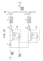
- Fig. 3 is a circuit diagram of an output stage of a first embodiment of a drive circuit according to the present invention
- Fig. 4 is an equivalent circuit of the output transistors and load for the circuit of Fig. 3.
- V H denotes a high supply voltage and V L a low supply voltage, with (V H - V L ) being the supply voltage of the output stage of the drive circuit.
- Numeral l denotes an inverter, 2 and 3 denote level shifters, 4 denotes a P-channel MOS FET and 5 an N- channel MOS FET. The following relationship is satisfied between the withstand voltage of the FETs 4 and 5 and the supply voltage (V H - V L ): (ON-state withstand voltage) ⁇ (V H - V L ) ⁇ (OFF-state withstand voltage).
- the level shifters 2 and 3 respectively serve to convert the level of the output signal from inverter l to appropriate gate input levels for the P-channel MOS FET 4 and N-channel MOS FET 5.
- R1 and R2 are resistors, respectively having one terminal connected to the source electrode of FET 4 and the source electrode of FET 5, and the other terminals thereof connected together to constitute an output terminal from which an output signal of the drive circuit is produced.
- 6 denotes a load, with one terminal thereof connected to the junction of resistors R1 and R2 and the other terminal thereof connected to a voltage V G .
- l4 denotes an equivalent circuit of the P-channel MOS FET 4 in Fig. 3
- l5 denotes an equivalent circuit for the N-channel MOS FET 5.
- R P and R N respectively denote the ON-state internal resistances of the FETs 4 and 5.
- S P and S N denote respective switches
- (I P ) M and (I N ) M denote respective peak currents of the FETs 4 and 5.
- I M is the smaller value of the currents (I P ) M and (I N ) M .
- R L is the value of resistance of load 6, for the case when load 6 is resistive.
- C L is the capacitance of load 6 when the load is capacitive.
- L L is the inductance of load 6 when the load is inductive.
- D1 and D2 are diodes which are connected when an inductive load is applied, for voltage absorption, with the other terminals of the diodes being connected to the voltages V H and V L respectively.
- the output signal goes to the V L potential when the input signal is at the "0" logic level, and goes to the V H value when the input signal is at the "l” logic level.
- the other FET will be in the OFF state, so that the applied voltage (V H - V L ) is applied to the OFF-state FET, and destructive voltage breakdown of the ON-state FET cannot occur.
- the P-channel MOS FET 4 and the N-channel MOS FET 5 may be instantaneously both in the ON state.
- R1 and R2 are selected such as to satisfy the following condition: [(V H - V L ) / (R1 + R2 + R P + R N )] ⁇ ⁇ I M ........(l) then most of the applied voltage (V H - V L ) will be developed across the resistors R1 and R2, so that destructive voltage breakdown of FETs 4 and 5 when these are in the ON state will not occur.
- the resistors R1 and R2 should be selected such as to satisfy both of the following relationships: [((V H - V L )) / (R1 + R P )] ⁇ ⁇ (I P ) M , [((V H - V L )) / (R2 + R N )] ⁇ ⁇ (I N ) M ..........(3)
- the load 6 can be considered to be a resistive load R L , such as that shown in Fig. 4, and since R L » R1, R2, the above relationship (l) will also apply in this case.
- resistors R1 and R2 are connected between the P-channel MOS FET 4 and N-channel MOS FET 5 which constitute an output stage, whereby even if the applied voltage (V H - V L ) is such that: (ON-state withstand voltage) ⁇ (V H - V L ) ⁇ (OFF-state withstand voltage) then destructive voltage breakdown will be prevented.
- the input and output signals of the circuit are of the same phase, and inverter l is incorporated for this reason. However if the input and output signals are required to be of opposite phase, then inverter l can be omitted. Furthermore in the above description it is assumed that the gate input levels of FETs 4 and 5 are different. However if the gate input levels of these FETs are identical, then level shifters 2 and 3 can be omitted.
- resistors are connected symmetrically between the P-channel MOS FET and the N-channel MOS FET, such that the voltage which is developed across these resistors when both of the FETs are momentarily set in the ON state is sufficient to prevent destructive voltage breakdown of the FETs, even when a supply voltage is applied to the push-pull output stage constituted by the FETs which is higher than the ON-state withstand voltage of the FETs and lower than the OFF-state withstand voltage of the FETs.
- Fig. 5 shows a second embodiment of the invention
- Fig. 6 is a timing chart for describing the operation of the circuit of Fig. 5.
- numeral. l denotes an inverter
- 2 and 3 denote level shifters
- 4 denotes a P-channel MOS FET
- 5 denotes 7 is an OR gate and 8 an AND gate.
- the rise-time and fall-time characteristics of FETs 4 and 5 are substantially identical.
- a high voltage V H is applied to the source electrode of FET 4 and a low voltage V L is applied to the source electrode of FET 5, with the voltages V H and V L being related to the withstand voltage characteristics of FETs 4 and 5 such that: (ON-state withstand voltage) ⁇ (V H - V L ) ⁇ (ON-state withstand voltage).
- the level shifters 2 and 3 have identical transfer characteristics, and in addition the rise and fall characteristics of the FETs 4 and 5 are also substantially identical.
- the P-channel MOS FET 4 goes to the ON state. In this way, the occurrence is prevented of a condition in which a voltage that is higher than the ON-state withstand voltage of the FETs is applied to a FET that is in the ON state, thereby ensuring that destructive voltage breakdown will not occur. This is illustrated by the timing chart of Fig. 6.
- a 2-input OR gate 7 is connected to the input of a P-channel MOS FET 4 while a 2-input AND gate 8 is connected to the input of an N-channel MOS FET 5, with an inverted drive input signal being applied to one input of each of the OR gate and AND gate and with the other input of each OR gate and AND gate being connected to the opposing output.
- the input and output signals of the circuit are of the same phase, and inverter l is incorporated for this reason. However if the input and output signals are required to be of opposite phase, then inverter l can be omitted.
- the gate input levels of FETs 2 and 3 are different. However if the gate input levels. of these FETs are identical, then level shifters 2 and 3 can be omitted.
- Fig. 7 is a circuit diagram of a drive circuit according to a third embodiment of the present invention
- Fig. 8 is a timing chart for describing the circuit of Fig. 7.
- numerals ll and 20 denote inverters
- numerals l2, l3, l5, and l6 through l8 denote buffer circuits
- l4 and l9 denote OR gates
- 4 denotes a P-channel MOS FET
- 5 an N-channel MOS FET.
- the rise time and fall time characteristics of the FETs 4 and 5 are substantially identical.
- Numerals 2 and 3 denote level shifters, for shifting the level of an input signal to the gate input levels of FETs 4 and 5 respectively.
- V H denotes a high supply voltage and V L a low supply voltage, which are respectively applied to the source electrodes of the P-channel MOS FET 4 and N-channel MOS FET 5.
- V H and V L must be related to the withstand voltage of FETs 4 and 5 as follows: (ON-state withstand voltage of FET) ⁇ (V H - V L ) ⁇ (OFF-state withstand voltage of FET)
- the operation of the circuit having the above configuration is as follows. Designating the signal transmission delay times of inverters ll and 20 as ⁇ 1, and the signal transmission delay times of the buffer circuits l2, l3, l5 and l6 to l8 as ⁇ 2, and the delay times of the OR gates l4 and l9 as ⁇ 3, then generally speaking ⁇ 1 ⁇ ⁇ ⁇ 2 ⁇ ⁇ ⁇ 3.
- the signal transmission delay time of the level shifters 2 and 3 will be designated as ⁇ 4.
- the output from OR gate l4 is delayed by an amount ( ⁇ 1 + 2 ⁇ 2 + ⁇ 3) before changing from the "l" logic level to the "0" logic level.
- the output from the level shifter 2 changes from the “l” logic level to the "0” logic level after a delay time of ( ⁇ 1 + 3 ⁇ 2 + ⁇ 3 + ⁇ 4).
- the output from the OR gate l9 changes from the "0" logic level to the “l” logic level after a delay time of ( ⁇ 2 + ⁇ 3) and the output from the inverter 20 changes from the "l” logic level to the "0” logic level after a delay time ( ⁇ 1 + ⁇ 2 + ⁇ 3).
- the output from the level shifter 3 therefore changes from the "l" logic level to the "0" logic level after a delay time of ( ⁇ 1 + ⁇ 2 + ⁇ 3 + ⁇ 4).
- the output from the level shifter 2 changes from the "l" logic level to the "0" logic level after a delay time of 2 ⁇ 2, that is to say when the input signal level changes from the "0" logic level to the "l” logic level
- the FET 5 first changes from the ON to the OFF state, then after a delay time of 2 ⁇ 2 the FET 4 changes from the OFF to the ON state. In this way, FETs 4 and 5 do not attain the ON condition simultaneously.
- the output from OR gate ll changes from the "l" logic level to the "0" logic level after a delay time of (3 ⁇ 2 + ⁇ 3)
- the output from the level shifter 3 changes from the "0" logic level to the "l” logic level after a delay time of ( ⁇ 1 + 3 ⁇ 2 + ⁇ 3 + ⁇ 4). Comparing the delay times of the outputs from level shifters 2 and 3, the output from the level shifter 3 is delayed by an amount 2 ⁇ 2 with respect to the output from the level shifter 2, in changing from the "0" logic level to the "l” logic level.
- the FET 4 first changes from the ON to the OFF state, then after a delay time of 2 ⁇ 2 the FET 5 changes from the OFF to the ON state. As a result, a condition is avoided whereby both of FETs 4 and 5 are simultaneously in the ON state.
- pairs of buffers i.e. buffers l2 and l3 and buffers l7 and l8 are used to establish delay times.
- pairs of buffers i.e. buffers l2 and l3 and buffers l7 and l8 are used to establish delay times.
- single buffers rather than pairs, or sets of 3 or more buffers.
- Fig. 9 illustrates a delay circuit for a fourth embodiment of the present invention, in which such a resistance-capacitance delay circuit is used to provide a substantially long value of delay time.
- one-shot multivibrators may be utilized to provide a longer value of delay time, in place of the buffer circuits l2 l3, and l7, l8.
- Fig. l0 shows a fifth embodiment of the present invention, in which this is done.
- Figs. ll and l2 respectively show a sixth and a seventh embodiment of the present invention, in which delay circuits are utilized which operate on the basis of a clock signal.
- the delay circuit is formed of a data-type flip-flop 25, having a clock input terminal which is coupled to receive a clock signal, referred to in the following as the delay clock signal, from a clock signal source (not shown in the drawing), and a data terminal coupled to receive the inverted drive input signal from inverter ll.
- the Q output from D-type flip-flop 25 is applied to one input terminal of the OR gate l4 and the output from inverter ll to the input of OR gate l4.
- a D-type flip-flop 26 is coupled to receive the delay clock signal and the drive input signal.
- the output from D-type flip-flop 26 is applied to one input terminal of a NOR gate 27, and the drive input signal to the other input of NOR gate 27, with the output from NOR gate 27 being applied to the input of level shifter 3.
- a delay gate circuit 28 is controlled by a delay clock signal, and is coupled to receive the inverted input drive signal from inverter ll and to apply an output signal to the OR gate l4.
- a delay gate circuit based on a pair of FETs coupled to a capacitor C, and an inverter for applying gate input signals of mutually opposite phase to the FETs, is well known in the art and so detailed description will be omitted.
- a similar delay gate circuit 29 is coupled to receive the input drive signal and the delay clock signal, and applies an output signal to one input terminal of a NOR gate 27, while the input drive signal is applied to the other input of NOR gate 27.
- the output from NOR gate 27 is applied to level shifter 3. It will be apparent that the delay amount ⁇ (described hereinabove referring to Fig. 8) produced by this embodiment will be equal to one period of the delay clock signal.
- a push-pull circuit which is formed of a P-channel MOS FET 4 and an N-channel MOS FET 5, with input signals of identical logic level being applied to the gate electrodes of the P-channel MOS FET 4 and N-channel MOS FET 5, together with a circuit which produces a fixed delay before a rising edge of the drive input signal level is applied as a falling edge of the input signal of the gate electrode of the P channel MOS FET, and a circuit which produces a fixed delay before a falling edge of of the drive input signal is applied as a rising edge of the input signal of the gate electrode of the N-channel MOS FET.
Landscapes
- Physics & Mathematics (AREA)
- Engineering & Computer Science (AREA)
- Computer Hardware Design (AREA)
- Computing Systems (AREA)
- General Engineering & Computer Science (AREA)
- Mathematical Physics (AREA)
- Logic Circuits (AREA)
Applications Claiming Priority (6)
| Application Number | Priority Date | Filing Date | Title |
|---|---|---|---|
| JP61214381A JPS6369316A (ja) | 1986-09-11 | 1986-09-11 | Mos型fetを用いた駆動回路 |
| JP214381/86 | 1986-09-11 | ||
| JP61269057A JPS63122319A (ja) | 1986-11-12 | 1986-11-12 | 駆動回路 |
| JP61269054A JPS63122318A (ja) | 1986-11-12 | 1986-11-12 | 駆動回路 |
| JP269054/86 | 1986-11-12 | ||
| JP269057/86 | 1986-11-12 |
Publications (1)
| Publication Number | Publication Date |
|---|---|
| EP0264614A1 true EP0264614A1 (fr) | 1988-04-27 |
Family
ID=27329607
Family Applications (1)
| Application Number | Title | Priority Date | Filing Date |
|---|---|---|---|
| EP87113349A Ceased EP0264614A1 (fr) | 1986-09-11 | 1987-09-11 | Circuit d'attaque MOSFET fournissant protection contre la rupture dûe aux tensions transitoires |
Country Status (2)
| Country | Link |
|---|---|
| US (1) | US4825102A (fr) |
| EP (1) | EP0264614A1 (fr) |
Cited By (6)
| Publication number | Priority date | Publication date | Assignee | Title |
|---|---|---|---|---|
| EP0351820A2 (fr) * | 1988-07-19 | 1990-01-24 | Kabushiki Kaisha Toshiba | Circuit de sortie |
| EP0373693A2 (fr) * | 1988-12-15 | 1990-06-20 | STMicroelectronics S.r.l. | Générateur de signaux de commande pour transistors connectés en une configuration en demi-pont |
| EP0397241A1 (fr) * | 1989-05-09 | 1990-11-14 | Koninklijke Philips Electronics N.V. | Excitateur pour circuits de demi-pont à tension élevée |
| KR960003053A (ko) * | 1994-06-17 | 1996-01-26 | 카렌 지. 핑크 | 브리지 제어 회로 및 방법 |
| WO2001048925A1 (fr) * | 1999-12-28 | 2001-07-05 | Honeywell Inc. | Circuits et procede destines a eliminer des pics dans des circuits numeriques |
| EP1982413A1 (fr) * | 2006-02-06 | 2008-10-22 | Mosaid Technologies Incorporated | Circuit de dispositif de décalage de niveau de tension |
Families Citing this family (20)
| Publication number | Priority date | Publication date | Assignee | Title |
|---|---|---|---|---|
| US4990802A (en) * | 1988-11-22 | 1991-02-05 | At&T Bell Laboratories | ESD protection for output buffers |
| US5075569A (en) * | 1989-03-17 | 1991-12-24 | Tektronix, Inc. | Output device circuit and method to minimize impedance fluctuations during crossover |
| IT1229318B (it) * | 1989-05-02 | 1991-08-08 | Sgs Thomson Microelectronics | Dispositivo di protezione contro il breakdown di transistori bipolari in un circuito integrato di pilotaggio per dispositivo di potenza con carico risonante sul collettore. |
| JPH03169273A (ja) * | 1989-11-22 | 1991-07-22 | Mitsubishi Electric Corp | スイッチングデバイス駆動回路 |
| JPH04130770A (ja) * | 1990-09-21 | 1992-05-01 | Mitsubishi Electric Corp | 半導体集積回路 |
| US5155392A (en) * | 1990-11-05 | 1992-10-13 | Motorola, Inc. | Low di/dt BiCMOS output buffer with improved speed |
| US5233238A (en) * | 1991-12-20 | 1993-08-03 | Vlsi Technology, Inc. | High power buffer with increased current stability |
| US5300832A (en) * | 1992-11-10 | 1994-04-05 | Sun Microsystems, Inc. | Voltage interfacing buffer with isolation transistors used for overvoltage protection |
| US5331593A (en) * | 1993-03-03 | 1994-07-19 | Micron Semiconductor, Inc. | Read circuit for accessing dynamic random access memories (DRAMS) |
| US5426376A (en) * | 1993-04-23 | 1995-06-20 | Vlsi Technology, Inc. | Noise isolated I/O buffer that uses two separate power supplies |
| US5736997A (en) * | 1996-04-29 | 1998-04-07 | Lexmark International, Inc. | Thermal ink jet printhead driver overcurrent protection scheme |
| US6294939B1 (en) * | 1998-10-30 | 2001-09-25 | Stmicroelectronics, Inc. | Device and method for data input buffering |
| US6603338B1 (en) | 1998-10-30 | 2003-08-05 | Stmicroelectronics, Inc. | Device and method for address input buffering |
| US6547353B2 (en) * | 1999-07-27 | 2003-04-15 | Stmicroelectronics, Inc. | Thermal ink jet printhead system with multiple output driver circuit for powering heating element and associated method |
| TW503620B (en) * | 2000-02-04 | 2002-09-21 | Sanyo Electric Co | Drive apparatus for CCD image sensor |
| US6481814B2 (en) | 2001-02-28 | 2002-11-19 | Lemark International, Inc. | Apparatus and method for ink jet printhead voltage fault protection |
| US20050275027A1 (en) * | 2003-09-09 | 2005-12-15 | Micrel, Incorporated | ESD protection for integrated circuits |
| JP2006279883A (ja) * | 2005-03-30 | 2006-10-12 | Sanyo Electric Co Ltd | ドライバ回路 |
| US20070063758A1 (en) * | 2005-09-22 | 2007-03-22 | Honeywell International Inc. | Voltage divider and method for minimizing higher than rated voltages |
| US8226190B2 (en) * | 2008-12-01 | 2012-07-24 | Canon Kabushiki Kaisha | Recording element substrate and recording head having the same |
Citations (4)
| Publication number | Priority date | Publication date | Assignee | Title |
|---|---|---|---|---|
| US3651340A (en) * | 1970-06-22 | 1972-03-21 | Hamilton Watch Co | Current limiting complementary symmetry mos inverters |
| US4164842A (en) * | 1976-08-20 | 1979-08-21 | Citizen Watch Co., Ltd. | Buffer amplifier circuit |
| US4467224A (en) * | 1982-03-18 | 1984-08-21 | Rca Corporation | System for applying a high voltage source to a CRT through a capacitive load |
| US4540904A (en) * | 1983-05-03 | 1985-09-10 | The United States Of America As Represented By The Secretary Of The Air Force | Tri-state type driver circuit |
Family Cites Families (10)
| Publication number | Priority date | Publication date | Assignee | Title |
|---|---|---|---|---|
| JPS5386151A (en) * | 1977-01-06 | 1978-07-29 | Nec Corp | Complementary field effect transistor circuit |
| JPS53114651A (en) * | 1977-03-17 | 1978-10-06 | Fujitsu Ltd | Electronic circuit |
| US4103190A (en) * | 1977-03-25 | 1978-07-25 | Motorola, Inc. | Complementary power saving comparator/inverter circuits |
| JPS5432259A (en) * | 1977-08-18 | 1979-03-09 | Toshiba Corp | Complementary pair circuit of transistor |
| JPS5612128A (en) * | 1979-07-12 | 1981-02-06 | Toshiba Corp | Cmos buffer circuit |
| JPS5763861A (en) * | 1980-10-06 | 1982-04-17 | Nec Corp | Semiconductor device |
| JPS58121829A (ja) * | 1982-01-14 | 1983-07-20 | Nippon Telegr & Teleph Corp <Ntt> | 駆動回路 |
| JPS58142626A (ja) * | 1982-02-18 | 1983-08-24 | Toshiba Corp | 出力バツフア回路 |
| US4525635A (en) * | 1982-12-15 | 1985-06-25 | Rca Corporation | Transient signal suppression circuit |
| US4620310A (en) * | 1985-03-11 | 1986-10-28 | Metapath Inc. | Method and apparatus for generating bipolar pulses in a local area network |
-
1987
- 1987-09-11 US US07/095,457 patent/US4825102A/en not_active Expired - Lifetime
- 1987-09-11 EP EP87113349A patent/EP0264614A1/fr not_active Ceased
Patent Citations (4)
| Publication number | Priority date | Publication date | Assignee | Title |
|---|---|---|---|---|
| US3651340A (en) * | 1970-06-22 | 1972-03-21 | Hamilton Watch Co | Current limiting complementary symmetry mos inverters |
| US4164842A (en) * | 1976-08-20 | 1979-08-21 | Citizen Watch Co., Ltd. | Buffer amplifier circuit |
| US4467224A (en) * | 1982-03-18 | 1984-08-21 | Rca Corporation | System for applying a high voltage source to a CRT through a capacitive load |
| US4540904A (en) * | 1983-05-03 | 1985-09-10 | The United States Of America As Represented By The Secretary Of The Air Force | Tri-state type driver circuit |
Non-Patent Citations (7)
| Title |
|---|
| ELECTRONIC DESIGN, 18th April 1985, pages 52, 53; D. BURSKY: "CMOS ICs handle high-voltage needs of RS-232 interface" * |
| PATENT ABSTRACTS OF JAPAN, vol. 2, no. 120, page 6968 (E78), 16th October 1978, ; & JP - A - 53 86151 (NIPPON DENKI K.K.) 29-07-1978 * |
| PATENT ABSTRACTS OF JAPAN, vol. 3, no. 54, page 28 (E109), 10th May 1979; & JP - A - 54 32259 (TOKYO SHIBAURA DENKI K.K.) 09-03-1979 * |
| PATENT ABSTRACTS OF JAPAN, vol. 5, no. 63 (E-54)[735], 28th April 1981; & JP - A - 56 12128 (TOKYO SHIBAURA DENKI K.K.) 06-02-1981 * |
| PATENT ABSTRACTS OF JAPAN, vol. 6, no. 140 (E-121)[1018], 29th July 1982; & JP - A - 57 63861 (NIPPON DENKI K.K.) 17-04-1982 * |
| PATENT ABSTRACTS OF JAPAN, vol. 7, no. 233 (E-204)[1378], 15th October 1983; & JP - A - 58 121 829 (NIPPON DENSHIN DENWA KOSHA) 20-07-1983 * |
| PATENT ABSTRACTS OF JAPAN, vol.7, no. 258 (E-211)[1403], 17th November 1983; & JP - A - 58 142 626 (TOKYO SHIBAURA DENKI K.K.) 24-08-1983 * |
Cited By (12)
| Publication number | Priority date | Publication date | Assignee | Title |
|---|---|---|---|---|
| EP0351820A2 (fr) * | 1988-07-19 | 1990-01-24 | Kabushiki Kaisha Toshiba | Circuit de sortie |
| EP0351820A3 (en) * | 1988-07-19 | 1990-05-30 | Kabushiki Kaisha Toshiba | Output circuit |
| US4996449A (en) * | 1988-07-19 | 1991-02-26 | Kabushiki Kaisha Toshiba | Output circuit having high speed operation and low power dissipation |
| EP0373693A2 (fr) * | 1988-12-15 | 1990-06-20 | STMicroelectronics S.r.l. | Générateur de signaux de commande pour transistors connectés en une configuration en demi-pont |
| EP0373693A3 (en) * | 1988-12-15 | 1990-10-31 | Sgs-Thomson Microelectronics S.R.L. | Generator of drive signals for transistors connected in a half-bridge configuration |
| EP0397241A1 (fr) * | 1989-05-09 | 1990-11-14 | Koninklijke Philips Electronics N.V. | Excitateur pour circuits de demi-pont à tension élevée |
| US4989127A (en) * | 1989-05-09 | 1991-01-29 | North American Philips Corporation | Driver for high voltage half-bridge circuits |
| KR960003053A (ko) * | 1994-06-17 | 1996-01-26 | 카렌 지. 핑크 | 브리지 제어 회로 및 방법 |
| WO2001048925A1 (fr) * | 1999-12-28 | 2001-07-05 | Honeywell Inc. | Circuits et procede destines a eliminer des pics dans des circuits numeriques |
| US6356101B1 (en) | 1999-12-28 | 2002-03-12 | Honeywell International Inc. | Glitch removal circuitry |
| EP1982413A1 (fr) * | 2006-02-06 | 2008-10-22 | Mosaid Technologies Incorporated | Circuit de dispositif de décalage de niveau de tension |
| EP1982413A4 (fr) * | 2006-02-06 | 2010-05-26 | Mosaid Technologies Inc | Circuit de dispositif de décalage de niveau de tension |
Also Published As
| Publication number | Publication date |
|---|---|
| US4825102A (en) | 1989-04-25 |
Similar Documents
| Publication | Publication Date | Title |
|---|---|---|
| EP0264614A1 (fr) | Circuit d'attaque MOSFET fournissant protection contre la rupture dûe aux tensions transitoires | |
| US5896045A (en) | Static pulsed cross-coupled level shifter and method therefor | |
| US4695744A (en) | Level shift circuit including source follower output | |
| KR100218506B1 (ko) | 액정 표시 장치용 레벨 시프트 회로 | |
| KR920004341B1 (ko) | 반도체집적회로의 출력회로 | |
| US7068091B1 (en) | Voltage translator circuit formed using low voltage transistors | |
| JPS59108426A (ja) | 結合用中間回路 | |
| US4437024A (en) | Actively controlled input buffer | |
| US6184716B1 (en) | High voltage output stage for driving an electric load | |
| JP2006270382A (ja) | レベルシフト回路および電源装置 | |
| US9473116B1 (en) | Low-cost, capacitive-coupled level shifter scalable for high-voltage applications | |
| EP3732789A1 (fr) | Décaleur de niveau insensible aux transitions | |
| EP0872956B1 (fr) | Circuit de verrouillage capable de réduire le courant transversal | |
| US4406957A (en) | Input buffer circuit | |
| JPH06153533A (ja) | レベルシフト回路及びこれを用いたインバータ装置 | |
| CA2089429C (fr) | Tampon d'entree ttl-cmos eliminateur de bruit a faible consommation d'energie | |
| US6717456B2 (en) | Level conversion circuit | |
| AU593454B2 (en) | Apparatus and method for capacitor coupled complementary buffering | |
| EP0810732A2 (fr) | Circuit générateur de signaux différentiels ayant un circuit de suppression de pics de courant | |
| US5699000A (en) | Output buffer circuit for a semiconductor IC | |
| US3892985A (en) | Set-preferring R-S flip-flop circuit | |
| US11165426B1 (en) | Level shifter and a method of level shifting a signal | |
| JP2593872B2 (ja) | レベル変換回路 | |
| JPH07105709B2 (ja) | 電圧変換回路 | |
| CN221010085U (zh) | 一种电平移位电路、驱动芯片以及电子设备 |
Legal Events
| Date | Code | Title | Description |
|---|---|---|---|
| PUAI | Public reference made under article 153(3) epc to a published international application that has entered the european phase |
Free format text: ORIGINAL CODE: 0009012 |
|
| 17P | Request for examination filed |
Effective date: 19870911 |
|
| AK | Designated contracting states |
Kind code of ref document: A1 Designated state(s): DE FR GB |
|
| 17Q | First examination report despatched |
Effective date: 19900525 |
|
| STAA | Information on the status of an ep patent application or granted ep patent |
Free format text: STATUS: THE APPLICATION HAS BEEN REFUSED |
|
| 18R | Application refused |
Effective date: 19930807 |
|
| RIN1 | Information on inventor provided before grant (corrected) |
Inventor name: IWASAWA, TOSHIYUKI Inventor name: MIURA, MASAYOSHI |