EP0350879A2 - Ausgangstreiberschaltung für Halbleiter-IC - Google Patents
Ausgangstreiberschaltung für Halbleiter-IC Download PDFInfo
- Publication number
- EP0350879A2 EP0350879A2 EP89112693A EP89112693A EP0350879A2 EP 0350879 A2 EP0350879 A2 EP 0350879A2 EP 89112693 A EP89112693 A EP 89112693A EP 89112693 A EP89112693 A EP 89112693A EP 0350879 A2 EP0350879 A2 EP 0350879A2
- Authority
- EP
- European Patent Office
- Prior art keywords
- mos transistor
- gate
- output
- output buffer
- supply potential
- Prior art date
- Legal status (The legal status is an assumption and is not a legal conclusion. Google has not performed a legal analysis and makes no representation as to the accuracy of the status listed.)
- Granted
Links
Images


Classifications
-
- G—PHYSICS
- G11—INFORMATION STORAGE
- G11C—STATIC STORES
- G11C7/00—Arrangements for writing information into, or reading information out from, a digital store
- G11C7/10—Input/output [I/O] data interface arrangements, e.g. I/O data control circuits, I/O data buffers
- G11C7/1051—Data output circuits, e.g. read-out amplifiers, data output buffers, data output registers, data output level conversion circuits
- G11C7/1057—Data output buffers, e.g. comprising level conversion circuits, circuits for adapting load
-
- G—PHYSICS
- G11—INFORMATION STORAGE
- G11C—STATIC STORES
- G11C7/00—Arrangements for writing information into, or reading information out from, a digital store
- G11C7/10—Input/output [I/O] data interface arrangements, e.g. I/O data control circuits, I/O data buffers
- G11C7/1051—Data output circuits, e.g. read-out amplifiers, data output buffers, data output registers, data output level conversion circuits
-
- H—ELECTRICITY
- H03—ELECTRONIC CIRCUITRY
- H03K—PULSE TECHNIQUE
- H03K19/00—Logic circuits, i.e. having at least two inputs acting on one output; Inverting circuits
- H03K19/0008—Arrangements for reducing power consumption
- H03K19/0013—Arrangements for reducing power consumption in field effect transistor circuits
-
- H—ELECTRICITY
- H03—ELECTRONIC CIRCUITRY
- H03K—PULSE TECHNIQUE
- H03K19/00—Logic circuits, i.e. having at least two inputs acting on one output; Inverting circuits
- H03K19/003—Modifications for increasing the reliability for protection
- H03K19/00346—Modifications for eliminating interference or parasitic voltages or currents
- H03K19/00361—Modifications for eliminating interference or parasitic voltages or currents in field effect transistor circuits
-
- H—ELECTRICITY
- H03—ELECTRONIC CIRCUITRY
- H03K—PULSE TECHNIQUE
- H03K19/00—Logic circuits, i.e. having at least two inputs acting on one output; Inverting circuits
- H03K19/01—Modifications for accelerating switching
- H03K19/017—Modifications for accelerating switching in field-effect transistor circuits
- H03K19/01707—Modifications for accelerating switching in field-effect transistor circuits in asynchronous circuits
-
- G—PHYSICS
- G11—INFORMATION STORAGE
- G11C—STATIC STORES
- G11C2207/00—Indexing scheme relating to arrangements for writing information into, or reading information out from, a digital store
- G11C2207/10—Aspects relating to interfaces of memory device to external buses
- G11C2207/108—Wide data ports
Definitions
- the present invention relates to integrated circuits, and more particularly to an output buffer circuit.
- a data output circuit, or an output buffer circuit, for driving an external load of a large capacitance, is used as a circuit for outputting the data generated in a semiconductor integrated circuit (referred to as an IC) to exterior.
- IC semiconductor integrated circuit
- the output buffer circuit is generally provided with an input node and an output node, and output transistors that are conductive in response to a signal applied to the input node.
- the load capacitor connected to the output node is charged or discharged to a power source voltage through the conducting output transistors.
- Such output transistors have an extremely large current drive ability to charge or discharge in a short time the load capacitor of a large amount, for example, 100 pF.
- the power source voltage and the ground voltage are supplied through wires to the IC in a package.
- a large current flows through the wires.
- the large rate of change in drive current can induce a large voltage drop across the inductances of the wires and the package.
- the resulting noise in the internal power source voltage and the ground voltage causes an erroneous operation of the IC.
- an object of the present invention is to provide an output buffer circuit which minimizes the occurrence of the erroneous operation of an IC by reducing a voltage drop due to charging or discharging of an external load capacitance.
- the output buffer circuit for producing an output data at an output terminal comprising: a first MOS transistor for charging the output terminal toward a first supply potential when the first MOS transistor turned on, the first MOS transistor having a gate, a source and a drain, the source and drain connection between the output terminal and a first supply potential terminal; a second MOS transistor for discharging the output terminal toward a second supply potential when the second MOS transistor turned on, the second MOS transistor having a gate, a source and a drain, the source and drain of the second MOS transistor connected between the output terminal and a second supply potential terminal; and a resistance means for charging the gate of the second MOS transistor toward the first supply potential when turned on, the resistance means connected between the first supply potential terminal and the gate of the second MOS transistor, the resistance means having nearly a constant value.
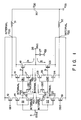
- FIG. 1 showing a circuit arrangement of an output buffer (a data output circuit) according to a first embodiment of the present invention.
- Data Dout′ generated in a semiconductor integrated circuit is supplied to an input node 11 of the output buffer according to the present invention.
- the data Dout′ received at the input node 11 is applied to a NOR gate G1 and a NAND gate G2.
- the NOR gate G1 is formed by P-channel transistors 12 and 14, and N-channel transistors 13 and 15.
- the NAND gate G2 is formed by P-channel transistors 20 and 21 and n-channel transistors 19 and 22.
- a control signal OD1 is applied to the NOR gate G1.
- Another control signal OD2 is applied to the NOR gate G2.
- An output signal of the NOR gate G1 is applied to an inverter IN1 formed by a P-channel transistor 16 and an N-channel transistor 17.
- An output signal of the NAND gate G2 is applied to an inverter IN2 formed by a P-channel transistor 23 and an N-channel transistor 24.
- An output signal of the inverter IN1 is applied to the gate of a P-channel transistor 18 (referred to as an output transistor) constituting an output stage.
- An output signal of the inverter IN2 is applied to the gate of an N-channel transistor 25 (referred to as an output transistor) constituting an output stage.
- the source of the output transistor 18 is connected to internal power source voltage V DD , and its drain is connected to an output node 26.
- the source of the output transistor 25 is connected to internal ground voltage V SS , and its drain is connected to the output node 26.
- the output node 26 is coupled with a load capacitor 27.
- a resistance 28 is connected between the drain of the transistor 23 in the inverter IN2 and the gate of the output transistor 25.
- This resistance 28 is formed with a polysilicon layer or a diffusion layer.
- reference numeral 30 designates an external power source.
- Reference numeral 31 represents lead inductance between the output buffer and V DD (power source 30).
- Reference numeral 32 represents lead inductance between the output buffer and V SS (ground, power source 30).
- the element size, e.g., the channel width, of each output transistor 18 and 25 is large, in order to achieve high drive currents.
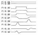
- Figs. 2A and 2B shows waveforms of the control signals OD1 (a logic “0") and OD2 (a logic “1”);
- Fig. 2C a waveform of the data signal Dout′ supplied to the input node 11;
- Fig. 2D a waveform of the voltage at the gate node "a” of the output transistor 18;
- Fig. 2E a waveform of the voltage at the gate node “b” of the output transistor 25;
- Fig. 2F a waveform of the output node 26;
- Fig. 2G a waveform of the drain current of the output transistor 18;
- Fig. 2H a waveform of the drain current of the output transistor 25;
- Figs.2I and 2J waveforms of the internal power source voltage V DD and the internal ground voltage V SS .
- the gate voltages of the output transistors 18 and 25 change to be switched.
- the drain current Is of the output transistor 18 or the drain current It of another output transistor 25 flows.
- the current flow causes a voltage drop across the inductance 31 or 32, as shown in Figs. 2I and 2J.
- Fig. 6 shows an arrangement of a semiconductor memory incorporating an output buffer circuit according to the present invention.
- the semiconductor memory is made up of a row decoder (RD) 110 coupled with input buffer circuit (IB) 108 to which row address input signals are supplied, a plurality of memory cell arrays (MCA) 1141 to 114 n coupled with the row decoder (RD) 110 through row lines 112, a plurality of column select circuits (CSC) 1181 to 118 n coupled with the memory cell arrays (MCA) 1141 to 114 n through column lines 116, a column decoder (CD) 120 that is coupled with the column select circuits (CSC) 1181 to 118 n , and the column decoder 120 is applied output signals from another input buffer circuit (IB) 109 to which column address signals are applied.
- RD row decoder
- IB input buffer circuit
- a plurality of sense amplifiers (SA) 1221 to 122 n are coupled with the column select circuits (CSC) 1181 to 118 n , respectively.
- a plurality of output buffer circuits (OB) 1241 to 124 n are coupled with the sense amplifiers (SA) 1221 to 122 n .
- the output terminals of the output buffer circuits (OB) 1241 to 124 n are coupled with output terminals.
- the change of the internal voltage V DD and the internal voltage V SS is caused inside the IC that is outputting data from the output buffer circuits 1241 to 124 n .
- the address signals are applied to the input buffer circuits 108 and 109 from an another IC (not shown). Accordingly, even if the internal voltages V DD and V SS change within the IC outputting data, the voltage level of the address signal does not change. It is assumed now that the address signal of a logic "0" is supplied to the IC.
- the input buffer circuits 108 and 109 of this IC applying the internal voltage V SS as a reference potential sometimes mistakenly recognizes the "0" input data as "1" data.
- FIG. 5 A graphical representation of the relation (3) is illustrated in Fig. 5.
- the x-coordinate axis represents V G - V T and the y-coordinate, dI D /dt.
- the relation (3) is expressed by a straight line Y inclined by an angle of ⁇ a. As seen, as the gate voltage V G increases, the dI D /dt increases. When the V G - V T reaches A, e.g., +5 V, the dI D /dt reaches a value of B.
- the straight line X increases with the inclination of ⁇ 2a up to point C.
- the dI D /dt increases with the inclination of ⁇ (1/2) ⁇ a.
- a value of the dI D /dt at point A on the V G - V T axis is equal to that when the dI D /dt changes along the straight line Y.
- the time taken to reach point A is shorter because the dI D /dt changes above the line Y.
- the charge speed can be increased with keeping dI D /dt of B in the following way.
- the output buffer circuit according to the present invention has the resistance 28 inserted between the gate of the transistor 25 constituting the output stage and the drain of the transistor 23 in the inverter IN2 for driving the gate of the output transistor 25 (see Fig. 1).
- the gate voltage of the output transistor 25 rises and transiently changes from an on-state to an off-state, the charge to the node "b" is performed in the following way. In the region where the gate voltage is low (di/dt of the current of the output transistor 25 is small), the node “b” is rapidly charged. In the region where the gate voltage is high (the di/dt is large), the node "b” is gently charged because of the presence of the resistance 28.
- the discharging speed of the output node 26 is faster if the di/dt of the present circuit is equal to that of the conventional one. If the discharging speed is the same, the di/dt of the present circuit becomes small compared with that of the conventional one, which leads to a smaller change of internal V SS .
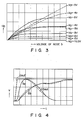
- FIG. 3 A relationship of the voltage of the node b (Fig. 1) vs. drain current I D of the transistor 23 is depicted in Fig. 3, with the gate voltage V G of the transistor 23 as a parameter.
- the source of the transistor was fixed at the ground voltage V SS , and the voltage of the node b was increased from 0 V toward the negative polarity.
- solid curves represent the characteristic curves of the transistor 23 in the conventional case.
- the curves of broken lines represent the characteristic curves of a circuit of the invention which is formed by the transistor 23 and the resistance 28 connected in series with the transistor 23.
- the circuit becomes to exhibit a constant resistance.
- the current I D of the transistor 23 coupled with the resistor 28 is more restricted than that of the transistor 23 not coupled with the resistance 28.
- the drain current I D flows more than that of the transistor 23 not coupled with the resistance 28.
- the circuit is greatly influenced by the characteristic of the resistance 28, so that the I D - V D characteristic is more linear.
- the conduction resistance of the transistor 23 connected to the resistance 28 is smaller than that of the conventional transistor without the resistance 28.
- the conduction resistance of the transistor 23 is about 10 k ⁇ which is measured by applying -5 V to the gate and drain of the transistor 23.
- the resistance 28 and the transistor 23 are approximately the same in resistance value.
- the gate insulating layer thickness is 280 ⁇
- the threshold voltage is -1 V
- the channel width and length are 14.7 ⁇ m and 3.7 ⁇ m, respectively.
- the transistor 23 used in the conventional output buffer circuit has the channel width and length of 7.2 ⁇ m and 3.7 ⁇ m, respectively.
- the potential difference between the node b and the internal voltage V DD becomes gradually small. Accordingly, under the same voltage of the node b as that of the conventional circuit, the current becomes small as indicated by broken lines. Under this condition, the charging speed at the gate of the output transistor 25 is slower than that in the conventional circuit.
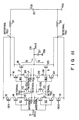
- Fig. 4 there are plotted voltage variations at the nodes “a” and “b” (the gates of the output transistors 18 and 25) in the output buffer circuit of the instant invention and the conventional one.
- the voltage variations indicated by solid lines are those of the conventional output buffer circuit.
- the voltage variations indicated by broken lines are those of the output buffer circuit according to the instant invention.
- the voltage Vb at the node “b” in low voltages more rapidly charges the gate of the output transistor 25 than that indicated by a solid line in the conventional circuit.
- the charging rate of the gate of the transistor 25 becomes slower than the corresponding voltage indicated by a solid line in the conventional circuit.
- the node "b" is more rapidly charged than the corresponding one in the conventional circuit. Accordingly, the load capacitor 27 coupled with the output node 26 is more rapidly discharged.
- the peak value of the di/dt is equal to that of the conventional circuit.
- the di/dt of the discharge current flowing through the output transistor 25 and its peak current can be set to be smaller than those of the conventional circuit. This fact indicates that the change of the internal ground voltage V SS can be smaller than that of the conventional circuit, and consequently that it is possible to prevent the erroneous operation of the IC due to the change of the internal ground voltage.
- the present invention is not limited to the above specific embodiment, but may be variously changed and modified within the spirit of the present invention.
- the resistance 28 inserted between the drain of the transistor 23 and the gate of the output transistor 25 may be substituted by another resistive element in order to reduce element size.
- an N-channel depletion-type MOS transistor 41 is used in place of the resistance 28. In this instance, the data Dout′ is applied to the gate of the transistor 41. If necessary, the voltage V DD is applied to the gate of the transistor 41.
- the resistance 28 is replaced by two transistors, N-channel depletiontype MOS transistor 41′, and N-channel enhancement-type MOS transistor 42.
- the source-drain paths of the two transistors are coupled in parallel with each other.
- only the transistor 42 may be used as in a fourth embodiment of Fig. 9.
- Fig. 10 shows the drain current I D vs. the voltage of node b characteristic curves, with a parameter of the gate voltage V G of the transistor 23, when the depletion-type MOS transistor 41 is used, as shown in Fig. 7.
- the source of the transistor 23 is connected to the ground, and the voltage of the node b is increased from 0 V toward the negative polarity.
- the characteristic curves show that more drain current flows when the voltage is small, compared with the case where the resistance 28 is used, and that less drain current flows for a large drain voltage. Therefore, the use of the transistor 41 renders the operation of an output buffer circuit according to the invention more effective.
- the resistance 28 is connected between the drain of the transistor 23 and the gate of the output transistor 25
- another resistance 29 can be inserted between the drain of the N-channel transistor 17 and the gate of the output transistor 18, as shown in Fig. 11 showing a fifth embodiment of the present invention.
- the instant embodiment reduces a change of the internal power source voltage V DD , further improving the characteristics of the output buffer circuit.
- an output buffer circuit according to the present invention is so arranged that the current flowing into the output transistor is controlled by using a resistive element. With such an arrangement, a potential change of the internal power voltage caused by charging or discharging of an external load capacitance can be minimized with a fast speed of the charging or discharging.
Landscapes
- Physics & Mathematics (AREA)
- Engineering & Computer Science (AREA)
- Computer Hardware Design (AREA)
- Computing Systems (AREA)
- General Engineering & Computer Science (AREA)
- Mathematical Physics (AREA)
- Logic Circuits (AREA)
- Semiconductor Integrated Circuits (AREA)
- Metal-Oxide And Bipolar Metal-Oxide Semiconductor Integrated Circuits (AREA)
- Electronic Switches (AREA)
Applications Claiming Priority (2)
| Application Number | Priority Date | Filing Date | Title |
|---|---|---|---|
| JP172321/88 | 1988-07-11 | ||
| JP63172321A JP2573320B2 (ja) | 1988-07-11 | 1988-07-11 | 出力バッファ回路 |
Publications (3)
| Publication Number | Publication Date |
|---|---|
| EP0350879A2 true EP0350879A2 (de) | 1990-01-17 |
| EP0350879A3 EP0350879A3 (en) | 1990-05-30 |
| EP0350879B1 EP0350879B1 (de) | 1993-07-07 |
Family
ID=15939745
Family Applications (1)
| Application Number | Title | Priority Date | Filing Date |
|---|---|---|---|
| EP89112693A Expired - Lifetime EP0350879B1 (de) | 1988-07-11 | 1989-07-11 | Ausgangstreiberschaltung für Halbleiter-IC |
Country Status (5)
| Country | Link |
|---|---|
| US (1) | US4985646A (de) |
| EP (1) | EP0350879B1 (de) |
| JP (1) | JP2573320B2 (de) |
| KR (1) | KR920010984B1 (de) |
| DE (1) | DE68907451T2 (de) |
Cited By (5)
| Publication number | Priority date | Publication date | Assignee | Title |
|---|---|---|---|---|
| EP0410473A3 (en) * | 1989-07-28 | 1991-07-31 | Kabushiki Kaisha Toshiba | Semiconductor integrated circuit |
| EP0487212A3 (en) * | 1990-11-23 | 1992-09-02 | Ncr Corporation | Integrated circuit having noise control means |
| EP0464468A3 (en) * | 1990-06-22 | 1993-03-31 | Kabushiki Kaisha Toshiba | Semiconductor memory device |
| WO1993026091A1 (en) * | 1992-06-12 | 1993-12-23 | Seiko Epson Corporation | System and method for reducing ground bounce in integrated circuit output buffers |
| EP0511858A3 (de) * | 1991-05-01 | 1995-02-15 | Winbond Electronics North Amer |
Families Citing this family (12)
| Publication number | Priority date | Publication date | Assignee | Title |
|---|---|---|---|---|
| US5128568A (en) * | 1990-10-03 | 1992-07-07 | International Business Machines Corp. | Self-biasing timing circuit for achieving long time delays |
| JP2991479B2 (ja) * | 1990-11-16 | 1999-12-20 | 富士通株式会社 | 半導体集積回路及び半導体記憶装置 |
| US5218239A (en) * | 1991-10-03 | 1993-06-08 | National Semiconductor Corporation | Selectable edge rate cmos output buffer circuit |
| DE69333821T2 (de) * | 1992-06-15 | 2005-11-17 | Fujitsu Ltd., Kawasaki | Integrierte Halbleiterschaltung mit Eingangs/Ausgangschnittstelle geeignet für niedrige Amplituden |
| JPH066195A (ja) * | 1992-06-18 | 1994-01-14 | Mitsubishi Electric Corp | 出力ドライバ回路 |
| KR940010671B1 (ko) * | 1992-07-25 | 1994-10-24 | 금성일렉트론 주식회사 | Cmos 3-스테이트 버퍼회로 및 그 제어방법 |
| EP1392028A1 (de) * | 1993-11-29 | 2004-02-25 | Fujitsu Limited | Treiber mit komplimentären Toren |
| JP3537500B2 (ja) * | 1994-08-16 | 2004-06-14 | バー−ブラウン・コーポレーション | インバータ装置 |
| US5844425A (en) * | 1996-07-19 | 1998-12-01 | Quality Semiconductor, Inc. | CMOS tristate output buffer with having overvoltage protection and increased stability against bus voltage variations |
| US5910730A (en) * | 1996-12-13 | 1999-06-08 | International Business Machines Corporation | Digital circuit noise margin improvement |
| US6362652B1 (en) | 1999-12-20 | 2002-03-26 | Fujitsu Microelectronics, Inc. | High voltage buffer for submicron CMOS |
| US6753708B2 (en) * | 2002-06-13 | 2004-06-22 | Hewlett-Packard Development Company, L.P. | Driver circuit connected to pulse shaping circuitry and method of operating same |
Family Cites Families (4)
| Publication number | Priority date | Publication date | Assignee | Title |
|---|---|---|---|---|
| JPS635553A (ja) * | 1986-06-25 | 1988-01-11 | Fujitsu Ltd | バツフア回路 |
| US4758743A (en) * | 1986-09-26 | 1988-07-19 | Motorola, Inc. | Output buffer with improved di/dt |
| JPS63136823A (ja) * | 1986-11-28 | 1988-06-09 | Nec Corp | Cmos集積回路 |
| US4818901A (en) * | 1987-07-20 | 1989-04-04 | Harris Corporation | Controlled switching CMOS output buffer |
-
1988
- 1988-07-11 JP JP63172321A patent/JP2573320B2/ja not_active Expired - Lifetime
-
1989
- 1989-07-11 US US07/378,973 patent/US4985646A/en not_active Expired - Lifetime
- 1989-07-11 DE DE89112693T patent/DE68907451T2/de not_active Expired - Fee Related
- 1989-07-11 KR KR1019890009838A patent/KR920010984B1/ko not_active Expired
- 1989-07-11 EP EP89112693A patent/EP0350879B1/de not_active Expired - Lifetime
Cited By (7)
| Publication number | Priority date | Publication date | Assignee | Title |
|---|---|---|---|---|
| EP0410473A3 (en) * | 1989-07-28 | 1991-07-31 | Kabushiki Kaisha Toshiba | Semiconductor integrated circuit |
| US5073726A (en) * | 1989-07-28 | 1991-12-17 | Kabushiki Kaisha Toshiba | Input circuit of semiconductor integrated circuit and semiconductor integrated circuit having input circuit |
| EP0464468A3 (en) * | 1990-06-22 | 1993-03-31 | Kabushiki Kaisha Toshiba | Semiconductor memory device |
| US5287306A (en) * | 1990-06-22 | 1994-02-15 | Kabushiki Kaisha Toshiba | Semiconductor memory device |
| EP0487212A3 (en) * | 1990-11-23 | 1992-09-02 | Ncr Corporation | Integrated circuit having noise control means |
| EP0511858A3 (de) * | 1991-05-01 | 1995-02-15 | Winbond Electronics North Amer | |
| WO1993026091A1 (en) * | 1992-06-12 | 1993-12-23 | Seiko Epson Corporation | System and method for reducing ground bounce in integrated circuit output buffers |
Also Published As
| Publication number | Publication date |
|---|---|
| DE68907451D1 (de) | 1993-08-12 |
| KR900002457A (ko) | 1990-02-28 |
| KR920010984B1 (ko) | 1992-12-26 |
| JPH0221721A (ja) | 1990-01-24 |
| US4985646A (en) | 1991-01-15 |
| EP0350879B1 (de) | 1993-07-07 |
| EP0350879A3 (en) | 1990-05-30 |
| JP2573320B2 (ja) | 1997-01-22 |
| DE68907451T2 (de) | 1993-10-21 |
Similar Documents
| Publication | Publication Date | Title |
|---|---|---|
| EP0350879A2 (de) | Ausgangstreiberschaltung für Halbleiter-IC | |
| KR910003597B1 (ko) | 데이터출력버퍼회로 및 전위변동 감축방법 | |
| EP0301603B1 (de) | Ausgangsschaltung einer integrierten Halbleiterschaltungsanordnung | |
| US20020149392A1 (en) | Level adjustment circuit and data output circuit thereof | |
| KR960011964B1 (ko) | 출력버퍼장치 | |
| EP0186907A2 (de) | Nichtflüchtige Halbleiterspeicheranordnung mit Schreibeschaltung | |
| KR950001430B1 (ko) | 전류 감지 증폭 회로 | |
| EP0347935A2 (de) | Halbleiterspeicheranordnung | |
| EP0280883B1 (de) | Halbleiter-Festwertspeichereinrichtung | |
| US5055713A (en) | Output circuit of semiconductor integrated circuit | |
| JPH01211398A (ja) | センス回路 | |
| US12230627B2 (en) | Semiconductor device | |
| KR920003440B1 (ko) | 중간전위생성회로 | |
| US5210449A (en) | Edge triggered tri-state output buffer | |
| US6924694B2 (en) | Switch circuit | |
| JPH0456400B2 (de) | ||
| JP2790495B2 (ja) | 不揮発性半導体記憶装置 | |
| US4709352A (en) | MOS read-only memory systems | |
| CN1194502A (zh) | 半导体器件及其输入和输出电路 | |
| EP0626694B1 (de) | Adressenübergangsabfühlschaltung und Steuerungsverfahren | |
| US5175705A (en) | Semiconductor memory device having circuit for prevention of overcharge of column line | |
| US11699496B2 (en) | Anti-fuse memory circuit | |
| KR910003604B1 (ko) | 차아지업 및 디스차아지 회로를 이용한 기준전압 발생회로 | |
| JPS6027118B2 (ja) | 半導体メモリ装置 | |
| GB2099651A (en) | Electronic circuit device |
Legal Events
| Date | Code | Title | Description |
|---|---|---|---|
| PUAI | Public reference made under article 153(3) epc to a published international application that has entered the european phase |
Free format text: ORIGINAL CODE: 0009012 |
|
| 17P | Request for examination filed |
Effective date: 19890808 |
|
| AK | Designated contracting states |
Kind code of ref document: A2 Designated state(s): DE FR GB |
|
| PUAL | Search report despatched |
Free format text: ORIGINAL CODE: 0009013 |
|
| AK | Designated contracting states |
Kind code of ref document: A3 Designated state(s): DE FR GB |
|
| 17Q | First examination report despatched |
Effective date: 19911011 |
|
| GRAA | (expected) grant |
Free format text: ORIGINAL CODE: 0009210 |
|
| AK | Designated contracting states |
Kind code of ref document: B1 Designated state(s): DE FR GB |
|
| REF | Corresponds to: |
Ref document number: 68907451 Country of ref document: DE Date of ref document: 19930812 |
|
| ET | Fr: translation filed | ||
| PLBE | No opposition filed within time limit |
Free format text: ORIGINAL CODE: 0009261 |
|
| STAA | Information on the status of an ep patent application or granted ep patent |
Free format text: STATUS: NO OPPOSITION FILED WITHIN TIME LIMIT |
|
| 26N | No opposition filed | ||
| REG | Reference to a national code |
Ref country code: GB Ref legal event code: IF02 |
|
| PGFP | Annual fee paid to national office [announced via postgrant information from national office to epo] |
Ref country code: DE Payment date: 20070705 Year of fee payment: 19 |
|
| PGFP | Annual fee paid to national office [announced via postgrant information from national office to epo] |
Ref country code: GB Payment date: 20070711 Year of fee payment: 19 |
|
| PGFP | Annual fee paid to national office [announced via postgrant information from national office to epo] |
Ref country code: FR Payment date: 20070710 Year of fee payment: 19 |
|
| GBPC | Gb: european patent ceased through non-payment of renewal fee |
Effective date: 20080711 |
|
| PG25 | Lapsed in a contracting state [announced via postgrant information from national office to epo] |
Ref country code: DE Free format text: LAPSE BECAUSE OF NON-PAYMENT OF DUE FEES Effective date: 20090203 |
|
| REG | Reference to a national code |
Ref country code: FR Ref legal event code: ST Effective date: 20090331 |
|
| PG25 | Lapsed in a contracting state [announced via postgrant information from national office to epo] |
Ref country code: GB Free format text: LAPSE BECAUSE OF NON-PAYMENT OF DUE FEES Effective date: 20080711 |
|
| PG25 | Lapsed in a contracting state [announced via postgrant information from national office to epo] |
Ref country code: FR Free format text: LAPSE BECAUSE OF NON-PAYMENT OF DUE FEES Effective date: 20080731 |