EP0186907A2 - Nichtflüchtige Halbleiterspeicheranordnung mit Schreibeschaltung - Google Patents
Nichtflüchtige Halbleiterspeicheranordnung mit Schreibeschaltung Download PDFInfo
- Publication number
- EP0186907A2 EP0186907A2 EP85116578A EP85116578A EP0186907A2 EP 0186907 A2 EP0186907 A2 EP 0186907A2 EP 85116578 A EP85116578 A EP 85116578A EP 85116578 A EP85116578 A EP 85116578A EP 0186907 A2 EP0186907 A2 EP 0186907A2
- Authority
- EP
- European Patent Office
- Prior art keywords
- transistor
- potential
- row
- memory device
- lines
- Prior art date
- Legal status (The legal status is an assumption and is not a legal conclusion. Google has not performed a legal analysis and makes no representation as to the accuracy of the status listed.)
- Granted
Links
Images


Classifications
-
- G—PHYSICS
- G11—INFORMATION STORAGE
- G11C—STATIC STORES
- G11C16/00—Erasable programmable read-only memories
- G11C16/02—Erasable programmable read-only memories electrically programmable
- G11C16/06—Auxiliary circuits, e.g. for writing into memory
- G11C16/10—Programming or data input circuits
- G11C16/12—Programming voltage switching circuits
Definitions
- the present invention relates to a non-volatile semiconductor memory device made of semiconductor elements, ' and particularly to a write circuit for applying a high voltage to a memory cell.
- Non-volatile semiconductor memory devices such as Electrically Programmable Read Only Memories (EPROMs), memory contents of which are erasable by ultra-violet ray, have been widely utilized in many kinds of electronic systems.
- EPROMs Electrically Programmable Read Only Memories
- an MIS transistors having a stacked gate structure has been mainly employed.
- the above type MIS transistor has a ..floating gate located above a channel region via an insulating layer and a control gate located above the floating gate via an insulating layer.
- the control gate of each MIS transistor is connected to a word line while a drain thereof is connected to a digit line in a matrix form.
- Memory state of each MIS transistor is corresponded to a value of a threshold voltage which is determined by electric charge accumulated in its floating gate.
- a conventional write voltage supply circuit for applying a high write voltage Vpp to a control gate of a memory cell transistor in writing is comprised of a series circuit of a switching MIS transistor and a current limiting MIS transistor of a depletion type. Through this series circuit, the high write voltage Vpp is applied to a control gate of a memory cell MIS transistor to be written.
- the purpose of using the current limiting MIS transistor is to limit a value of a current flowing the Vpp voltage to the ground potential.
- the current limiting transistor is of a depletion type and therefore, steps in manufacturing the memory is inevitably increased, thus raising cost and reducing yield in manufacturing.
- the current limiting transistor must have a relatively large resistance and hence a channel length of ' .the current limiting transistor must be large. This increased a size of a semiconductor chip on which a memory device is fabricated.
- the non-volatile semiconductor memory device is of the type having a plurality of non-volatile memory cells each coupled to a row line and a column line, a row selection circuit for selecting one of the row lines, electric charges on the non-selected row.lines being discharged to a reference potential, and a plurality of write voltage application circuits each provided for each row line to apply thereto a write voltage, and is featured in that the write voltage circuit includes a P-channel MIS transisto wwhich is adapted to assume a shallow conductive state at least in.a write state and a current flowing through the above P-channel MIS transistor is applied to the row line.
- the gate potential of the P-channel MIS transistor is adjust.at the voltage which is lower than the write voltage V PP by 2 to 3 volts.
- a major part including a write voltage applying circuit of a non-volatile memory device according to prior art is explained.
- Fig. 1 Although a plurality of memory cells are arranged in a matrix form in a practical product, one memory cell and a writing scheme for this memory cell are illustrated in Fig. 1 for.easier understanding
- Th e.memory cell transistor M 11 is a so-called floating gate MIS transistor. Its floating gate is left unconnected to any circuit line while its control gate is connected to a word line W 1 . A source of the transistor is connected to a ground potential while a drain of the transistor M 11 is connected to a digit line B 11 to which drains of other memory cell transistors in the same column (not shown) are connected.
- the digit line B 11 is connected to a load transistor Q L and an input of an output amplifier 14 through a column selection circuit which is selected by a column selection signal Y i .
- a row driver circuit 11 is comprised of a P-channel MIS transistor Q 11 , an N-channel MIS transistor Q 12 and an N-channel depletion type MIS transistor Q 14 which form an. inverter circuit receiving a row decoder signal D 11 .
- MIS transistors which are not mentioned as depletion MIS transistors are enhancement MIS transistors.
- a write voltage supply circuit 12 is composed of an N-channel MIS transistor Q 13 and an N-channel depletion MIS transistor Q 15 connected in series.between a write voltage Vpp and the word line X 1 . In a write operation for the memory cell transistor M 11 , a control signal C 12 is made high to make the transistor Q 13 conductive, while a control signal C 11 is rendered low to made the transistor.
- the write voltage Vpp is higher than a power voltage V CC .
- V CC is about 5 V and Vpp is about 20 V.
- the column selection circuit 13 connects the digit line to Vpp by a selected level of the column decoder signal Yi. Thus, hot-electrons are injected to the floating gate of the transistor M 11 to raise the threshold voltage of the transistor M 11 .
- the row.decoder signal D 11 assumes a low level to render the transistor Q 12 conductive so that the potential at the word line X 1 is made nearly the ground potential.
- the transistor Q 15 serves as a current limiter for suppressing an electric current flowing to the ground through'the transistor Q 12 from V pp .
- the transistor Q 15 is of a depletion type and hence manufacturing of the memory device has been complexed and prolonged.
- the.transistor Q 15 must have a large on-resistance and therefore, the transistor Q 15 is required to have a long channel region, causing the enlargement of a chip size.
- one memory cell transistor M 21 is representatively illustrated with a write scheme.for the memory cell transistor M 21 .
- a write voltage circuit 22 is comprised of a P-channel MIS transistor Q 24 and a P-channel MIS transistor Q 25 connected in series between the write voltage Vpp and the word line X 2 connected to the control gate of the cell transistor M 21 .
- a word driver circuit 21 includes a CMOS type inverter composed of a P-channel MIS transistor Q 21 and an N-channel MIS transistor Q22 receiving a word decoder signal D 21 . An output of the inverter is coupled to the word line X 2 through a source-drain path of an N-channel MIS transistor Q 23 receiving a predetermined potential C 21 at its gate.
- a source of the memory cell transistor M 21 is connected to the ground potential while its drain is connected to a digit line B 21 which is connected to a common node N 3 of a read-write selection switch SW via a column selection circuit 24 controlled by a digit decoder signal Yi.
- the switch SW connects the common node N 3 to the write voltage Vpp via a contact N 1 in a write state and to a node N 2 to which the power voltage V CC is applied through an N-channel MIS transistor Q 26 serving as a load element in a read state.
- An output of an output amplifier 25 is connected to the node N 2 .
- the significant feature resides in the write voltage apply circuit 22 made of P-channel MIS trarisistors Q 24 and Q 25 .
- a voltage V o generated by a voltage generator 23 is applied to the gate of the transistor Q 24 .
- This voltage has a value slightly lower than Vpp so that the transistor Q 24 assumes a shallow conductive state. In other words, the transistor Q 24 takes a conductive state, but its on-resistance is relatively large. Accordingly, the . transistor Q24 serves as a current limitter of a current flowing into the ground via the transistor Q 22 in a write state.
- the transistor Q 25 serves as a switch and assumes a conductive state in.a write operation and a non-conductive state in a read operation in response to a control signal C 22 . In.
- the translstor Q2 3 takes a high impedance because the word line X 2 becomes Vpp which is higher than C 21 , i.e., V CC thereby isolate the word line X2 from V CC .
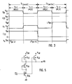
- F ig. 5 shows an example of a circuit of the voltage generator 25.
- a P-channel MIS transistor Q 31 , an N-channel depletion MIS transistor Q 33 and an N-channel MIS transistors are connected in series between the write power voltage Vpp and the ground potential.
- a P-channel MIS transistor Q 32 is connected in parallel with the transistor. Q 32 .
- a control signal C 22 of the opposite phase with respect to the control signal C 22 is applied to the gates of the transistors Q 32 and Q 34 .
- the transistor Q 24 of the circuit takes a conductive state in a write state and a non-conductive state in a read state in response to the value of V 0 .
- Fig. 3 shows waveforms in operations of the memory shown in Figs. 3 and 5.
- T 1 shows a shows a read period in which a period T 1-1 shows the case where the memory cell transistor M 21 is not selected.
- the row decoder signal D 21 is at high to make the transistor Q 22 conductive.
- the potential. C 21 is kept at V CC throught the whole operation. While the control signal C 22 and the voltage V 0 are approximately at Vpp so that the transistors Q 24 and Q 25 are non-conductive. Accordingly, the word line X 2 is at low in level.
- a period T 1-2 shows the case where the cell transistor M 21 is selected in a read cycle.
- the row decoder signal D 21 is the ground potential and the transistor Q 21 is conducting. While the transistors Q 24 and Q 25 are still non-condueting. Therefore, the word line X 2 is raised in potential close to V CC via the transistors Q 21 and Q 23 , while the digit line B 21 , is connected to the node N 2 via the circuit 24, and the switch SW.
- a write cycle is shown as T 2 .
- a period T 2-1 shows the case where the cell transistor is not selected.
- the control signal C 22 is approximately at the ground potential and the voltage V 0 is at the intermediate level.of (Vpp- ⁇ ) so that the transistors Q 24 and Q 25 are conductive.
- the transistor Q 22 is conductive in response to the high level of D 21 . Therefore, the word line X 2 is made approximately at the ground level through Q 22 and Q 23 .
- the transistor Q 24 operates to limit the current flowing therethrough.
- the potential of the word line X 2 is effectively set at the ground potential and the power consumption due to this current.is also reduced.
- a period T 2-2 is the case where the cell transistor M 21 is selected.
- the row decoder signal D 21 is at the low level to make the transistor Q 22 non-conductive and the transistor Q 21 conductive. Therefore, the potential of the word line is raised to Vpp via the transistors Q 24 and Q 25 , achieving the selection of the word line X 2 .
- Vpp is also applied to the drain of M 21 via the circuit 24 and the switch SW.
- F ig. 4 shows a practical. layout where a plurality of memory cell transistors are arranged in a matrix form. In Fig. 4, the portions corresponding to those in Fig. 2 are designated by similar references.
- Each consecutive four word lines, e.g. X 11 to X 14 and their word driving schemes are classified into blocks BL l to BL m .
- Each of the'blocks BL l to SL m has the same structure and the block BL l is representatively illustrated.
- Main row decoders RD1 to RD m receiving row address signals a 0 to a i , a 0 to a i provided for the blocks BL l to BL m .
- Each of the main row decoders RD l to RD m selects its corresponding block, e.g. BL l .
- the low level of the output D 1 of the decoder RD 1 selects the block BL l .
- a NOR type row address driver 21'-1 receives the output Di and a sub row decoded signal AX 1 and select the word line when both of D 1 and AXi are low.
- Other row address drivers 21'-2 to 21'-4 have the same structure as 21'-1 except different sub row decoded signals AX 2 , AX 3 and AX 4 are applied.
- the signals AX 1 to AX 4 are the signals obtained by decoding two bits.of row address signals which are not applied to the decoders RD l to RD m .
- the write voltage apply circuit 23'-1 to 23'-4 are connected between the write voltage Vpp and the word lines X 11 to X 14 in the block BL l .
- the signal C 22 and the voltage V o are applied to all the write voltage circuits in common.
- column selection scheme such as the circuits 24, switch SW, the transistor Q 26 and the amplifier 25 in Fig. 2 is provided in a known way.
- a non-volatile semiconductor memory having a high density structure can be fabricated without using depletion MIS transistors.
Landscapes
- Read Only Memory (AREA)
Applications Claiming Priority (2)
| Application Number | Priority Date | Filing Date | Title |
|---|---|---|---|
| JP277434/84 | 1984-12-28 | ||
| JP27743484 | 1984-12-28 |
Publications (3)
| Publication Number | Publication Date |
|---|---|
| EP0186907A2 true EP0186907A2 (de) | 1986-07-09 |
| EP0186907A3 EP0186907A3 (en) | 1988-04-20 |
| EP0186907B1 EP0186907B1 (de) | 1991-10-09 |
Family
ID=17583505
Family Applications (1)
| Application Number | Title | Priority Date | Filing Date |
|---|---|---|---|
| EP85116578A Expired - Lifetime EP0186907B1 (de) | 1984-12-28 | 1985-12-27 | Nichtflüchtige Halbleiterspeicheranordnung mit Schreibeschaltung |
Country Status (4)
| Country | Link |
|---|---|
| US (1) | US4710900A (de) |
| EP (1) | EP0186907B1 (de) |
| JP (1) | JPH0746515B2 (de) |
| DE (1) | DE3584362D1 (de) |
Families Citing this family (25)
| Publication number | Priority date | Publication date | Assignee | Title |
|---|---|---|---|---|
| IT1214607B (it) * | 1985-05-14 | 1990-01-18 | Ates Componenti Elettron | Circuito di precarica per linee di riga di un sistema di memoria, in particolare a celle programmabili. |
| US5050124A (en) * | 1986-09-30 | 1991-09-17 | Kabushiki Kaisha Toshiba | Semiconductor memory having load transistor circuit |
| FR2605447B1 (fr) * | 1986-10-20 | 1988-12-09 | Eurotechnique Sa | Memoire non volatile programmable electriquement |
| FR2606199B1 (fr) * | 1986-11-04 | 1988-12-09 | Eurotechnique Sa | Circuit integre du type circuit logique comportant une memoire non volatile programmable electriquement |
| JP2589076B2 (ja) * | 1987-01-14 | 1997-03-12 | 日本テキサス・インスツルメンツ株式会社 | 記憶装置 |
| FR2609831B1 (fr) * | 1987-01-16 | 1989-03-31 | Thomson Semiconducteurs | Circuit de lecture pour memoire |
| JPH0777078B2 (ja) * | 1987-01-31 | 1995-08-16 | 株式会社東芝 | 不揮発性半導体メモリ |
| JPH0772996B2 (ja) * | 1987-01-31 | 1995-08-02 | 株式会社東芝 | 不揮発性半導体メモリ |
| JPS63251999A (ja) * | 1987-04-08 | 1988-10-19 | Mitsubishi Electric Corp | 半導体記憶装置 |
| US4885719A (en) * | 1987-08-19 | 1989-12-05 | Ict International Cmos Technology, Inc. | Improved logic cell array using CMOS E2 PROM cells |
| JPH081759B2 (ja) * | 1987-11-24 | 1996-01-10 | 株式会社東芝 | 不揮発性メモリ |
| US4858186A (en) * | 1988-01-12 | 1989-08-15 | Intle Corporation | A circuit for providing a load for the charging of an EPROM cell |
| US4820941A (en) * | 1988-02-01 | 1989-04-11 | Texas Instruments Incorporated | Decoder driver circuit for programming high-capacitance lines |
| IT1228166B (it) * | 1988-10-06 | 1991-05-31 | Sgs Thomson Microelectronics | Circuito programmabile di selezione statica per dispositivi programmabili |
| JPH0821849B2 (ja) * | 1988-10-25 | 1996-03-04 | 富士通株式会社 | 半導体記憶装置 |
| US5027320A (en) * | 1989-09-22 | 1991-06-25 | Cypress Semiconductor Corp. | EPROM circuit having enhanced programmability and improved speed and reliability |
| JPH03179780A (ja) * | 1989-12-07 | 1991-08-05 | Fujitsu Ltd | 半導体装置 |
| US5481492A (en) * | 1994-12-14 | 1996-01-02 | The United States Of America As Represented By The Secretary Of The Navy | Floating gate injection voltage regulator |
| JP3159359B2 (ja) * | 1995-06-22 | 2001-04-23 | 日本電気株式会社 | 半導体装置 |
| US5673218A (en) | 1996-03-05 | 1997-09-30 | Shepard; Daniel R. | Dual-addressed rectifier storage device |
| US6956757B2 (en) | 2000-06-22 | 2005-10-18 | Contour Semiconductor, Inc. | Low cost high density rectifier matrix memory |
| EP1892724B1 (de) | 2006-08-24 | 2009-12-09 | STMicroelectronics S.r.l. | Speichervorrichtung mit einem Zeilenselektor mit in Serie geschalteten Mittelspannungstransistoren |
| US7512029B2 (en) * | 2006-06-09 | 2009-03-31 | Micron Technology, Inc. | Method and apparatus for managing behavior of memory devices |
| US7813157B2 (en) * | 2007-10-29 | 2010-10-12 | Contour Semiconductor, Inc. | Non-linear conductor memory |
| US8325556B2 (en) | 2008-10-07 | 2012-12-04 | Contour Semiconductor, Inc. | Sequencing decoder circuit |
Citations (3)
| Publication number | Priority date | Publication date | Assignee | Title |
|---|---|---|---|---|
| GB2094086A (en) * | 1981-03-03 | 1982-09-08 | Tokyo Shibaura Electric Co | Non-volatile semiconductor memory system |
| EP0088912A2 (de) * | 1982-03-15 | 1983-09-21 | Texas Instruments Incorporated | Subschwellenwert-Lastelement für statische RAM-Zelle |
| US4446536A (en) * | 1982-06-21 | 1984-05-01 | Mcdonnell Douglas Corporation | Complementary metal oxide semiconductors address drive circuit |
Family Cites Families (2)
| Publication number | Priority date | Publication date | Assignee | Title |
|---|---|---|---|---|
| JPS5952497A (ja) * | 1982-09-17 | 1984-03-27 | Nec Corp | デコ−ダ回路 |
| US4565932A (en) * | 1983-12-29 | 1986-01-21 | Motorola, Inc. | High voltage circuit for use in programming memory circuits (EEPROMs) |
-
1985
- 1985-12-25 JP JP29427185A patent/JPH0746515B2/ja not_active Expired - Lifetime
- 1985-12-27 DE DE8585116578T patent/DE3584362D1/de not_active Expired - Fee Related
- 1985-12-27 EP EP85116578A patent/EP0186907B1/de not_active Expired - Lifetime
- 1985-12-30 US US06/814,472 patent/US4710900A/en not_active Expired - Lifetime
Patent Citations (3)
| Publication number | Priority date | Publication date | Assignee | Title |
|---|---|---|---|---|
| GB2094086A (en) * | 1981-03-03 | 1982-09-08 | Tokyo Shibaura Electric Co | Non-volatile semiconductor memory system |
| EP0088912A2 (de) * | 1982-03-15 | 1983-09-21 | Texas Instruments Incorporated | Subschwellenwert-Lastelement für statische RAM-Zelle |
| US4446536A (en) * | 1982-06-21 | 1984-05-01 | Mcdonnell Douglas Corporation | Complementary metal oxide semiconductors address drive circuit |
Also Published As
| Publication number | Publication date |
|---|---|
| EP0186907A3 (en) | 1988-04-20 |
| EP0186907B1 (de) | 1991-10-09 |
| JPS61267996A (ja) | 1986-11-27 |
| US4710900A (en) | 1987-12-01 |
| DE3584362D1 (de) | 1991-11-14 |
| JPH0746515B2 (ja) | 1995-05-17 |
Similar Documents
| Publication | Publication Date | Title |
|---|---|---|
| US4710900A (en) | Non-volatile semiconductor memory device having an improved write circuit | |
| US5596525A (en) | Memory cell of nonvolatile semiconductor memory device | |
| EP0551926B1 (de) | Nichtflüchtige Halbleiter-Speicheranordnung | |
| US5394372A (en) | Semiconductor memory device having charge-pump system with improved oscillation means | |
| US5270969A (en) | Electrically programmable nonvolatile semiconductor memory device with nand cell structure | |
| US5740107A (en) | Nonvolatile integrated circuit memories having separate read/write paths | |
| US4761764A (en) | Programmable read only memory operable with reduced programming power consumption | |
| US6233198B1 (en) | High density flash memory device with improved row decoding structure | |
| EP0052566A2 (de) | Elektrisch löschbarer, programmierbarer Festwertspeicher | |
| KR930703518A (ko) | 소거특성을 개량한 플래쉬메모리 및 그것에 대한 회로 | |
| JPH0143400B2 (de) | ||
| US6515911B2 (en) | Circuit structure for providing a hierarchical decoding in semiconductor memory devices | |
| KR950000029B1 (ko) | 기생용량에 의해 야기된 오동작을 방지하기 위한 eprom의 디코더 회로 | |
| EP0078502B1 (de) | Speicherschaltung | |
| JPH0762960B2 (ja) | 半導体回路 | |
| US5978263A (en) | Negative voltage switch architecture for a nonvolatile memory | |
| KR100254565B1 (ko) | 분할된 워드 라인 구조를 갖는 플래시 메모리 장치의 행 디코더회로 | |
| US3702926A (en) | Fet decode circuit | |
| KR100490605B1 (ko) | 비휘발성 반도체기억장치 | |
| US5719805A (en) | Electrically programmable non-volatile semiconductor memory including series connected memory cells and decoder circuitry for applying a ground voltage to non-selected circuit units | |
| US6034899A (en) | Memory cell of nonvolatile semiconductor memory device | |
| US6272045B1 (en) | Nonvolatile semiconductor memory device | |
| US5877981A (en) | Nonvolatile semiconductor memory device having a matrix of memory cells | |
| EP0365721B1 (de) | Programmierbarer Halbleiterspeicher | |
| JPH05243531A (ja) | 不揮発性記憶装置 |
Legal Events
| Date | Code | Title | Description |
|---|---|---|---|
| PUAI | Public reference made under article 153(3) epc to a published international application that has entered the european phase |
Free format text: ORIGINAL CODE: 0009012 |
|
| 17P | Request for examination filed |
Effective date: 19851227 |
|
| AK | Designated contracting states |
Kind code of ref document: A2 Designated state(s): DE FR GB |
|
| PUAL | Search report despatched |
Free format text: ORIGINAL CODE: 0009013 |
|
| AK | Designated contracting states |
Kind code of ref document: A3 Designated state(s): DE FR GB |
|
| 17Q | First examination report despatched |
Effective date: 19900402 |
|
| GRAA | (expected) grant |
Free format text: ORIGINAL CODE: 0009210 |
|
| AK | Designated contracting states |
Kind code of ref document: B1 Designated state(s): DE FR GB |
|
| REF | Corresponds to: |
Ref document number: 3584362 Country of ref document: DE Date of ref document: 19911114 |
|
| ET | Fr: translation filed | ||
| PLBE | No opposition filed within time limit |
Free format text: ORIGINAL CODE: 0009261 |
|
| STAA | Information on the status of an ep patent application or granted ep patent |
Free format text: STATUS: NO OPPOSITION FILED WITHIN TIME LIMIT |
|
| 26N | No opposition filed | ||
| PGFP | Annual fee paid to national office [announced via postgrant information from national office to epo] |
Ref country code: FR Payment date: 20011212 Year of fee payment: 17 |
|
| PGFP | Annual fee paid to national office [announced via postgrant information from national office to epo] |
Ref country code: GB Payment date: 20011227 Year of fee payment: 17 |
|
| REG | Reference to a national code |
Ref country code: GB Ref legal event code: IF02 |
|
| PGFP | Annual fee paid to national office [announced via postgrant information from national office to epo] |
Ref country code: DE Payment date: 20020109 Year of fee payment: 17 |
|
| PG25 | Lapsed in a contracting state [announced via postgrant information from national office to epo] |
Ref country code: GB Free format text: LAPSE BECAUSE OF NON-PAYMENT OF DUE FEES Effective date: 20021227 |
|
| PG25 | Lapsed in a contracting state [announced via postgrant information from national office to epo] |
Ref country code: DE Free format text: LAPSE BECAUSE OF NON-PAYMENT OF DUE FEES Effective date: 20030701 |
|
| GBPC | Gb: european patent ceased through non-payment of renewal fee |
Effective date: 20021227 |
|
| PG25 | Lapsed in a contracting state [announced via postgrant information from national office to epo] |
Ref country code: FR Free format text: LAPSE BECAUSE OF NON-PAYMENT OF DUE FEES Effective date: 20030901 |
|
| REG | Reference to a national code |
Ref country code: FR Ref legal event code: ST |