EP0347935A2 - Dispositif de mémoire semi-conductrice - Google Patents
Dispositif de mémoire semi-conductrice Download PDFInfo
- Publication number
- EP0347935A2 EP0347935A2 EP89111475A EP89111475A EP0347935A2 EP 0347935 A2 EP0347935 A2 EP 0347935A2 EP 89111475 A EP89111475 A EP 89111475A EP 89111475 A EP89111475 A EP 89111475A EP 0347935 A2 EP0347935 A2 EP 0347935A2
- Authority
- EP
- European Patent Office
- Prior art keywords
- potential
- load
- dummy
- gate
- memory device
- Prior art date
- Legal status (The legal status is an assumption and is not a legal conclusion. Google has not performed a legal analysis and makes no representation as to the accuracy of the status listed.)
- Granted
Links
- 239000004065 semiconductor Substances 0.000 title claims abstract description 77
- 238000005513 bias potential Methods 0.000 claims description 16
- 230000008859 change Effects 0.000 claims description 7
- 230000001419 dependent effect Effects 0.000 claims description 2
- 230000004044 response Effects 0.000 claims 4
- 239000000872 buffer Substances 0.000 description 19
- 108091006146 Channels Proteins 0.000 description 10
- 230000003334 potential effect Effects 0.000 description 10
- 238000010586 diagram Methods 0.000 description 9
- 230000007257 malfunction Effects 0.000 description 9
- 230000001052 transient effect Effects 0.000 description 9
- 230000007423 decrease Effects 0.000 description 5
- 230000000694 effects Effects 0.000 description 3
- 230000004048 modification Effects 0.000 description 3
- 238000012986 modification Methods 0.000 description 3
- 239000003990 capacitor Substances 0.000 description 2
- 238000007599 discharging Methods 0.000 description 2
- 229910021420 polycrystalline silicon Inorganic materials 0.000 description 2
- 229920005591 polysilicon Polymers 0.000 description 2
- 239000000758 substrate Substances 0.000 description 2
- 230000007704 transition Effects 0.000 description 2
- WQJQOUPTWCFRMM-UHFFFAOYSA-N tungsten disilicide Chemical compound [Si]#[W]#[Si] WQJQOUPTWCFRMM-UHFFFAOYSA-N 0.000 description 2
- 229910021342 tungsten silicide Inorganic materials 0.000 description 2
- 230000002730 additional effect Effects 0.000 description 1
- 230000003321 amplification Effects 0.000 description 1
- 238000013459 approach Methods 0.000 description 1
- 230000003247 decreasing effect Effects 0.000 description 1
- 230000006870 function Effects 0.000 description 1
- 230000006872 improvement Effects 0.000 description 1
- 239000012535 impurity Substances 0.000 description 1
- 238000004519 manufacturing process Methods 0.000 description 1
- 239000000463 material Substances 0.000 description 1
- 239000011159 matrix material Substances 0.000 description 1
- 238000003199 nucleic acid amplification method Methods 0.000 description 1
- 230000000717 retained effect Effects 0.000 description 1
- 230000000630 rising effect Effects 0.000 description 1
Images


Classifications
-
- G—PHYSICS
- G11—INFORMATION STORAGE
- G11C—STATIC STORES
- G11C7/00—Arrangements for writing information into, or reading information out from, a digital store
-
- G—PHYSICS
- G11—INFORMATION STORAGE
- G11C—STATIC STORES
- G11C7/00—Arrangements for writing information into, or reading information out from, a digital store
- G11C7/12—Bit line control circuits, e.g. drivers, boosters, pull-up circuits, pull-down circuits, precharging circuits, equalising circuits, for bit lines
-
- G—PHYSICS
- G11—INFORMATION STORAGE
- G11C—STATIC STORES
- G11C16/00—Erasable programmable read-only memories
- G11C16/02—Erasable programmable read-only memories electrically programmable
- G11C16/06—Auxiliary circuits, e.g. for writing into memory
- G11C16/26—Sensing or reading circuits; Data output circuits
- G11C16/28—Sensing or reading circuits; Data output circuits using differential sensing or reference cells, e.g. dummy cells
-
- G—PHYSICS
- G11—INFORMATION STORAGE
- G11C—STATIC STORES
- G11C7/00—Arrangements for writing information into, or reading information out from, a digital store
- G11C7/06—Sense amplifiers; Associated circuits, e.g. timing or triggering circuits
- G11C7/062—Differential amplifiers of non-latching type, e.g. comparators, long-tailed pairs
-
- G—PHYSICS
- G11—INFORMATION STORAGE
- G11C—STATIC STORES
- G11C7/00—Arrangements for writing information into, or reading information out from, a digital store
- G11C7/14—Dummy cell management; Sense reference voltage generators
Definitions
- the present invention relates to a semiconductor memory device improved in a reference potential generating circuit for a sense amplifier and load circuits for memory cells.
- a conventional semiconductor memory device shown in Fig. 1 is an erasable and programmable ROM (EPROM) using floating gate MOSFETs as memory cells.
- EPROM erasable and programmable ROM
- MC11, MC12, ..., MC1n designate floating gate MOSFETs; DC a floating gate MOSFET as a dummy cell; WL1, WL2, ..., WLm row lines; BL1, BL2, ..., BLn column lines; DBL a dummy column line; 11 a row decoder; 12 a column decoder; BT1, BT2, .., BTn column gate MOSFETs for column selection; DBT a MOSFET that is equivalent to the column gate MOSFET and is normally in a conductive state with application of a power voltage Vcc to the gate of the MOSFET; 13A a first bias setting circuit made up of n-channel MOSFETs QM1 to QM6; 14A a first load circuit made up of a p-channel MOSFET QM7; 13B a second bias setting circuit made up of n-channel MOSFETs QD1 to QD6; 14B a second load circuit made up of
- MOSFETs whose channels are not specified will be treated as n-channel MOSFETs.
- the dummy cell DC consists of a MOSFET equivalent to that of a memory cell MC that is any of the memory cells MC11 to MCmn.
- the dummy column line DBL is equivalent to the column line BL that is any of those column lines BL1 to BLn.
- the node potential V2 is set at a voltage which is the sum of a potential on the column line BL when a predetermined current flows into the memory cell MC, and a threshold voltage of the n-channel MOSFET containing an increased threshold voltage due to the substrate bias effect.
- the MOSFET QM4 is an initial charging MOSFET for quickening an initial charging to the column line BL in which the column line BL is charged from an initial voltage 0 V.
- the initial charging MOSFET is rendered nonconductive when the column line potential exceeds a potential on the column line when a predetermined current flows into the memory cell MC.
- a reference potential Vref is generated by the second load circuit 14B on the basis of the data in the dummy cell DC, and appears at a node B.
- An input potential Vin is generated by the first load circuit 14A on the basis of the data read out of a memory cell MC as selected by the output signals of the row decoder 11 and the column decoder 12, and appears at a node A.
- the sense amplifier 15 compares the reference potential Vref and the input potential Vin to sense a type of the data stored in the memory cell MC.
- the sensed data is amplified by the sense amplifier 15, and outputted through the output buffer 16.
- each memory cell of the EPROM data is programmed by selectively injecting electrons into the floating gate of the cell.
- a high voltage e.g., 12.5 to 21 V, which is much higher than the normal power voltage, e.g., 5 V
- the normal power voltage e.g. 5 V
- an impact ionization occurs in the vicinity of the drain of the memory cell located at a cross point of the selected row and column lines, to generate electron-hole pairs.
- the electrons are injected into the floating gate of the memory cell.
- a threshold voltage of the memory cell injected with electrons is much higher than that of the memory cell not injected.
- the memory cell whose floating gate is injected with electrons maintains an off-state even if a signal of "1" level (power voltage Vcc) is supplied to the control gate of the cell, or the row line. Under the same condition, the memory cell not injected with electrons is turned on. Since the dummy cell DC is not injected with electrons, no potential difference is caused between the potentials Vref and Vin.
- a channel width WD7 of the MOSFET QD7 in the second load circuit 14B is set to be larger than that WM7 of the MOSFET QM7 in the first load circuit 14A.
- a conduction resistance of the MOSFET QD7 is smaller than that of the MOSFET QM7.
- the conduction resistance of the MOSFET QD7 is so selected that the reference potential Vref is between the Vin potential when the electron injected memory cell is selected and the Vin potential when the no electron injected memory cell is selected.
- the potential Vin represents a potential which is the result of a subtraction of the threshold voltage of the load MOSFET QM7 from the power source voltage Vcc.
- the electron injected memory cell or the memory cell with a high threshold level will be assumed to be a memory cell storing "0" data.
- the no electron injected memory cell or the memory cell with a low threshold voltage will be assumed to be a memory cell storing "1" data.
- the EPROM of Fig. 1 will encounter a situation that a row line connected to the memory cells of "1" data that is currently selected is switched to another row line connected to the memory cell having the same data, and subsequently the data are successively read out from the memory cells on the new row.
- the memory cells selected anew are insufficiently turned on in the initial stage, until the potential of the row line selected anew reaches power source voltage Vcc. Consequently, the potential of the selected bit line is temporarily increased.
- the threshold voltage of the memory cell of the floating gate structure is approximately 2 V.
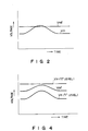
- the reference potential Vref is always constant as shown in Fig. 2 showing waveforms of potentials Vref and Vin.
- the sense amplifier 15 tem When the potential Vin rises and crosses a line of the reference potential Vref as shown, the sense amplifier 15 temporarily produces the data of an improper logic level.
- the output data of the buffer 16 varies its logic level, "1" ⁇ "0" ⁇ "1", during a short period. Therefore, an inductance component existing in the lead creates a great variation of the earth voltage, possibly causing a malfunction of a circuit in the EPROM.
- the dummy cells DC1 to DCm are provided corresponding to row lines WL1 to WLm, respectively.
- the control gates of the dummy cells DC1 to DCm are connected to the row lines WL1 to WLm, respectively.
- the drains of the dummy cells DC1 to DCm are connected to a dummy column line DBL.
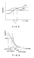
- a characteristic curve depicted by a solid line in Fig. 6 shows a voltage vs. current characteristic curve of the first load circuit 14A in the conventional semiconductor memory device.
- the abscissa represents a potential Vin at the node A and the ordinates a load current flowing into the load circuit. It is assumed that Vin ("1" level) is a potential at the node A caused when the memory cell of a low threshold voltage is selected and a memory cell current Icell flows, and Vin (“0" level) is a potential at the node A and Vref is a potential at the node B.
- the column line is switched one from the other, and the memory cell of a high threshold voltage is selected, the charging to the new selected column line starts at the voltage of 0 V. Accordingly, capacitance connected to the column lines has become large, with the increase of the semiconductor memory capacity. Accordingly, to realize a high speed read operation, it is necessary to quicken both the charging speed of the column line and the read operation for reading out the "0" data.
- the column line is charged at a high speed through the initial charging transistor QM4 when the potential is less than Vin ("1" level). When the potential of the column line BL exceeds Vin ("1" level), the transistor QM4 becomes nonconductive.
- the p-channel transistor QM7 in the load circuit 14A charges the column line BL. Since the gate of the p-channel transistor QM7 is connected to the drain thereof, when the potential Vin at the node A rises, a conduction resistance of this transistor QM7 rapidly increases, and a charge current rapidly decreases. Therefore, it takes much time for the potential at the node A to rise from Vin ("1" level) to Vin ("0" level), lowering the data read speed. In other words, the time taken for the node A potential to rise from Vin ("1" level) to Vin (“0" level) can be reduced by increasing the the channel width of the transistor QM7 and reducing its conduction resistance. However, the decrease of the conduction resistance of the transistor QM7 creates another problem that a margin for the power source noise is narrowed.
- an object of the present invention is to provide a semiconductor memory device which is free from the power noise even during a transient period that row lines are switched from one to the other, and is operable at an increased data read speed.
- a semiconductor memory device comprising: row lines; memory cells selected by the row lines; column lines receiving data from the memory cells; a first load circuit coupled with the column lines; first dummy cells selected by the row lines; a dummy column line to which the first dummy cells are connected; a second load circuit connected to the dummy column line; a pulse signal generating circuit for generating a pulse signal by detecting a change in an address input signal; a second dummy cell connected to the dummy column line and controlled in conduction by a pulse signal generated by the pulse signal generating circuit; and a sense amplifier for sensing the data stored in the memory cell in accordance with a potential difference between the column line and the dummy column line.
- a semiconductor memory device comprising: row lines; memory cells selected by the row lines; column lines receiving data from the memory cells; a first load circuit coupled with the column lines; first dummy cells selected by the row lines; a dummy column line to which the first dummy cells are connected; a pulse signal generating circuit for generating a pulse signal by detecting a change in an address input signal; a second load circuit connected to the dummy column line, a conduction resistance of the second load circuit to the dummy column line being controlled by a pulse signal generated by the pulse signal generating circuit; and a sense amplifier for sensing the data stored in the memory cell in accordance with a potential difference between the column line and the dummy column line.
- a semiconductor memory device which has a large operation margin against a variation of a power voltage due to power source noise, and can easily realize a high operation speed.
- a semiconductor memory device comprising: at least one memory cell; a first MOS transistor connected at one end of the source-drain current path to the drain of the memory cell and at the other end of the source-drain current path to a data sensing node, and the first MOS transistor receiving at the gate a first bias voltage; a load circuit including a first load means and a second load means that are connected in series, the first load means being inserted between the data sensing node and a first power source, when the memory cell is conductive, the first load means operating as a current limiting load, the second load means lowering a potential at the data sensing node below a potential of the first power source when the memory cell is nonconductive, in the load circuit, a conduction resistance of the first load means being larger than a conduction resistance of the second load means; and a sense circuit for reading out the data from the memory cell.
- the amount of the current flowing through the lead circuit is determined mainly by the first load means in the load circuit.
- a conduction resistance in the load circuit is determined mainly by a conduction resistance in the first load means.
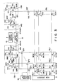
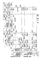
- FIG. 7 there is shown a circuit diagram of a circuit arrangement for data-sensing of an EPROM using floating gate MOSFETs as already mentioned in the prior art description, to which a semiconductor memory device according to the present invention is applied.
- the dummy cell DC that is any one of the dummy cells DC1 to DCm comprises a MOSFET equivalent to that of a memory cell MC that is any one of the memory cells MC11 to MCmn.
- the dummy cell DCm+1 also comprises a MOSFET equivalent to that of the memory cell MC.
- the drains of them are connected together to the dummy column line DBL.
- the control gates of them are connected to the row lines WL1 to WLm, respectively.
- the sources of those transistors are grounded.
- the drain of the dummy cell DCm+1 is connected to the dummy column line DBL.
- a power voltage Vcc is always supplied to the control gate of the dummy cell DCm+1. The source thereof is grounded.
- the first and second bias potential setting circuit 13A and 13B are constructed like those in the conventional semiconductor memory device.
- the source-drain currnet path of the MOSFET QM1 is inserted between a connection point of the column gate MOSFETs BT1 to BTn and the node A.
- the gate of the MOSFET QM1 is applied with a DC bias potential V1 which is lower than the power voltage Vcc and formed by the two MOSFETs QM2 and QM3.
- the source-drain current path of the MOSFET QM4 is inserted between a connection point of the column gate MOSFETs BT1 to BTn and the power voltage Vcc.
- the gate of the MOSFET QM4 is applied with a DC bias potential V2 which is lower than the DC bias potential V1 and formed by the two MOSFETs QM5 and QM6.
- the DC bias potential V2 is set at a value which is the sum of a column line potential when a memory cell whose threshold voltage is set at a low voltage is selected and a predetermined current flows through the source-drain current path of the memory cell, and a threshold voltage of the n-channel MOSFET containing an increased threshold voltage due to a substrate bias effect.
- the circuit arrangement of the second bias potential setting circuit 13B is substantially the same as that of the first bias potential setting circuit when the MOSFETs QD1 to QD6 are replaced by the MOSFETs QM1 to QM6.
- the first and second load circuits 14A and 14B are also substantially the same as those in the conventional memory device.
- the source-drain current path of MOSFET QM7 is inserted between the node A and the power source Vcc.
- the gate of the MOSFET QM7 is connected to its drain and the node A.
- the MOSFET QM4 in the first bias potential setting circuit 13A is for the initial charging of the column line.
- the DC bias voltage V2 is set such that the MOSFET QM4 is turned off when the column line potential exceeds a column potential when a predetermined current flows into the memory cell.
- the circuit arrangement of the second load circuit 14B is substantially the same as that in the conventional memory device. However, the conduction resistance is set larger than that in the conventional device.
- the dummy column line DBL is connected to the dummy cell DCm+1, which constantly receives at the gate the power voltage Vcc, and normally in an on state. And, the dummy column line DBL is discharged through the dummy cell DCm+1 and a dummy cell DC (indicates any one of the dummy cells DC1 to DCm) connected to the selected row line WL.
- the conduction resistance of the load MOSFET QD7 in the second load circuit 14B is set to be approximately two times that of the MOSFET QD7 in the conventional memory device shown in Fig. 1.
- memory cells storing "1" data that are selected by switching one row line to other row line are successively subjected to a data read operation.
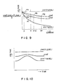
- the current flowing through the dummy cell at the time of this row line switching is shown by a curve of a solid line in Fig. 8B.
- the value "x" of the current equals to the current flowing through the selected dummy cell DC when the potential of the selected row line is the power source voltage Vcc.
- the dummy cell is formed of a floating gate type MOS transistor which is the same in structure, channel width, and channel length as that of the memory cell in the memory matrix.
- the current flowing through the memory cell whose control gate is continuously supplied with the power source Vcc equals to the value "x". Consequently, the current flowing through the dummy cell DCm+1 also becomes the value "x" and thus, the current flowing through the dummy cell before the row lines are switched becomes "2x".
- Fig. 9 shows a variation of the reference potential Vref (indicated by a solid line) against the sum of the currents flowing through all the dummy cells, which is prepared on the basis of the Fig. 8 data.
- the illustration of Fig. 9 contains potential variations of an input potential Vin ("1" level) when the data is read out from the memory cell storing "1" data against the sum of the currents flowing through all the dummy cells, an input potential Vin ("0" level) when the data is read out from the memory cell storing "0" data, and a reference potential Vref in the conventional memory device of Fig. 1 (indicated by a one-dot-chain line) against the current flowing through the dummy cell.
- the input potential Vin ("0" level) is constant since no current flows through the dummy cells when "0" data is read out.
- the dummy column line DBL is connected to the dummy cell DC driven by the selected row line and the dummy cell DCm+1 driven by power source Vcc. Because of this, the conduction resistance of the MOSFET QD7 in the second load circuit 14B is selected such that when a double cell current flows, the same reference potential as that of the conventional memory device can be obtained.
- the current flowing through the dummy cell becomes minimum (a point where the current is "y") at the time of the row line switching.
- the reference potential Vref rises to the potential at point P4 in the conventional memory device of Fig. 1.
- the reference potential Vref rises to reach just the potential at point P5, since the current flowing through the dummy cells is "x + y".
- Fig. 10 there are shown variations of the reference potentials Vref and the input potential Vin when the row lines are switched and the memory cells storing "1" data on the new row line is subjected to the data read operation, subsequent to the memory cells on the previous row line.
- the degree of the increase of a potential level of the reference potential Vref is much lower when compared with the degree of the increase of the reference voltage Vref in the conventional memory device of Fig. 3 (see Fig. 4).
- the curve of the reference potential Vref never crosses the line of the input potential Vin in the memory device. Therefore, the occurrence of the power source noise due to the operation of the output buffer is prevented.
- the reading speed is higher than that of the conventional device by such an amount of time T2 (Fig. 11) that a rising speed of the reference potential (indicated by a one-dot-chain line) in the present embodiment is lower than that of the reference potential (indicated by a broken line) in the conventional semiconductor device. This contributes to improvement of the data read speed.
- the power voltage Vcc is applied to the gate of the dummy cell DCm+1 for adjusting the reference potential, but it may be any other voltage than the voltage Vcc, provided that it is constant when the row lines are switched.
- the dummy cells DC1 to DCm and the dummy cell DCm+1 are connected to the same dummy column line DBL.
- Two different dummy column lines may be provided and be connected to the dummy cells DC1 to DCm, and the dummy cell DCm+1, respectively.
- each dummy column line is coupled with a MOSFET equivalent to the column gate MOSFET, and a load circuit.
- the load circuits coupled with these dummy column lines produce output signals which are supplied to an input of the sense amplifier 15.
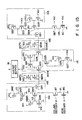
- FIG. 12 Another embodiment of a semiconductor memory device according to the present invention will be described with reference to Fig. 12. Also in this embodiment, the present invention is applied into an EPROM using floating gate MOSFETs as memory cells.
- the present embodiment is different from the embodiment of Fig. 7 in the following points.
- An address transition detector (ATD) 18 is additionally used. An output signal of the ATD 18 is applied to the gate of the dummy cell DCm+1. In the Fig. 7 embodiment, the power voltage Vcc is constantly applied to the same.
- a row address is applied to the row address buffer 17. When a row address changes and the word lines are switched, the ATD 18 generates a pulse signal of a predetermined pulse width.
- reference numeral 19 designates a column address buffer receiving a column address.
- the output signals of the address buffers 17 and 19 are applied to the row and column decoders 17 and 19, respectively.
- the ATD 18 produces a pulse signal to turn on the dummy cell.
- the dummy cell is turned on during the time of the row line switching. Accordingly, at the time of the row line switching, a current flowing into the dummy column line DBL increases, to hold back a rise of the reference potential Vref.
- the conduction resistance of the load MOSFET QD7 in the second load circuit 14B is set at a value comparable to that of the MOSFET QD7 in the conventional semiconductor device.
- the discharge current of the dummy column line DBL is increased.
- the holding back of the rise of the reference potential Vref may be realized by directly controlling the conduction resistance of the second load circuit 14B, not using the dummy cell DCm+1.
- Fig. 14 shows a timing chart for explaining the operation of the ATD 18 that is used in the embodiments of Figs. 12 and 13.
- a row address signal externally applied changes, and with the change of the address signal, the row line currently used is switched to a new row line.
- the ATD 18 produces a pulse signal which retains a "1" logical state during this period.
- a circuit having such a function may readily be realized by combining signal delay and logic circuits.
- the present invention is applicable not only for the EPROM but also for a mask ROM using MOSFETs of a single gate structure as memory cells, whose threshold voltages are adjusted, low and high, by selectively doping impurity into the channel regions of the transistors during the manufacturing process.
- the p-channel MOSFET for load may be substituted by an n-channel MOSFET if its conduction resistance is comparable to the former. If the n-channel MOSFET is used in the Fig. 13 embodiment, the phase of the pulse signal generated by the ATD 18 must be inverted with respect to that of the pulse signal generated by the ATD in the Fig. 13 embodiment. In the memory device of each of the above embodiments, the dummy cell is not always equivalent to the memory cell.
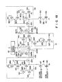
- a couple of p-channel MOSFETs QM7A and QM7B are inserted in series between the power voltage Vcc and the node A.
- a couple of p-channel MOSFETs QD7A and QD7B are connected in series between the power voltage Vcc and the node B.
- the MOS transistors QM7A and QD7A are connected at the gates the node A and B, respectively.
- the gates of the MOS transistors QM7B and QD7B are connected to ground.
- the MOS transistors QM7A and QD7A are designed to have the same sizes.
- the size of each of the transistors QM7A and QD7A is much larger than that of each of the transistors QM7B and QD7B. In other words, the conduction resistance of the former is smaller than that of the latter.
- the transistor QM7B in the first load circuit 14A is so sized as to provide a potential of a "1" level, e.g, 1 V, at node A when a predetermined current flows into the memory cell MC.
- the MOS transistor QM7B when the potential at node A is low, the MOS transistor QM7B dominantly determines a conduction resistance in the load circuit 14A.
- the conduction resistance of the load circuit 14A is dominantly determined by the conduction resistance of the transistor QM7A.
- the sense amplifier 15 is made up of p-channel MOSFETs Q21 and Q22, and n-channel MOSFETs Q23 to Q27.
- the transistors Q21 to Q25 make up a differential amplifier.
- a general differential amplifier may be used for the differential amplifier.
- the transistors Q23 and Q24 make up a differential amplifier.
- the differential amplifier is grounded through the transistor Q25 which receives at the gate a bias potential as generated by the transistors Q26 and Q27.
- Fig. 16 shows a voltage vs. load current characteristic of the load circuit 14A in the embodiment of Fig. 15.
- the abscissa indicates a potential Vin at node A, while the ordinate a current flowing through the load circuit.
- Vin (1" level) denotes a potential at node A when a memory cell storing "1" data is selected and a current Icell flows through the selected memory cell.
- Vin (“0" level) denotes a potential at node A when a memory cell storing "0" data is selected.
- Vref denotes a potential at node B, which is an intermediate potential between the Vin ("1" level) and the Vin ("0" level).
- a solid line indicates the voltage vs. load current characteristic of the load circuit in the semiconductor memory of the Fig. 15 embodiment
- a dotted line indicates the voltage vs. load current characteristic of the load circuit in the conventional semiconductor memory of Fig. 1.
- Fig. 17 shows a potential variation at node A of the embodiment of Fig. 15 when the column lines are switched from one to the other and a memory cell of a high threshold voltage is selected succeeding to a memory cell of a low threshold voltage.
- the potential variation at node A of the conventional memory device of Fig. 1 is indicated by a dotted line. Assume that at time t0, an input address changes, and at time t1, a new column line BL is selected. Until t1, a memory cell of a low threshold voltage is continuously selected. Accordingly, the potential Vin ("1" level) at node A is retained.
- the power voltage varies when the potential difference between nodes A and B is insufficient, and a malfunction will easily occur.
- Fig. 17 if the output of the buffer circuit is switched after ⁇ T has elapsed from when the potential Vin at node A is equal to the potential Vref at node B, the potential Vin at node A is higher by ⁇ V than that of the conventional memory device of Fig. 1. Therefore, even if the output of the buffer circuit is switched after ⁇ T from time t2, the potential Vin at node A in the device of the embodiment is sufficiently high. Therefore, if the power voltage varies due to the output switching of the buffer circuit, a malfunction of the memory device will not occur. This broadens the power noise margin of the semiconductor memory device.
- a semiconductor memory device is capable of reading data in a high speed and has a broad margin for the power noise.
- Fig. 18 shows yet another embodiment of a semiconductor memory device according to the present invention. Also in this embodiment, the present invention is applied to an EPROM using MOSFETs of the double-layer structure containing a floating gate and a control gate.
- MOSFETs of the double-layer structure containing a floating gate and a control gate.
- like reference symbols are used for designating like or equivalent portions in Fig. 15.
- the MOS transistors QM7B and QD7B are turned off. This fact indicates that in a stand-by mode, the power voltage Vcc causes no current, and therefore a power saving is realized.
- the p-channel MOSFET QM7B in Fig.15 is replaced by a depletion type n-channel MOSFET QM8 whose threshold voltage is negative.
- the gate of the transistor QM8 is connected to its source.
- the transistor QM8 like the p-channel MOS transistor QM7B exhibits a substantially constant current load characteristic, and limits a current flowing through the load circuit 19A to provide the similar results to those of the embodiment of Fig. 15.
- a conduction resistance of the MOS transistor QM8 is so selected that when a predetermined current flows into the memory cell, a potential Vin at node A becomes a predetermined potential, e.g., 1 V.
- the load circuit shown in Fig. 19B is featured in that an enhancement type n-channel MOS transistor QM9 with a gate connected to the power voltage Vcc is used in place of the p-channel MOS transistor QM7A, and a depletion type n-channel MOS transistor QM8 having a negative threshold voltage, in place of the p-channel MOS transistor QM7B in the Fig. 15 embodiment.
- the load circuit of Fig. 15B provides such a voltage-current characteristic as shown in Fig. 16, when the conduction resistance of the transistor QM9 is set higher than that of the transistor QM8.
- the conduction resistance of the MOS transistor QM8 is so selected that when a predetermined current flows into the memory cell, a potential Vin at node A becomes a predetermined potential.
- a potential at node A when memory cell of a high threshold voltage is selected is a potential that is by a threshold voltage of the n-channel MOS transistor lower than the power voltage Vcc.
- all of the MOS transistors of the memory device may be of the n-channel. Accordingly, the memory device may be realized by a cheap n-channel MOS integrated circuit.
- a p-channel MOS transistor QM10 is inserted in series between the p-channel MOS transistors QM7A and QM7B in the embodiment of Fig. 15.
- the size of the transistor QM10 is set larger, like the transistor QM7A, than that of the transistor QM7B.
- the gate of the MOS transistor QM1O is connected to the drain.
- a potential at node A when a memory cell of a high threshold voltage is selected is lower than the power voltage Vcc by a voltage of the sum of the threshold voltages of the p-channel MOS transistors QM10 and QM7A.
- Use of the load circuit of Fig. 19C can reduce the amplification level at node A, and realize a high speed operation of the memory device even if the memory device uses a sense amplifier of a low circuit threshold voltage.
- a load circuit whose structure is substantially the same as that of the load circuit shown in Figs. 19A to 19C is used in place of the second load circuit 14B.
- a geometry of the transistor QM8 must be designed so that a potential Vref at node B is at a mid potential between a potential of the "1" level at node A when a predetermined current flows into the memory cell and a potential of the "0" level at node A when no current flows into the memory cell.
- the conduction resistance may be set by applying a proper bias potential to the gate of the current limiting load transistor QM7B, in place of applying the ground potential to the gate.
- the memory cells of the nonvolatile semiconductor memory device of each embodiment as mentioned above are nonvolatile transistors of the double gate structure.
- the present invention is applicable for a mask ROM using the transistors of the single gate structure for the memory cells.
- Figs. 20 and 21 Semiconductor memory devices according to additional embodiments of the present invention are illustrated in Figs. 20 and 21.
- the memory device of Fig. 20 corresponds to the combination of the circuit arrangements of Figs. 15 and 17.
- the dummy column line DBL is connected to a dummy cell DCm+1 connected at the gate to the power voltage Vcc.
- a couple of the MOSFETs QM7A and QM7B are connected in series in the first load circuit 14A, and a couple of the MOSFETs QD7A and QD7B are connected also in series in the second load circuit 14B.
- the memory device of Fig. 21 corresponds to the combination of the circuit arrangements of Figs. 12 and 18.
- the dummy column line DBL is connected to a dummy cell DCm+1 receiving at the gate an output pulse from the ATD 18.
- a couple of the MOSFETs QM7A and QM7B are connected in series in the first load circuit 14A, and a couple of the MOSFETs QD7A and QD7B are connected also in series in the second load circuit 14B.
- any of the load circuits shown in Figs. 19A to 19C is applicable for the memory devices of Figs. 20 and 21.
- a rise of the reference potential Vref is held back even during the transient period of the row line switching, thereby rejecting the enter of power noise into the memory device.
- the data is read out at high speed. Therefore, a broad margin is secured for the power voltage variation.
- the bias circuit of the above structure data reading speed can be enhanced, since the potential Vin at node A greatly changes with regard to a small change of the bit line potential.
- the load circuit 14A is applied to the nonvolatile semiconductor device with the feedback type bias circuit, the operation speed of the semiconductor device can be significantly increased.
- the bias circuits 13A and 13B in the semiconductor circuit of Fig. 7 are replaced by the feedback type bias circuit shown in Fig. 22, it is possible to provide a high-speed nonvolatile semiconductor device which does not malfunction by a power source noise.
Landscapes
- Read Only Memory (AREA)
- Static Random-Access Memory (AREA)
Priority Applications (2)
| Application Number | Priority Date | Filing Date | Title |
|---|---|---|---|
| EP93114324A EP0576046B1 (fr) | 1988-06-24 | 1989-06-23 | Dispositif de mémoire à semi-conducteurs |
| EP93114322A EP0576045B1 (fr) | 1988-06-24 | 1989-06-23 | Dispositif de mémoire à semi-conducteurs |
Applications Claiming Priority (4)
| Application Number | Priority Date | Filing Date | Title |
|---|---|---|---|
| JP156539/88 | 1988-06-24 | ||
| JP15653988A JPH07109719B2 (ja) | 1988-06-24 | 1988-06-24 | 半導体記憶装置 |
| JP161344/88 | 1988-06-29 | ||
| JP16134488A JPH0642320B2 (ja) | 1988-06-29 | 1988-06-29 | 半導体記憶装置 |
Related Child Applications (4)
| Application Number | Title | Priority Date | Filing Date |
|---|---|---|---|
| EP93114324A Division EP0576046B1 (fr) | 1988-06-24 | 1989-06-23 | Dispositif de mémoire à semi-conducteurs |
| EP93114322A Division EP0576045B1 (fr) | 1988-06-24 | 1989-06-23 | Dispositif de mémoire à semi-conducteurs |
| EP93114322.6 Division-Into | 1989-06-23 | ||
| EP93114324.2 Division-Into | 1989-06-23 |
Publications (3)
| Publication Number | Publication Date |
|---|---|
| EP0347935A2 true EP0347935A2 (fr) | 1989-12-27 |
| EP0347935A3 EP0347935A3 (fr) | 1991-05-29 |
| EP0347935B1 EP0347935B1 (fr) | 1995-07-26 |
Family
ID=26484252
Family Applications (3)
| Application Number | Title | Priority Date | Filing Date |
|---|---|---|---|
| EP93114324A Expired - Lifetime EP0576046B1 (fr) | 1988-06-24 | 1989-06-23 | Dispositif de mémoire à semi-conducteurs |
| EP93114322A Expired - Lifetime EP0576045B1 (fr) | 1988-06-24 | 1989-06-23 | Dispositif de mémoire à semi-conducteurs |
| EP89111475A Expired - Lifetime EP0347935B1 (fr) | 1988-06-24 | 1989-06-23 | Dispositif de mémoire semi-conductrice |
Family Applications Before (2)
| Application Number | Title | Priority Date | Filing Date |
|---|---|---|---|
| EP93114324A Expired - Lifetime EP0576046B1 (fr) | 1988-06-24 | 1989-06-23 | Dispositif de mémoire à semi-conducteurs |
| EP93114322A Expired - Lifetime EP0576045B1 (fr) | 1988-06-24 | 1989-06-23 | Dispositif de mémoire à semi-conducteurs |
Country Status (4)
| Country | Link |
|---|---|
| US (1) | US5040148A (fr) |
| EP (3) | EP0576046B1 (fr) |
| KR (1) | KR930001735B1 (fr) |
| DE (3) | DE68926124T2 (fr) |
Cited By (3)
| Publication number | Priority date | Publication date | Assignee | Title |
|---|---|---|---|---|
| EP0443989A3 (en) * | 1990-02-23 | 1992-01-02 | Sgs-Thomson Microelectronics S.R.L. | Sense circuit for reading data stored in nonvolatile memory cells |
| EP0487808A1 (fr) * | 1990-11-19 | 1992-06-03 | STMicroelectronics S.r.l. | Mémoires avec des charges inégales et avec compensation |
| EP1288965A3 (fr) * | 2001-08-31 | 2006-06-21 | Fujitsu Limited | Dispositif de mémoire non-volatile à semiconducteurs |
Families Citing this family (18)
| Publication number | Priority date | Publication date | Assignee | Title |
|---|---|---|---|---|
| US5191552A (en) * | 1988-06-24 | 1993-03-02 | Kabushiki Kaisha Toshiba | Semiconductor memory device with address transition actuated dummy cell |
| US5276643A (en) * | 1988-08-11 | 1994-01-04 | Siemens Aktiengesellschaft | Integrated semiconductor circuit |
| JPH03156795A (ja) * | 1989-11-15 | 1991-07-04 | Toshiba Micro Electron Kk | 半導体メモリ回路装置 |
| KR940005688B1 (ko) * | 1991-09-05 | 1994-06-22 | 삼성전자 주식회사 | 메모리 소자에 있어서 데이터 라인의 프리챠아지 자동 검사 장치 |
| JPH0574181A (ja) * | 1991-09-10 | 1993-03-26 | Nec Corp | 半導体メモリ装置のデータ読み出し回路 |
| JP3397427B2 (ja) * | 1994-02-02 | 2003-04-14 | 株式会社東芝 | 半導体記憶装置 |
| US5390147A (en) | 1994-03-02 | 1995-02-14 | Atmel Corporation | Core organization and sense amplifier having lubricating current, active clamping and buffered sense node for speed enhancement for non-volatile memory |
| DE69424771T2 (de) * | 1994-03-22 | 2000-10-26 | Stmicroelectronics S.R.L., Agrate Brianza | Anordnung zum Lesen einer Speicherzellenmatrix |
| EP0675501B1 (fr) * | 1994-03-31 | 2001-06-13 | STMicroelectronics S.r.l. | Elément de mémoire non-volatile avec cellule programmable double et circuit de lecture correspondant pour circuits de redondance |
| GB9423034D0 (en) * | 1994-11-15 | 1995-01-04 | Sgs Thomson Microelectronics | A reference circuit |
| JPH08221996A (ja) * | 1995-02-17 | 1996-08-30 | Nec Corp | 半導体記憶装置 |
| JP3734550B2 (ja) * | 1996-01-30 | 2006-01-11 | 株式会社ルネサステクノロジ | 半導体記憶装置 |
| EP0798740B1 (fr) * | 1996-03-29 | 2003-11-12 | STMicroelectronics S.r.l. | Système de référence pour déterminer l'état de programmation/non programmation d'une cellule de mémoire, en particulier pour des mémoires non-volatiles |
| US5602788A (en) * | 1996-06-07 | 1997-02-11 | International Business Machines Corporation | Read only memory having localized reference bit lines |
| US5729493A (en) * | 1996-08-23 | 1998-03-17 | Motorola Inc. | Memory suitable for operation at low power supply voltages and sense amplifier therefor |
| EP1063654B1 (fr) * | 1999-06-21 | 2003-03-05 | STMicroelectronics S.r.l. | Procédé de lecture des mémoires avec courant de détéction variable par rapport au tension de lecture, et dispositif pour la réalisation de ce procédé |
| TW559814B (en) * | 2001-05-31 | 2003-11-01 | Semiconductor Energy Lab | Nonvolatile memory and method of driving the same |
| KR100454145B1 (ko) * | 2001-11-23 | 2004-10-26 | 주식회사 하이닉스반도체 | 플래쉬 메모리 장치 |
Family Cites Families (10)
| Publication number | Priority date | Publication date | Assignee | Title |
|---|---|---|---|---|
| JPS53117341A (en) * | 1977-03-24 | 1978-10-13 | Toshiba Corp | Semiconductor memory |
| DE3482724D1 (de) * | 1983-04-07 | 1990-08-23 | Toshiba Kawasaki Kk | Festwertspeicher. |
| JPH0666115B2 (ja) * | 1983-09-26 | 1994-08-24 | 株式会社東芝 | 半導体記憶装置 |
| JPS60150297A (ja) * | 1984-01-13 | 1985-08-07 | Nec Corp | 記憶装置 |
| US4805143A (en) * | 1986-01-16 | 1989-02-14 | Hitachi Ltd. | Read-only memory |
| JPS62197996A (ja) * | 1986-02-24 | 1987-09-01 | Toshiba Corp | 半導体メモリのセンスアンプ |
| JPS62231500A (ja) * | 1986-03-31 | 1987-10-12 | Toshiba Corp | 半導体記憶装置 |
| US4819212A (en) * | 1986-05-31 | 1989-04-04 | Kabushiki Kaisha Toshiba | Nonvolatile semiconductor memory device with readout test circuitry |
| IT1213343B (it) * | 1986-09-12 | 1989-12-20 | Sgs Microelettronica Spa | Circuito di rilevamento dello stato di celle di matrice in memorie eprom in tecnologia mos. |
| JP2507529B2 (ja) * | 1988-03-31 | 1996-06-12 | 株式会社東芝 | 不揮発性半導体記憶装置 |
-
1989
- 1989-06-23 DE DE68926124T patent/DE68926124T2/de not_active Expired - Fee Related
- 1989-06-23 EP EP93114324A patent/EP0576046B1/fr not_active Expired - Lifetime
- 1989-06-23 US US07/370,869 patent/US5040148A/en not_active Expired - Lifetime
- 1989-06-23 EP EP93114322A patent/EP0576045B1/fr not_active Expired - Lifetime
- 1989-06-23 DE DE68923624T patent/DE68923624T2/de not_active Expired - Fee Related
- 1989-06-23 DE DE68923588T patent/DE68923588T2/de not_active Expired - Fee Related
- 1989-06-23 EP EP89111475A patent/EP0347935B1/fr not_active Expired - Lifetime
- 1989-06-24 KR KR1019890008749A patent/KR930001735B1/ko not_active Expired - Fee Related
Cited By (9)
| Publication number | Priority date | Publication date | Assignee | Title |
|---|---|---|---|---|
| EP0443989A3 (en) * | 1990-02-23 | 1992-01-02 | Sgs-Thomson Microelectronics S.R.L. | Sense circuit for reading data stored in nonvolatile memory cells |
| US5218570A (en) * | 1990-02-23 | 1993-06-08 | Sgs-Thomson Microelectronics S.R.L. | Sense circuit for reading data stored in nonvolatile memory cells |
| EP0487808A1 (fr) * | 1990-11-19 | 1992-06-03 | STMicroelectronics S.r.l. | Mémoires avec des charges inégales et avec compensation |
| US5282169A (en) * | 1990-11-19 | 1994-01-25 | Sgs-Thomson Microelectronics, S.R.L. | Compensated sense circuit for storage devices |
| EP1288965A3 (fr) * | 2001-08-31 | 2006-06-21 | Fujitsu Limited | Dispositif de mémoire non-volatile à semiconducteurs |
| EP1826776A1 (fr) * | 2001-08-31 | 2007-08-29 | Fujitsu Ltd. | Dispositif de mémoire non-volatile à semiconducteurs |
| EP1826775A1 (fr) * | 2001-08-31 | 2007-08-29 | Fujitsu Ltd. | Dispositif de mémoire non-volatile à semiconducteurs |
| EP1830364A1 (fr) * | 2001-08-31 | 2007-09-05 | Fujitsu Ltd. | Dispositifs de mémoire à semi-conducteurs non volatile |
| EP1830365A1 (fr) * | 2001-08-31 | 2007-09-05 | Fujitsu Ltd. | Dispositifs de mémoire à semi-conducteurs non volatile |
Also Published As
| Publication number | Publication date |
|---|---|
| EP0347935A3 (fr) | 1991-05-29 |
| KR910001750A (ko) | 1991-01-31 |
| EP0576045B1 (fr) | 1995-07-26 |
| DE68923588D1 (de) | 1995-08-31 |
| DE68923624T2 (de) | 1996-02-01 |
| EP0347935B1 (fr) | 1995-07-26 |
| KR930001735B1 (ko) | 1993-03-12 |
| EP0576046A2 (fr) | 1993-12-29 |
| DE68926124T2 (de) | 1996-09-19 |
| EP0576046B1 (fr) | 1996-03-27 |
| EP0576045A3 (fr) | 1994-02-16 |
| DE68923588T2 (de) | 1996-07-04 |
| EP0576045A2 (fr) | 1993-12-29 |
| EP0576046A3 (fr) | 1994-02-09 |
| DE68923624D1 (de) | 1995-08-31 |
| US5040148A (en) | 1991-08-13 |
| DE68926124D1 (de) | 1996-05-02 |
Similar Documents
| Publication | Publication Date | Title |
|---|---|---|
| EP0576046B1 (fr) | Dispositif de mémoire à semi-conducteurs | |
| US4970691A (en) | 2-cell/1-bit type EPROM | |
| US5258958A (en) | Semiconductor memory device | |
| US5748536A (en) | Data read circuit for a nonvolatile semiconductor memory | |
| KR930001283B1 (ko) | 반도체 기억장치 | |
| US5463583A (en) | Non-volatile semiconductor memory device | |
| US20020105831A1 (en) | Sense amplifier circuit for a flash memory device | |
| EP0301588A2 (fr) | Dispositif de mémoire à semi-conducteurs | |
| US5191552A (en) | Semiconductor memory device with address transition actuated dummy cell | |
| US5029138A (en) | Sense amplifier circuit coupled to a bit line pair for increasing a difference in voltage level at an improved speed | |
| US5214606A (en) | Non-volatile semiconductor memory and method for driving the same | |
| US5303189A (en) | High-speed memory with a limiter of the drain voltage of the cells | |
| US5025417A (en) | Semiconductor memory device capable of preventing data of non-selected memory cell from being degraded | |
| JP3318929B2 (ja) | 不揮発性半導体装置 | |
| US6400606B1 (en) | Sense amplifier circuit for use in a nonvolatile semiconductor memory device | |
| US4791614A (en) | Semiconductor memory device having erroneous write operation preventing function | |
| EP0387889A2 (fr) | Mémoire rémanente en semi-conducteur | |
| US4974206A (en) | Nonvolatile semiconductor memory device having reference potential generating circuit | |
| US5058062A (en) | Nonvolatile semiconductor memory circuit including a reliable sense amplifier | |
| US6704225B2 (en) | Sensing circuit for nonvolatile memory device | |
| JPH10326495A (ja) | 不揮発性半導体記憶装置 | |
| EP0405220A2 (fr) | Dispositif de mémoire à semi-conducteur | |
| JP2595084B2 (ja) | 半導体記憶装置 | |
| US6418074B1 (en) | Semiconductor memory device having driver circuit which supplies temporary accelerated charge | |
| JP2865388B2 (ja) | 半導体記憶装置 |
Legal Events
| Date | Code | Title | Description |
|---|---|---|---|
| PUAI | Public reference made under article 153(3) epc to a published international application that has entered the european phase |
Free format text: ORIGINAL CODE: 0009012 |
|
| 17P | Request for examination filed |
Effective date: 19890623 |
|
| AK | Designated contracting states |
Kind code of ref document: A2 Designated state(s): DE FR GB |
|
| PUAL | Search report despatched |
Free format text: ORIGINAL CODE: 0009013 |
|
| AK | Designated contracting states |
Kind code of ref document: A3 Designated state(s): DE FR GB |
|
| 17Q | First examination report despatched |
Effective date: 19930216 |
|
| GRAA | (expected) grant |
Free format text: ORIGINAL CODE: 0009210 |
|
| AK | Designated contracting states |
Kind code of ref document: B1 Designated state(s): DE FR GB |
|
| XX | Miscellaneous (additional remarks) |
Free format text: TEILANMELDUNG 93114322.6 EINGEREICHT AM 23/06/89. |
|
| REF | Corresponds to: |
Ref document number: 68923588 Country of ref document: DE Date of ref document: 19950831 |
|
| ET | Fr: translation filed | ||
| PLBE | No opposition filed within time limit |
Free format text: ORIGINAL CODE: 0009261 |
|
| STAA | Information on the status of an ep patent application or granted ep patent |
Free format text: STATUS: NO OPPOSITION FILED WITHIN TIME LIMIT |
|
| 26N | No opposition filed | ||
| PGFP | Annual fee paid to national office [announced via postgrant information from national office to epo] |
Ref country code: FR Payment date: 19970610 Year of fee payment: 9 |
|
| PGFP | Annual fee paid to national office [announced via postgrant information from national office to epo] |
Ref country code: GB Payment date: 19970616 Year of fee payment: 9 |
|
| PGFP | Annual fee paid to national office [announced via postgrant information from national office to epo] |
Ref country code: DE Payment date: 19970630 Year of fee payment: 9 |
|
| PG25 | Lapsed in a contracting state [announced via postgrant information from national office to epo] |
Ref country code: GB Free format text: LAPSE BECAUSE OF NON-PAYMENT OF DUE FEES Effective date: 19980623 |
|
| GBPC | Gb: european patent ceased through non-payment of renewal fee |
Effective date: 19980623 |
|
| PG25 | Lapsed in a contracting state [announced via postgrant information from national office to epo] |
Ref country code: FR Free format text: LAPSE BECAUSE OF NON-PAYMENT OF DUE FEES Effective date: 19990226 |
|
| PG25 | Lapsed in a contracting state [announced via postgrant information from national office to epo] |
Ref country code: DE Free format text: LAPSE BECAUSE OF NON-PAYMENT OF DUE FEES Effective date: 19990401 |
|
| REG | Reference to a national code |
Ref country code: FR Ref legal event code: ST |