EP0346896A2 - Parallel/Serienumsetzer - Google Patents
Parallel/Serienumsetzer Download PDFInfo
- Publication number
- EP0346896A2 EP0346896A2 EP89110879A EP89110879A EP0346896A2 EP 0346896 A2 EP0346896 A2 EP 0346896A2 EP 89110879 A EP89110879 A EP 89110879A EP 89110879 A EP89110879 A EP 89110879A EP 0346896 A2 EP0346896 A2 EP 0346896A2
- Authority
- EP
- European Patent Office
- Prior art keywords
- clock
- parallel
- data
- input data
- circuit
- Prior art date
- Legal status (The legal status is an assumption and is not a legal conclusion. Google has not performed a legal analysis and makes no representation as to the accuracy of the status listed.)
- Granted
Links
Images


Classifications
-
- H—ELECTRICITY
- H03—ELECTRONIC CIRCUITRY
- H03M—CODING; DECODING; CODE CONVERSION IN GENERAL
- H03M9/00—Parallel/series conversion or vice versa
Definitions
- This invention relates to a parallel-to-serial converter, and more specifically, to a parallel-to-serial converter for multiplexing a plurality of parallel input data into a serial data.
- ISDN Integrated Services for Digital Network
- SONET Synchronous Optical Network
- PCM multiplexing pulse code modulation
- each network and each transmission line are synchronized with each other in order to easily connect one network to another and to form a simple and less costly multiplexer by parallel-to-serial conversion.
- phase margin becomes reduced, it is difficult to realize a stable operation and a higher speed operation of a parallel-to-serial converter.
- a parallel-to-serial converter for multiplexing a plurality of parallel input data into a serial data, comprises: (1) means for multiplying an input clock corresponding to the parallel input data and generating a multiple clock corresponding to serial data; (2) means for dividing the multiple clock from the multiplying means and generating a divided clock corresponding to the parallel input-data; (3) means for converting the parallel input-data into the serial data in accordance with the divided clock from the dividing means; (4) means for shaping a waveform of the serial data output from the converting means using the multiple clock from the multiplying means and outputting a multiplexed data; (5) means for comparing a phase relationship between the divided clock and the parallel input data(or the input clock); and (6) means for adjusting a phase relationship between the parallel input data (or the input clock) and the divided clock in accordance with the comparing means.
- FIG. 1 is a circuit diagram of the prior art parallel-to-serial converter.
- a multiplexing circuit 13 receives a pair of input data D1, D2 for parallel-to-serial conversion and outputs a serial multiplex data MD1. These input data D1, D2 are synchronizing with each other. An input clock ⁇ 0 is also synchronizing with these input data D1, D2.
- a flip-flop circuit 15 is provided at the output of multiplexing circuit 13 for discriminating and shaping multiplex data MD1 and for outputting a multiplexed data MD2.
- a dividing circuit 19 divides a frequency of multiple clock ⁇ 3 into 1/2 and generates a couple of divided clocks ⁇ 1 and ⁇ 2 having reverse polarities respectively.
- the multiplexing circuit 13 has three NOR circuits to convert the input data D1, D2 into serial multiplex data MD1 by alternately selecting such input data with the phase of frequency divided clocks ⁇ 1, ⁇ 2 input from the dividing circuit 19. Namely, the input data D1, D2 are read out one-by-one when the divided clocks ⁇ 1, ⁇ 2 are in the "L” or "0" level and either this read out input data D1 or D2 is output as the multiplex data MD2.
- the multiplex data MD1 is then input to the flip-flop circuit 15, discriminated "0" or "1", and shaped therein by the multiple clock ⁇ 3 from the multiplier 17 through reformation. This is then the output as the multiplex data MD2.
- FIG. 2 A time chart of respective signals in the prior art parallel-to-serial converter of FIG. 1 is shown in FIG. 2. Operation of this parallel-to-serial converter will be further explained with reference to FIG. 2.
- the input data D1, D2 are mutually shifted in the phase by ⁇ (radian) to keep the sequence between the two input data D1, D2.
- Phase relations of the input data D1, D2 and input clock ⁇ 0 are previously adjusted by the phase adjusting circuit not illustrated so that they are in a constant phase relation.
- the multiplexing circuit 13 selects the parallel input data D1, D2 in the timing of divided clocks ⁇ 1, ⁇ 2 to convert these parallel data into the series data as the time series multiplex data MD1. Namely, the multiplexing circuit 13 selects and outputs the input data D1 when the divided clock ⁇ 1 is in the "0" or "L” level and the input data D2 when the divided clock ⁇ 2 is in the "0" or "L” level.
- This multiplex data MD1 is discriminated “0” or “1” and shaped by the flip-flop 15 in the rise timing of the clock ⁇ 3 and is then output as the multiplex data MD2 in the defined phase and time interval.
- the multiple clock ⁇ 3 output from the multiplier 17 is divided in the dividing circuit 19 and the divided clocks ⁇ 1, ⁇ 2 are used as the multiplexing clocks in the multiplexing circuit 13 in order to synchronize the divided clocks ⁇ 1, ⁇ 2 with the multiple clock ⁇ 3.
- the read timing defined by divided clocks ⁇ 1, ⁇ 2 is set to be located at the center of input data D1, D2 on the occasion of reading the input data D1, D2 by the multiplexing circuit 13, if the polarity of divided clocks ⁇ 1, ⁇ 2 is inverted and the divided clocks ⁇ 1 , ⁇ 2 appears, the data is read at the data converting point of the input data D1, D2 and read error may be generated.
- the timing of reading the input data D1, D2 with the divided clocks ⁇ 1, ⁇ 2 is set to the front half or back half position of the input data D1, D2 and thereby read error is no longer generated if the polarity of divided clocks ⁇ 1, ⁇ 2 is converted.
- phase margin must be improved by conducting discrimination at the center point of each of the input data in a parallel-to-serial converter.
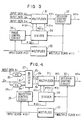
- Block diagrams of two preferred embodiments of the present invention are shown in FIG. 3 and FIG. 4.
- a multiplier 33 generates a clock ⁇ (1) having N-multiple frequency of an input clock ⁇ (o).
- N is an integer which is equal to 2 or larger than 2.
- a dividing circuit 34 generates N divided clocks ⁇ (2)1 ⁇ ⁇ (2) n by dividing the frequency of multiple clock ⁇ (1) of the multiplier 33 into 1/N.
- a multiplexing circuit 31 receives in parallel the input data D1 ⁇ D n to be converted into a series data MD1. and multiplexes input data D1 ⁇ D n in accordance with the phase of N divided clocks ⁇ (2)1 ⁇ ⁇ (2) n from the dividing circuit 34.
- the input data D1 ⁇ D n are synchronizing with each other and the input clock ⁇ (0) is also synchronizing with these input data D1 ⁇ D n .
- a decision and shaping circuit 32 discriminates "0" or "1" of the multiplex data MD1 received by circuit 32 from the multiplexing circuit 31 and shapes such data MD1 with multiple clock ⁇ (1) received from the multiplier 33.
- a phase control circuit 35 compares the phase of the input clock ⁇ (0) with that of divided clock ⁇ (2) of the dividing circuit 34 and controls the output phase of divided clock ⁇ (2) of the dividing circuit 34 so that the divided clock ⁇ (2)1 ⁇ ⁇ (2) n synchronizes with the input clock ⁇ (0).
- the above embodiment is based on the concept of controlling a phase of the divided clock ⁇ (2)1 ⁇ ⁇ (2)n for improving a phase margin. Namely, by controlling a phase of the divided clock ⁇ (2)1 ⁇ ⁇ (2) n , a phase relationship between the parallel input data D1 ⁇ D n and the divided clock ⁇ (2)1 ⁇ ⁇ (2) n can be adjusted so that a phase of the divided clock is positioned at the center of a phase of the parallel input data D1 ⁇ D n .
- FIG. 4 Another preferred embodiment of the parallel-to-serial converter of the present invention is shown in FIG. 4.
- a multiplier 33 generates a multiple clock ⁇ (1) from an input clock ⁇ (0).
- a dividing circuit 34 generates N divided clocks ⁇ (2)1 ⁇ ⁇ (2) n by dividing the frequency of multiple clock ⁇ (1) from the multiplier 33 into 1/N.
- a phase shift circuit 261 ⁇ 26 n respectively shifts phases of input data D1 ⁇ Dn to be converted into d1 ⁇ d n by a predetermined value.
- a selection circuit 27 selects either input data D1 ⁇ D n or shifted input data d1 ⁇ d n .
- a multiplexing circuit 31 receives in parallel the input data D′1 ⁇ D′ n from the selection circuit 27 and multiplexes D′1 ⁇ D′ n into MD1 in accordance with the phase of N divided clock ⁇ (2)1 ⁇ ⁇ (2) n from the dividing circuit 34.
- input data D1 ⁇ D n and input clock ⁇ (0) are synchronizing with each other.
- a decision and shaping circuit 32 discriminates "0" or "1" of the multiplex data MD1 from the multiplexing circuit 31 and shapes such multiplex data MD1 with the multiple clock ⁇ (1).
- a selection control circuit 28 compares the phase of the divided clock ⁇ (2) with that of input clock ⁇ (0) and controls a changeover operation of the selection circuit 27.
- This second preferred embodiment is based on the concept of controlling a phase of the input data D1 ⁇ D n instead of the divided clock ⁇ (2)1 ⁇ ⁇ (2) n in order to improve a phase margin. Namely, by controlling a phase of the parallel input data D1 ⁇ D n , a phase relationship between the parallel input data D1 ⁇ D n and the divided clock ⁇ (2)1 ⁇ ⁇ (2) n can be adjusted so that a phase of the divided clock is positioned at the center of a phase of the parallel input data D′1 ⁇ D′ n .
- phase control circuit 35 compares the phases of input clock ⁇ (0) and divided clock ⁇ (2) and thereby controls the output phase of the dividing circuit 34 so that data is read out at the center position of the data D1 ⁇ D n to be converted by the divided clocks ⁇ (2)1 ⁇ ⁇ (2) n in the multiplexing circuit 31.
- the data read out operation is carried out at the center position of data d1 ⁇ d n to be converted by the divided clocks ⁇ (2)1 ⁇ ⁇ (2) n in the multiplexing circuit 31 and thereby the phase margin can be improved.
- FIGS. 3 and 4 Further details and explanation of the embodiments of FIGS. 3 and 4 will now be made with reference to FIGS. 6 to 11.
- FIG. 6 is a circuit diagram for the parallel-to-serial converter of FIG. 3.
- This circuit includes a multiplexing circuit 31, a decision-shaping flip-flop 32, a multiplier 33, a dividing circuit 34 and a phase comparison circuit 35.
- the dividing circuit 34 includes a flip-flop having a set pulse input terminal. When the set pulse is applied to the set pulse input terminal, the polarity of output Q (namely, the divided clock ⁇ 1) becomes "H" or "1".
- the phase comparison circuit 35 includes a NOR circuit with three inputs.
- the input clock ⁇ 0, divided clock ⁇ 1 from the dividing circuit 34 and the clock ⁇ 3′ obtained by delaying the phase of the multiple clock ⁇ 3 from the multiplier 33 with the predetermined degree are such three inputs to circuit 35.
- the set pulse ⁇ 4 is output to the set pulse input terminal of the dividing circuit 34.
- FIG. 7 is a time chart of signals thereof at respective points of the circuit of FIG. 6.
- input data D1, D2 and input clock ⁇ 0 are synchronizing with each other.
- the divided clocks ⁇ 1, ⁇ 2 are in the "L" level, corresponding NOR circuits are open and the input data D1, D2 are read out from a multiplexing circuit 31 via corresponding NOR circuits.
- the input clock ⁇ 0 has previously been adjusted in its phase so that the "H" level thereof is positioned at the center of input data D1.
- the phases of divided clocks ⁇ 1, ⁇ 2 are adjusted with reference to the phase of this clock input ⁇ 0.
- the output phase of dividing circuit 34 is adjusted so that the polarities of input clock ⁇ 0 and divided clock ⁇ 1 have inverted polarities with each other.
- This polarity inversion can be achieved by outputting the set pulse ⁇ 4 to invert the polarities of outputs Q, Q of the dividing circuit 34 when both input clock ⁇ 0 and divided clock ⁇ 1 are in the "L" level (refer to time t1 in FIG. 7). Thereafter, the input data D1, D2 are thereby read out respectively by the divided clocks ⁇ 1, ⁇ 2 at the center position of these clocks.
- the clock ⁇ 3′ to be input to the phase comparison circuit 35 is used for narrowing the comparison period so that an erroneous set pulse is no longer output due to the existence of noise at the time of comparing the input clock ⁇ 0 with the divided clock ⁇ 1.
- FIG. 8 is another alternative circuit diagram for the parallel-to-serial converter embodiment of FIG. 3.
- the phase adjustment of divided clocks ⁇ 1, ⁇ 2 is carried out by inhibiting the multiple clock ⁇ 3 to be input to the dividing circuit 34.
- the circuit of FIG. 8 includes a multiplexing circuit 31, a flip-flop 32 as a decision and shaping circuit, a multiplier 33, a dividing circuit 34, a phase comparison circuit 35-1 and an inhibit circuit 35-2.
- the functioning of phase comparison circuit 35-1 and inhibit circuit 35-2 correspond to the phase control circuit 35 of FIG. 3.
- the phase comparison circuit 35-1 has a NOR circuit 39 which receives the input clock ⁇ 0 and divided clock ⁇ 1 and a flip-flop 38 which receives an output of the NOR circuit 39 at the data input terminal D and the clock ⁇ 3′ having a predetermined phase delay of the multiple clock ⁇ 3 at the clock input terminal C of flip-flop 38.
- the output pulse ⁇ 5 of the flip-flop 38 is output to the inhibit circuit 35-2.
- the inhibit circuit 35-2 is formed by a 2-input NOR circuit and receives the input pulse ⁇ 5 and multiple clock ⁇ 3 respectively and supplies output clock ⁇ 6 to the dividing circuit 34.
- FIG. 9 is a time chart of signals at respective points of the circuit of FIG. 8.
- the polarity of divided clock ⁇ 1 is inverted from the normal polarity, it is detected (refer to the time t1 in FIG. 7) in the phase comparison circuit 35-1 from the fact that both input clock ⁇ 0 and divided clock ⁇ 1 are in the "0" or "L” level at the rising edge of the clock ⁇ 3′.
- the output pulse ⁇ 5 is sent to the inhibit circuit 35-2 and one pulse of the multiple clock ⁇ 3 inhibited by this inhibit circuit 35-2 is extracted and then supplied to the dividing circuit 34 as the clock ⁇ 6.
- FIG. 10 A circuit diagram for the converter embodiment of FIG. 4 is shown in FIG. 10.
- the phases of input data D1, D2 are shifted by ⁇ (radian) (instead of the FIG. 3 converter where the polarities of divided clocks ⁇ 1, ⁇ 2 are inverted) when the phases of divided clocks ⁇ 1, ⁇ 2 for reading out the input data D1, D2 are inverted with respect to the phase of the input clock ⁇ 0.
- FIG. 11 is a timing chart illustrating signal waveforms at respective points of the circuit of FIG. 10.
- the input clock ⁇ 0 has previously been adjusted in its phase so that the "H” or "1" level thereof is positioned at the center of input data D1. See FIGS. 11(a) and (b).
- This circuit of FIG. 10 includes phase delay circuits 261, 262 for delaying input data D1, D2 with ⁇ rad respectively. See FIGS. 11(b),(c) and (h), and (i)). That is, the polarities of input data D1, D2 are inverted.
- a selection circuit 27 selects either one of the input data D1, D2 or delayed data d1, d2 in accordance with selection signals SEL1 and SEL2 from a control circuit 28.
- a control circuit 28 compares a phase of the clock ⁇ 0 with that of the divided clock ⁇ 1 and controls changeover operation of selection circuit 27 depending on the result of the comparison.
- the input clock ⁇ 0 is adjusted so that the "H" level thereof is positioned at the center of an input data D1 (FIGS. 11(a) and (b)).
- a control circuit comprises a flip-flop for comparing the phases of the input clock ⁇ 0 and the divided clocks ⁇ 1 and ⁇ 2
- this control circuit 28 cannot compare the phases if the phase of the input clock ⁇ 0 coincides with the phase of the divided clocks ⁇ 1 and ⁇ 2, due to the nature of a flip flop.
- the phases of the divided clock ⁇ 1 and ⁇ 2 from divided circuit 34 are adjusted to add ⁇ rad delay by buffer 54 and delay circuit 51(FIGS. 11 (a), (e) or (g)), so that a flip-flop of control circuit 28 can compare the phase relationship between the input clock ⁇ 0 and a divided clock ⁇ 1, that is, between the input data D1 and a divided clock ⁇ 1.
- a selection signal SEL1 which is an output from Q terminal of control circuit 28, is at an "L” level
- a selection signal SEL2 which is an output from Q terminal of control circuit 28, is at an "H” level
- a selection circuit 27 selects input data D1 and D2 for outputs D′1 and D′2 (FIGS. 11(b),(h)). Consequently, a multiplexer converts parallel input data D′1 and D′2 into a serial multiplexed data MD1 as shown in FIG. 11(j).
- a phase of a multiple clock is adjusted by buffer 52 as shown in FIG. 11(1).
- selection signals SEL1 and SEL2 from control circuit 50 turn into "H” and "L” level, respectively.
- selection circuit 27 selects input data d1 and d2 for outputs D′l and D′2 (FIG. 11(c),(i)).
- a multiplexer then converts parallel input data D′1 and D′2 into a serial multiplexed data MD1 as shown in FIG. 11(m).
- a multiple clock ⁇ 3 is delayed by buffer 52 like FIG. 11(o).
- a buffer 53 is just a timing interface to a next circuit and includes a flip-flop.
Landscapes
- Engineering & Computer Science (AREA)
- Theoretical Computer Science (AREA)
- Synchronisation In Digital Transmission Systems (AREA)
- Time-Division Multiplex Systems (AREA)
Applications Claiming Priority (2)
| Application Number | Priority Date | Filing Date | Title |
|---|---|---|---|
| JP63148662A JPH0773219B2 (ja) | 1988-06-16 | 1988-06-16 | 並直列変換装置 |
| JP148662/88 | 1988-06-16 |
Publications (3)
| Publication Number | Publication Date |
|---|---|
| EP0346896A2 true EP0346896A2 (de) | 1989-12-20 |
| EP0346896A3 EP0346896A3 (en) | 1990-11-28 |
| EP0346896B1 EP0346896B1 (de) | 1993-12-29 |
Family
ID=15457817
Family Applications (1)
| Application Number | Title | Priority Date | Filing Date |
|---|---|---|---|
| EP89110879A Expired - Lifetime EP0346896B1 (de) | 1988-06-16 | 1989-06-15 | Parallel/Serienumsetzer |
Country Status (5)
| Country | Link |
|---|---|
| US (1) | US4965797A (de) |
| EP (1) | EP0346896B1 (de) |
| JP (1) | JPH0773219B2 (de) |
| CA (1) | CA1304845C (de) |
| DE (1) | DE68911761T2 (de) |
Cited By (12)
| Publication number | Priority date | Publication date | Assignee | Title |
|---|---|---|---|---|
| EP0466592A1 (de) * | 1990-07-11 | 1992-01-15 | Bull S.A. | Vorrichtung zu Parallelserien und zur Serienparallelwandlung von Daten und dadurch entstandenes serielles digitales Nachrichtenübertragungssystem |
| EP0477582A1 (de) * | 1990-09-26 | 1992-04-01 | International Business Machines Corporation | Digitale Frequenzmultiplikation und Datenserialisierungsschaltkreis |
| EP0479296A1 (de) * | 1990-10-02 | 1992-04-08 | Nec Corporation | Seriell-parallel Konverter-Schaltkreis |
| US5260608A (en) * | 1990-02-06 | 1993-11-09 | Bull, S.A. | Phase-locked loop and resulting frequency multiplier |
| EP0407082A3 (en) * | 1989-07-07 | 1994-05-25 | Inmos Ltd | Clock generation |
| FR2727587A1 (fr) * | 1994-11-30 | 1996-05-31 | Sgs Thomson Microelectronics | Dispositif de serialisation de donnees binaires a haut debit |
| WO1997037451A1 (en) * | 1996-03-29 | 1997-10-09 | Dsc Communications Corporation | Multi-rate transmission system |
| WO1997049186A1 (en) * | 1996-06-20 | 1997-12-24 | Telefonaktiebolaget Lm Ericsson (Publ) | Serial-parallel and parallel-serial converter |
| EP0974888A1 (de) * | 1998-07-18 | 2000-01-26 | PIRELLI CAVI E SISTEMI S.p.A. | Optische Einheit für die Verarbeitung einer vorbestimmten optischen Reihenfolge von N-Bits |
| US6150855A (en) * | 1990-02-06 | 2000-11-21 | Bull, S.A. | Phase-locked loop and resulting frequency multiplier |
| KR100309618B1 (ko) * | 1996-12-13 | 2001-11-15 | 칼 하인쯔 호르닝어 | 병렬/직렬 변환기 |
| WO2011150172A1 (en) * | 2010-05-28 | 2011-12-01 | Qualcomm Incorporated | Method and apparatus to serialize parallel data input values |
Families Citing this family (20)
| Publication number | Priority date | Publication date | Assignee | Title |
|---|---|---|---|---|
| US5111455A (en) * | 1990-08-24 | 1992-05-05 | Avantek, Inc. | Interleaved time-division multiplexor with phase-compensated frequency doublers |
| US5282210A (en) * | 1992-06-01 | 1994-01-25 | International Business Machines Corporation | Time-division-multiplexed data transmission system |
| SE515076C2 (sv) * | 1992-07-01 | 2001-06-05 | Ericsson Telefon Ab L M | Multiplexor-/demultiplexorkrets |
| JPH06152556A (ja) * | 1992-10-30 | 1994-05-31 | Ando Electric Co Ltd | データ多重回路 |
| US5406607A (en) * | 1994-02-24 | 1995-04-11 | Convex Computer Corporation | Apparatus, systems and methods for addressing electronic memories |
| JP3166494B2 (ja) * | 1994-07-27 | 2001-05-14 | 松下電器産業株式会社 | 遅延検波方法および装置 |
| US5768283A (en) * | 1994-11-08 | 1998-06-16 | Washington University | Digital phase adjustment circuit for asynchronous transfer mode and like data formats |
| US5724361A (en) * | 1996-03-12 | 1998-03-03 | Lsi Logic Corporation | High performance n:1 multiplexer with overlap control of multi-phase clocks |
| US5805089A (en) * | 1996-09-05 | 1998-09-08 | Lsi Logic Corporation | Time-division data multiplexer with feedback for clock cross-over adjustment |
| US6202108B1 (en) * | 1997-03-13 | 2001-03-13 | Bull S.A. | Process and system for initializing a serial link between two integrated circuits comprising a parallel-serial port using two clocks with different frequencies |
| DE19716314A1 (de) * | 1997-04-18 | 1998-10-22 | Alsthom Cge Alcatel | Verfahren und Vorrichtung zur Addition von als Abtastwerte vorliegenden Signalen |
| US6879650B1 (en) * | 1998-09-23 | 2005-04-12 | Paradyne Corporation | Circuit and method for detecting and correcting data clocking errors |
| JP2000278141A (ja) * | 1999-03-26 | 2000-10-06 | Mitsubishi Electric Corp | マルチプレクサ |
| US6298400B1 (en) * | 1999-10-13 | 2001-10-02 | Sony Corporation | Enhancing interface device to transport stream of parallel signals to serial signals with separate clock rate using a pin reassignment |
| US6977980B2 (en) * | 2001-08-29 | 2005-12-20 | Rambus Inc. | Timing synchronization methods and systems for transmit parallel interfaces |
| US7576734B2 (en) * | 2001-10-30 | 2009-08-18 | Semiconductor Energy Laboratory Co., Ltd. | Signal line driving circuit, light emitting device, and method for driving the same |
| JP4242741B2 (ja) * | 2003-09-19 | 2009-03-25 | パナソニック株式会社 | デバッグ用信号処理回路 |
| KR100719343B1 (ko) * | 2005-02-28 | 2007-05-17 | 삼성전자주식회사 | 독립적인 클럭 소스를 기준으로 직렬 클럭을 생성하는 직렬변환기와 데이터의 직렬 전송 방법 |
| JP2013125561A (ja) * | 2011-12-14 | 2013-06-24 | Elpida Memory Inc | 半導体装置 |
| US20150229327A1 (en) * | 2014-02-12 | 2015-08-13 | Fujitsu Limited | Multiplexer |
Family Cites Families (6)
| Publication number | Priority date | Publication date | Assignee | Title |
|---|---|---|---|---|
| US4542504A (en) * | 1983-08-22 | 1985-09-17 | At&T Bell Laboratories | Shared data receiver |
| US4575860A (en) * | 1984-03-12 | 1986-03-11 | At&T Bell Laboratories | Data clock recovery circuit |
| NL8501737A (nl) * | 1985-06-17 | 1987-01-16 | At & T & Philips Telecomm | Hogere orde digitaal transmissiesysteem voorzien van een multiplexer en een demultiplexer. |
| GB2180725B (en) * | 1985-09-19 | 1989-01-25 | Stc Plc | Digital communication circuit |
| JPS6330034A (ja) * | 1986-07-23 | 1988-02-08 | Nec Corp | 多重化回路 |
| US4791488A (en) * | 1987-08-12 | 1988-12-13 | Rca Licensing Corporation | Line-locked clock signal generation system |
-
1988
- 1988-06-16 JP JP63148662A patent/JPH0773219B2/ja not_active Expired - Lifetime
-
1989
- 1989-06-15 CA CA000602838A patent/CA1304845C/en not_active Expired - Lifetime
- 1989-06-15 DE DE68911761T patent/DE68911761T2/de not_active Expired - Fee Related
- 1989-06-15 EP EP89110879A patent/EP0346896B1/de not_active Expired - Lifetime
- 1989-06-16 US US07/367,263 patent/US4965797A/en not_active Expired - Lifetime
Cited By (21)
| Publication number | Priority date | Publication date | Assignee | Title |
|---|---|---|---|---|
| EP0407082A3 (en) * | 1989-07-07 | 1994-05-25 | Inmos Ltd | Clock generation |
| US5389830A (en) * | 1989-07-07 | 1995-02-14 | Inmos Limited | Clock generation |
| US5548235A (en) * | 1990-02-06 | 1996-08-20 | Bull, S.A. | Phase-locked loop and resulting frequency multiplier |
| US5838178A (en) * | 1990-02-06 | 1998-11-17 | Bull S.A. | Phase-locked loop and resulting frequency multiplier |
| US5260608A (en) * | 1990-02-06 | 1993-11-09 | Bull, S.A. | Phase-locked loop and resulting frequency multiplier |
| US6150855A (en) * | 1990-02-06 | 2000-11-21 | Bull, S.A. | Phase-locked loop and resulting frequency multiplier |
| FR2664765A1 (fr) * | 1990-07-11 | 1992-01-17 | Bull Sa | Dispositif de serialisation et de deserialisation de donnees et systeme de transmission numerique de donnees en serie en resultant. |
| US5414830A (en) * | 1990-07-11 | 1995-05-09 | Bull, S.A. | Apparatus for serialization and deserialization of data, and resultant system for digital transmission of serial data |
| EP0466592A1 (de) * | 1990-07-11 | 1992-01-15 | Bull S.A. | Vorrichtung zu Parallelserien und zur Serienparallelwandlung von Daten und dadurch entstandenes serielles digitales Nachrichtenübertragungssystem |
| EP0477582A1 (de) * | 1990-09-26 | 1992-04-01 | International Business Machines Corporation | Digitale Frequenzmultiplikation und Datenserialisierungsschaltkreis |
| EP0479296A1 (de) * | 1990-10-02 | 1992-04-08 | Nec Corporation | Seriell-parallel Konverter-Schaltkreis |
| FR2727587A1 (fr) * | 1994-11-30 | 1996-05-31 | Sgs Thomson Microelectronics | Dispositif de serialisation de donnees binaires a haut debit |
| EP0715415A1 (de) * | 1994-11-30 | 1996-06-05 | STMicroelectronics S.A. | Vorrichtung zur Parallelserienwandlung von binären Daten mit hoher Datenrate |
| WO1997037451A1 (en) * | 1996-03-29 | 1997-10-09 | Dsc Communications Corporation | Multi-rate transmission system |
| US5867543A (en) * | 1996-03-29 | 1999-02-02 | Dsc Communications Corporation | Multi-rate transmission system |
| WO1997049186A1 (en) * | 1996-06-20 | 1997-12-24 | Telefonaktiebolaget Lm Ericsson (Publ) | Serial-parallel and parallel-serial converter |
| US6169500B1 (en) | 1996-06-20 | 2001-01-02 | Telefonaktiebolaget Lm Ericsson (Publ) | Serial-parallel and parallel-serial converter |
| KR100309618B1 (ko) * | 1996-12-13 | 2001-11-15 | 칼 하인쯔 호르닝어 | 병렬/직렬 변환기 |
| EP0974888A1 (de) * | 1998-07-18 | 2000-01-26 | PIRELLI CAVI E SISTEMI S.p.A. | Optische Einheit für die Verarbeitung einer vorbestimmten optischen Reihenfolge von N-Bits |
| WO2011150172A1 (en) * | 2010-05-28 | 2011-12-01 | Qualcomm Incorporated | Method and apparatus to serialize parallel data input values |
| US8405426B2 (en) | 2010-05-28 | 2013-03-26 | Qualcomm Incorporated | Method and apparatus to serialize parallel data input values |
Also Published As
| Publication number | Publication date |
|---|---|
| DE68911761T2 (de) | 1994-06-09 |
| EP0346896B1 (de) | 1993-12-29 |
| JPH01317026A (ja) | 1989-12-21 |
| US4965797A (en) | 1990-10-23 |
| JPH0773219B2 (ja) | 1995-08-02 |
| DE68911761D1 (de) | 1994-02-10 |
| CA1304845C (en) | 1992-07-07 |
| EP0346896A3 (en) | 1990-11-28 |
Similar Documents
| Publication | Publication Date | Title |
|---|---|---|
| EP0346896B1 (de) | Parallel/Serienumsetzer | |
| US3995119A (en) | Digital time-division multiplexing system | |
| US5022057A (en) | Bit synchronization circuit | |
| EP0921654B1 (de) | Digitale PLL Schaltung und Verfahren zur Signalrückgewinnung | |
| EP0351779B1 (de) | Anordnung zur Phasenregelung eines Taktgebers | |
| IL36446A (en) | Time divison multiplex data transmission system | |
| US5909473A (en) | Bit synchronizing circuit | |
| US7095816B2 (en) | Clock/data recovery circuit | |
| EP0379384B1 (de) | Schaltung zur Einstellung der Phase | |
| EP0878911B1 (de) | Taktgewinnungsschaltung | |
| US4977558A (en) | Demultiplexing device of synchronous multiplexing system | |
| JPH0936849A (ja) | ビット同期回路及びビット同期方式 | |
| US5726651A (en) | Device for serializing high flow of binary data | |
| US5757807A (en) | Method of and apparatus for extracting or inserting a signal in a time division multiplex communication system | |
| EP0481267B1 (de) | Rahmensynchronisierungsanordnung | |
| EP0942552A2 (de) | Überabtastende Schaltung zur Taktrückgewinnung mit beschränktem Energieverbrauch | |
| RU2271069C2 (ru) | Способ и схема синхронного приема при высокоскоростной передаче данных от абонента на центральный узел в системе оптической передачи данных | |
| US5708685A (en) | Frame synchronous signal detector | |
| EP0260603A2 (de) | Kanalumschaltungseinrichtung | |
| US5990811A (en) | Transfer clock converter for digital data | |
| KR19980033965A (ko) | 광통신 수신기용 클럭 및 데이타(Data) 복구회로 | |
| JPS6320931A (ja) | デ−タ伝送装置 | |
| JP2692476B2 (ja) | フレーム同期システム | |
| KR100204062B1 (ko) | 저속 데이타 프레임 위상 정렬기 | |
| KR100259767B1 (ko) | 위상 정렬 장치 및 방법 |
Legal Events
| Date | Code | Title | Description |
|---|---|---|---|
| PUAI | Public reference made under article 153(3) epc to a published international application that has entered the european phase |
Free format text: ORIGINAL CODE: 0009012 |
|
| AK | Designated contracting states |
Kind code of ref document: A2 Designated state(s): DE FR GB |
|
| PUAL | Search report despatched |
Free format text: ORIGINAL CODE: 0009013 |
|
| AK | Designated contracting states |
Kind code of ref document: A3 Designated state(s): DE FR GB |
|
| 17P | Request for examination filed |
Effective date: 19901127 |
|
| 17Q | First examination report despatched |
Effective date: 19921007 |
|
| GRAA | (expected) grant |
Free format text: ORIGINAL CODE: 0009210 |
|
| AK | Designated contracting states |
Kind code of ref document: B1 Designated state(s): DE FR GB |
|
| REF | Corresponds to: |
Ref document number: 68911761 Country of ref document: DE Date of ref document: 19940210 |
|
| ET | Fr: translation filed | ||
| PLBE | No opposition filed within time limit |
Free format text: ORIGINAL CODE: 0009261 |
|
| STAA | Information on the status of an ep patent application or granted ep patent |
Free format text: STATUS: NO OPPOSITION FILED WITHIN TIME LIMIT |
|
| 26N | No opposition filed | ||
| REG | Reference to a national code |
Ref country code: GB Ref legal event code: IF02 |
|
| PGFP | Annual fee paid to national office [announced via postgrant information from national office to epo] |
Ref country code: DE Payment date: 20070607 Year of fee payment: 19 |
|
| PGFP | Annual fee paid to national office [announced via postgrant information from national office to epo] |
Ref country code: GB Payment date: 20070613 Year of fee payment: 19 |
|
| PGFP | Annual fee paid to national office [announced via postgrant information from national office to epo] |
Ref country code: FR Payment date: 20070608 Year of fee payment: 19 |
|
| GBPC | Gb: european patent ceased through non-payment of renewal fee |
Effective date: 20080615 |
|
| REG | Reference to a national code |
Ref country code: FR Ref legal event code: ST Effective date: 20090228 |
|
| PG25 | Lapsed in a contracting state [announced via postgrant information from national office to epo] |
Ref country code: DE Free format text: LAPSE BECAUSE OF NON-PAYMENT OF DUE FEES Effective date: 20090101 |
|
| PG25 | Lapsed in a contracting state [announced via postgrant information from national office to epo] |
Ref country code: GB Free format text: LAPSE BECAUSE OF NON-PAYMENT OF DUE FEES Effective date: 20080615 |
|
| PG25 | Lapsed in a contracting state [announced via postgrant information from national office to epo] |
Ref country code: FR Free format text: LAPSE BECAUSE OF NON-PAYMENT OF DUE FEES Effective date: 20080630 |