EP0343317B1 - Filterkreis - Google Patents
Filterkreis Download PDFInfo
- Publication number
- EP0343317B1 EP0343317B1 EP89101802A EP89101802A EP0343317B1 EP 0343317 B1 EP0343317 B1 EP 0343317B1 EP 89101802 A EP89101802 A EP 89101802A EP 89101802 A EP89101802 A EP 89101802A EP 0343317 B1 EP0343317 B1 EP 0343317B1
- Authority
- EP
- European Patent Office
- Prior art keywords
- threshold value
- filter circuit
- count
- circuit according
- value
- Prior art date
- Legal status (The legal status is an assumption and is not a legal conclusion. Google has not performed a legal analysis and makes no representation as to the accuracy of the status listed.)
- Expired - Lifetime
Links
- 238000005070 sampling Methods 0.000 claims description 46
- 230000002441 reversible effect Effects 0.000 claims description 37
- 230000007704 transition Effects 0.000 claims description 24
- 239000013078 crystal Substances 0.000 claims description 3
- 230000001360 synchronised effect Effects 0.000 claims description 2
- 238000010586 diagram Methods 0.000 description 26
- 244000145845 chattering Species 0.000 description 9
- 238000000034 method Methods 0.000 description 5
- 238000001914 filtration Methods 0.000 description 4
- 230000010354 integration Effects 0.000 description 4
- 239000003990 capacitor Substances 0.000 description 3
- 230000000694 effects Effects 0.000 description 2
- 238000006243 chemical reaction Methods 0.000 description 1
- 230000001934 delay Effects 0.000 description 1
- 230000001419 dependent effect Effects 0.000 description 1
- 238000007599 discharging Methods 0.000 description 1
- 238000002955 isolation Methods 0.000 description 1
- 238000002789 length control Methods 0.000 description 1
- 230000000630 rising effect Effects 0.000 description 1
Images


Classifications
-
- H—ELECTRICITY
- H03—ELECTRONIC CIRCUITRY
- H03H—IMPEDANCE NETWORKS, e.g. RESONANT CIRCUITS; RESONATORS
- H03H9/00—Networks comprising electromechanical or electro-acoustic elements; Electromechanical resonators
- H03H9/46—Filters
- H03H9/48—Coupling means therefor
- H03H9/52—Electric coupling means
-
- H—ELECTRICITY
- H03—ELECTRONIC CIRCUITRY
- H03K—PULSE TECHNIQUE
- H03K5/00—Manipulating of pulses not covered by one of the other main groups of this subclass
- H03K5/125—Discriminating pulses
- H03K5/1252—Suppression or limitation of noise or interference
Definitions
- the present invention relates to a filter circuit, and more particularly to a filter circuit of the kind referred to in the preamble portion of patent claim 1.
- a filter circuit is known from US-A-4 667 338.
- a control system for a programmable controller and the like receives a state signal indicative of the state or condition of a controlled device or system and then processes such signal to generate and output a required control signal.
- the state signal i.e. an input signal of the control system
- the present invention relates to a filter circuit for performing the above-mentioned operations.
- a filter circuit for performing the above-mentioned operations.
- One of the examples of a conventional filter circuit is shown in Fig. 1, and the operating waveforms thereof are shown in Fig. 2.
- a programmable controller 10 receives a state signal S from an external device 9, which may be the controlled device or system.
- This state signal is subjected to level conversion in a circuit 11, which also provides isolation, so that the state signal S is converted into a signal 5, as shown in Fig. 2, and this signal 5 is then supplied to a capacitance-resistance (CR) filter 12.
- the signal 5 is integrated by a capacitor-resister circuit so that the noise will be removed therefrom.
- the CR filter 12 outputs the integrated signal as a filter output signal 15, the waveform of which is shaped by a receiver 13 having a hysteresis characteristic.
- the shaped signal has delays 17 and 18, respectively, at the rising and falling portions thereof.
- the "L" potential level at the input of the receiver 13 tends to be increased because of the voltage drop across the resister in the filter circuit 12, with the undesirable possibility that the "1" signal will be misjudged as a "H” signal in the receiver 13.
- the charging and discharging waveforms of the capacitor are not uniform, and due to variation of the threshold value of the receiver 13, which depends on the temperature, variation of the delay times 17 and 18 are necessarily large.
- the hysteresis characteristic depends on the threshold voltage of the receiver input, so that it is impossible to enlarge the hysteresis width of the receiver 13.
- the capacitor in the filter circuit 12 is not suitable for circuit integration.
- FIG. 3 shows an example of a conventional digital filter circuit, which is disclosed in Japanese Patent Laid-Open Publication No. 61-109317; and, Fig. 4 is a time chart showing the operation of this conventional circuit.
- a digital filter 1 receives a filter input signal 5, which is sampled at the D input of a shift register 30 driven by a sampling clock 7. If four successive signal samples of the filter input signal 5 are at the "H" level, so that all outputs Q1 to Q4 of the shift register 30 are at the "H” level, an output set signal 28 of level "L” is produced by a NAND gate 311, so that a flip-flop 301 is set.
- Japanese Patent Laid-Open Publication No. 56-114002 discloses a filter circuit which is capable of setting a variable delay time.
- the noise removal characteristic and delay time can be varied in this conventional circuit by varying the capacitor storage time of a capacitor-resistor filter, and so, the foregoing disadvantages relating to the filter circuit of Fig. 1 are also present in this conventional circuit.
- US-A-4 667 338 discloses a filter circuit comprising clock signal generating means for generating a sampling clock signal, means for two-level sampling of an input signal, a reversible counter for performing a count-up operation when a sampled value of said input signal is at the high level and a count-down operation when a sampled value of said input signal is at the low level, first control means coupled to said reversible counter for detecting a first threshold value of a count by said reversible counter, second control means coupled to said reversible counter for detecting a second threshold value of a count by said reversible counter, means for providing a filter circuit output.
- the above-mentioned objects can be achieved by providing a reversible counter which counts up or down in response to the "H" or "L" level of the input signal and which skips to an advanced count value when the count value becomes larger than a threshold value to provide an inherent hysteresis characteristic.
- the above objects can be achieved by operating a sampling clock generating circuit to generate plural clock signals each having a different frequency, and by selecting one of the plural clock signals having a frequency according to a value set by a time constant setting circuit so that the selected clock signal is set as the clock signal of the above-mentioned reversible counter.
- this reversible counter skips to an advanced count value at the time when the count value becomes larger than the threshold value, so that the count value does not revert to the count value representing the threshold value immediately, even when a noise signal of opposite polarity is inputted thereto.
- the sampling clock generating circuit generates plural clock signals, one of which is selected and then supplied to the reversible counter. Therefore, it is possible to control the counting operation of the reversible counter and also control the time constant of the filter operation. Moreover, it is easy to stabilize this clock signal, so that any variation of the time constant can be minimized.
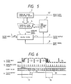
- Fig. 5 is a block diagram showing a basic configuration of the filter circuit according to the present invention.
- a digital filter 1 constituted by an up/down counter, receives a filter input signal 5, which typically includes noise and chattering components therein.
- the digital filter 1 performs count-up or countdown operations in response to the "H” or "L” level of the filter input signal 5 every time the sampling clock signal 7 is inputted thereto. As a result, the digital filter 1 outputs a filter output signal 6 from which the noise is removed.
- One clock signal identified by the time constant (or delay time) setting circuit 3 is selected from plural clock signals of different frequency, which are obtained by dividing a basic clock input signal 42 in a clock signal generating circuit 2 by a sampling clock selecting circuit 4, so that such selected clock signal is set as the sampling clock signal 7 supplied to the digital filter 1.
- the filter input waveform 5 including the highest degree of noise and chattering etc., is sampled by the sampling clock signal 7, and a count value is incremented when the sampled filter input waveform has the "H" level (as shown by hollow circles), while the count value is decremented when the sampled filter input waveform is at the "L" level (as shown by black circles).
- the counting operation is controlled according to the following rules. When the count value is incremented over three, the filter output signal 6 is set to have the "H" level and the count is advanced to seven.
- the filter output signal 6 When the count value is decremented below four, the filter output signal 6 is set to have the "L" level and the count is jumped to zero. By using an up/down counter in this way, the counter value is changed from zero to one, but is not incremented over three unless the proper succession of positive pulses is detected. Even if a positive pulse (or noise) 24 shown in Fig. 6 is inputted to the digital filter 1 during a sequence of negative pulses, the filter output signal 6 is not effected by this positive pulse 24, so that the noise can be removed from the filter input signal 5. Similarly, in the case where negative pulses 22, 23 and 24 etc.
- the pulse removal ability of the filter in accordance with the invention can be expressed by the following equation. For this reason, it is possible to obtain the ideal low-pass filtering characteristic which can remove all pulses having a pulse width satisfying this equation.
- (Removable Maximum Pulse Width) (Sampling Clock Period: Ts) x (Count Distance to Threshold Value)
- the filtering characteristic obtained by the present embodiment will be identified as a function whose value depends on the sampling clock period Ts only. Therefore, in the case where the basic clock signal is generated by use of a crystal oscillator etc., there is an advantage in that it is possible to obtain a stable filtering characteristic having a high accuracy.
- the count value is incremented over three, the next count value is not set to four, but is set to seven as shown by time slot 19, Thus, even if the negative pulse 43 is inputted to the digital filter 1 just after the level of the filter output waveform 6 changes to the "H" level, the count value is decremented to six, for example. In this case, there is a gap between the count value of six and the threshold value of four, so that it is possible to prevent the level of the filter output signal from being inverted to the "L" level again by a single pulse of opposite polarity.
- the next count value is not decremented to three, but is set to Zero, as shown by time slot 20, so that it is possible to prevent the filter output waveform from being inverted to the positive or "H" level again by a single positive pulse 24. Therefore, no chattering is produced in the filter output waveform 6 as a result of this built-in hysteresis.
- the hysteresis width is set to 4Ts (Ts: sampling clock period).
- this hysteresis width can be freely varied from 2Ts to 4Ts by varying the count distance to be jumped when the count value is incremented over the threshold value. This is shown in Figs. 7(a) through 7(c).
- Figs. 7(a) through 7(c) show state transition diagrams indicating the relation between the counting operation of a reversible counter of three bits and the hysteresis width.
- the suffix number "S" directly corresponds to the count value of the up/down counter in each state.
- the value of the filter output signal Y equals "1" when the count value is over "4", while such value of the filter output signal Y equals "0" when the count value is below “3".
- the value of the filter output signal Y equals the value of most significant bit (MSB) of the counter.
- MSB most significant bit
- X refers to "H” samples
- X refers to "L” samples.
- the jump count distance 4, as described in Fig. 6, corresponds to the diagram shown in Fig. 7(a), which is an example for setting the hysteresis width to the maximum.
- Fig. 7(b) illustrates a jump count distance of 3
- Fig. 7(c) shows a jump count distance of 2.
- the hysteresis width set as described above depends on N times the sampling clock period, where N is an integer.
- Fig. 8 is a state transition diagram which is obtained by adding a reset operation to the state transition diagram shown in Fig. 7(a) reset operation responsive to an applied reset signal 8, as shown in Fig. 5
- the value in parenthesis in each state indicates the count value of the up/down counter.
- Fig. 9 is a circuit diagram showing an example of a digital filter which is constituted by a master-slave JK flip-flop and which operates according to the state transition diagram of Fig. 8.
- a JK flip-flop 25 designates the least significant bit of an up/down counter
- a JK flip-flop 26 designates a middle bit
- a JK flip-flop 27 designates the most significant bit (MSB) thereof.
- the reset operation is executed by setting the J input of each flip-flop to the "L" level, and also by setting the K input of each flip-flop to the "H” level.
- the counting operation is executed by respectively controlling the J and K inputs of each flip-flop at every sampling clock timing based on the output state of each flip-flop and the state of the input signal 5.
- the number of gates is small; hence, this embodiment is not only effective in removing the chattering and noise from applied input signals, but is easy to fabricate.
- Fig. 10 shows another embodiment of the digital filter which is constituted so as to directly control the variation of each bit based on a state transition diagram.
- the digital filter 1 shown in Fig. 5 also can be constituted as shown in the block diagram of Fig. 10.
- the filter input signal 5 is inputted to the presetable reversible up/down counter 31 to thereby initiate by its logic level a count-up operation mode or a countdown operation mode.
- the sampling clock signal 7 starts the counting operation, and the output signal of the reversible counter 31 is monitored by threshold value detecting circuits 44 and 45. When the value of this output signal reaches the preset threshold value, the threshold value detecting circuits 44 and 45 output threshold detecting signals 62 and 63 .
- a preset command generating circuit 46 Based on these threshold detecting signals 62 and 63 , a preset command generating circuit 46 generates a preset command 34 and a preset data generating circuit 47 generates preset data 35.
- the preset command 34 and the preset data 35 are supplied to the reversible up/down counter 31.
- the count value is forcibly preset to the proper value depending on the current output of the reversible counter 31, so that the counting operation is executed discontinuously. Hence, it is possible to obtain a satisfactory hysteresis characteristic.
- Fig. 11 shows a more specific example of the embodiment shown in Fig. 10.
- a synchronous binary reversible up/down counter 31 of four bits is used as the up/down counter so as to provide an operation involving sixteen states, in which the threshold is eight rather than four.
- this circuit shown in Fig. 11 uses an ordinary up/down counter. Therefore, in the case where a general-purpose logical IC is used for realizing this embodiment, it can be said that this embodiment provides an advantage because of the small number of elements required.
- Fig. 12 shows a time chart of the operation of the embodiment of Fig. 11.
- the turn-on threshold value detecting signal 62 takes the "L” level, so that the level of the filter output signal 6 becomes “H” at the input timing of the sampling clock, i.e. as the reversible counter 31 increments.
- the turn-off threshold value detecting signal 63 takes the logic "L” level so that the level of the filter output signal 6 becomes “L” at the input timing of the sampling clock, i.e. as the reversible counter 31 decrements.
- the reset operation by forcibly presetting the counter to zero by means of the reset signal 8.
- the output data signal 35 of the preset data generating circuit 47 is set to indicate zero or fifteen depending on the current state of the reversible counter 31.
- the hysteresis width can be reduced from 8Ts to 7Ts by presetting the circuit 47 to produce one and fourteen.
- the digital filter is constituted by use of a binary up/down counter.
- the counter to be used in accordance with the present invention is not necessarily limited to a binary up/down counter.
- the present invention basically uses a reversible counter and provides hysteresis to the state transition at the time the count value is incremented or decremented past a threshold value.
- a counter in this way, it is possible to provide a digital filter having a satisfactory hysteresis.
- Figs. 7(a) through 7(c) described previously are state transition diagrams for a digital filter using a binary up/down counter in the case of eight states, in accordance with the present invention, and Fig. 7(a) shows the largest pulse removal ability and hysteresis width.
- Fig. 7(a) shows the largest pulse removal ability and hysteresis width.
- N flip-flops N flip-flops in general.
- the output is subjected to the states shown in the state transition diagram having the hysteresis as shown in Fig. 7(a), but without the use of a binary counter.
- Fig. 13 shows an embodiment based on this concept.
- the value in parentheses in each state indicates one example of an assigned count value corresponding to each state, and an important feature of this invention is that this assignment can be arbitrarily performed.
- This embodiment shows an example of an assignment according to the characters of m bits in the case where only one bit number must be varied in the transition between the adjacent states.
- a comparison of Figs. 8 and 13 will show that the count values for the states S2, S3, S6 and S7 are different in the respective diagrams.
- Fig. 14 shows one of a filter circuit in accordance with the state transition diagram of Fig. 13.
- a D flip-flop 48 designates the least significant bit (LSB)
- a D flip-flop 49 designates a middle bit
- a D flip-flop 50 designates the most significant bit (MSB).
- the reset operation is executed by supplying a clear input to the D flip-flop of each bit.
- the reversible counting operation is executed by controlling the D inputs of the D flip-flops 48 to 50 based on the filter input signal 5 and the output state of each flip-flop. As described above, the reversible counter counts its count value by m bits.
- control logic of the input of each bit in the flip-flop can be simplified, and a small number of gates is needed.
- the present embodiment is advantageous for large scale circuit integration (LSI) of a gate array and the like in the case where a significant number of input signals are processed by the filter.
- LSI large scale circuit integration
- the sampling clock generating circuit 2 generates plural sampling clocks each having a different frequency, as mentioned above, and one of these sampling clock signals is selected by the sampling clock selecting circuit 4 in accordance with the value set by the time constant setting circuit 3.
- the sampling clock selecting circuit 4 it is possible to vary the period of the sampling clock signal supplied to the digital filter 1, and it is also possible to vary the time constants corresponding to the maximum removal pulse width and input/output delay time. For example, in the time chart shown in Fig.
- the turn-on delay time 17 is determined by when the output level changes to the "H” level by counting how many times the sampled input level is at the "H” level. Therefore, when the "H" levels are continuously sampled, the delay time becomes equal to 3Ts to 4Ts.
- the delay time becomes equal to 5Ts to 6Ts.
- one-time sampling of the "L" level greatly enlarges the delay time from 3Ts to 7Ts and 8Ts in the conventional filter circuit shown in Fig. 3. Compared to the conventional filter circuit, it is possible to obtain a stable operation in an advantageous way in accordance with the present invention.
- both the maximum delay time and the maximum removable pulse width can be expressed by a function whose value depends on the sampling period Ts.
- these values can be varied by varying the sampling period Ts as described in the embodiment shown in Fig. 5. Therefore, in the case where the filter circuit according to the present invention is adopted for an input portion 38 of a programmable controller 10, as shown in Fig. 15, it is possible to reduce the delay time by supplying a sampling clock having a short period to the digital filter when the external device demands a fast response. In addition, in the case where the external device 9 does not demand such a fast response, it is possible to sufficiently remove the noise and chattering by supplying a sampling clock signal having a long period to the digital filter.
- Ts Program Scan Time
- the program scan time equals one process time (or one execution time) when the operation portion 14 repeatedly executes a control program stored in a storing portion 40 in the programmable controller 10. Therefore, in the case where the above condition is satisfied, it is possible to perform the operation based on the new input signal data at every process, so that it is possible to practically use the process speed of the operation portion.
- the sampling period Ts must be determined to satisfy the following relation: (State Transition Distance to Threshold Value) x (Sampling Period: Ts) ⁇ 1/2 x (Maximum Frequency of Input Signal: f max ) ⁇ Ts ⁇ 1/2f max x (State Transition Distance to Threshold Value) (5) Meanwhile, in case of an external device in which a speedy response is not demanded, the sampling clock period is set in response to the characteristic of the device connected to the input portion 38 so that the inputted chatter
- the maximum removable pulse width can be set to 10 msec. This can be expressed by the following relation: (Maximum Removable Pulse Width) ⁇ ( Maximum Pulse Width of Input Noise) (6) Hence, based on the relations (2) and (6), the sampling period must be set to the contact so that the following relation will be satisfied: Ts ⁇ (Maximum Pulse Width of Input Noise)/(State Transition Distance to Threshold Value) (7) It is possible to provide a plurality of time constant setting circuits 3 and sampling clock selecting circuits 4 by which the different sampling clock signals are supplied respectively to process a plurality of input signals. Fig.
- FIG. 16 shows one embodiment in this case.
- two 2-bit registers which can set the value from the operation portion are provided as the time constant setting means 3
- a frequency dividing counter is provided as the sampling clock generating circuit 2
- two data selectors which can select one data signal from four inputted data signals are provided as the sampling clock selecting circuit 4. Therefore, different set values are written into two time constant setting registers 3 whose outputs are independently selected by two data selectors 4 to thereby obtain two sampling clock signals 7, which are supplied to plural digital filters 1.
- the time constant setting circuit 3 shown in Fig. 5 by a switch, register or other conventional device.
- a known oscillator circuit which directly generates plural clock signals.
- the sampling clock signal 7 which is supplied to the digital filter 1 can be supplied from a variable frequency oscillator.
- the present invention Since the present invention has a large hysteresis width and high pulse removal ability, resistance quantities of chattering and noise for the input waveform can be improved.
- there are no capacitances included in the circuit according to the present invention so that a characteristic stabilized against temperature can be obtained and the present invention is suitable for circuit integration.
- the time constant can be varied by varying the clock frequency, so that it is possible to reduce the delay time for the input signs which needs high speed input. Furthermore, it is possible to obtain an optimum filtering characteristic against the noise which depends on environment and power conditions, and the stability of the delay time can be remarkably improved.
Landscapes
- Physics & Mathematics (AREA)
- Nonlinear Science (AREA)
- Acoustics & Sound (AREA)
- Manipulation Of Pulses (AREA)
- Input From Keyboards Or The Like (AREA)
- Measuring Frequencies, Analyzing Spectra (AREA)
Claims (14)
- Filterkreis mit- einer Taktsignalerzeugungseinrichtung (2) zur Erzeugung eines Abtasttaktsignals,- einer Einrichtung (4) zum Abtasten von zwei Ebenen eines Eingangssignals,- einem reversierbaren Zähler (31) zum Ausfuhren einer Vorwartszähloperation, wenn sich ein abgetasteter Wert des Eingangssignals auf einem hohen Pegel, und einer Rückwärtszähloperation, wenn sich ein abgetasteter Wert des Eingangssignals auf einem niedrigen Pegel befindet,- einer mit dem reversierbaren Zähler (31) gekoppelten ersten Regeleinrichtung (44) zum Erfassen eines ersten Schwellenwerts eines Zählwerts des reversierbaren Zählers (31),- einer mit dem reversierbaren Zähler (31) gekoppelten zweiten Regeleinrichtung (45) zum Erfassen eines zweiten Schwellenwerts eines Zählwerts des reversierbaren Zählers (31)- einer Einrichtung zum Vorsehen eines Filterkreisausgangs (6),dadurch gekennzeichnet, daß- die erste Regeleinrichtung (44) zum Einstellen des Zählwerts des reversierbaren Zählers (31) auf einen Wert vorgesehen ist, der gleich dem ersten Schwellenwert plus einem vorgegebenen Wert ist, wenn der Zählwert über dem ersten Schwellenwert liegt,- die zweite Regeleinrichtung (45) zum Einstellen des Zählwerts des reversierbaren Zählers (31) auf einen Wert vorgesehen ist, der gleich dem zweiten Schwellenwert minus dem vorgegebenen Wert ist, wenn der Zählwert unter dem ersten Schwellenwert liegt, und- daß der Ausgang des signifikantesten Bits (MSB) des reversierbaren Zählers als Filterkreisausgang vorgesehen ist.
- Filterkreis gemäß Anspruch 1, in dem der reversierbare Zähler ein synchroner, binärer Vorwärts/Ruckwärtszähler (31) ist.
- Filterkreis gemäß Anspruch 1, in dem die erste Regeleinrichtung und die zweite Regeleinrichtung entsprechende logische Gatter umfassen, die die Ausgänge des Vorwärts/Rückwärtszählers mit dessen Eingängen verbinden.
- Filterkreis gemäß Anspruch 1, in dem der reversierbare Zähler mehrere Flipflops (25, 26, 27) umfaßt, die durch eine Logikgatteranordnung miteinander verbunden sind.
- Filterkreis gemäß Anspruch 1, in dem der erste Schwellenwert drei, der zweite Schwellenwert vier und der vorgegebene Wert vier ist.
- Filterkreis gemäß Anspruch 1 in dem der erste Schwellenwert sieben, der zweite Schwellenwert acht und der vorgegebene Wert acht ist.
- Filterkreis gemäß Anspruch 1, in dem der erste Schwellenwert anders als der zweite Schwellenwert ist und der vorgegebene Wert gleich dem ersten Schwellenwert ist.
- Filterkreis gemäß Anspruch 1, in dem der erste Schwellenwert anders als der zweite Schwellenwert ist und der vorgegebene Wert gleich dem zweiten Schwellenwert ist.
- Filterkreis gemäß Anspruch 1, in dem der erste Schwellenwert, der zweite Schwellenwert und der vorgegebene Wert voneinander verschieden sind.
- Filterkreis gemäß Anspruch 1, in dem die Taktsignalerzeugungseinrichtung (2) einen Kristalloszillator umfaßt.
- Filterkreis gemäß Anspruch 1 in dem die Taktsignalerzeugungseinrichtung (2) umfaßt:- eine Erzeugungseinrichtung (36) zum Erzeugen mehrerer Taktsignale, von denen jedes eine unterschiedliche Frequenz aufweist, und- eine Auswahleinrichtung zum Auswählen eines durch die Erzeugungseinrichtung erzeugten Taktsignals und zum Ausgeben des ausgewählten Tatksignals als Abtasttaktsignal.
- Filterkreis gemäß Anspruch 11, in dem die Erzeugungseinrichtung einen Kristalloszillator umfaßt, der mit einem Frequenzteiler verbunden ist.
- Filterkreis gemäß Anspruch 1, in dem der reversierbare Zähler mehrere Flipflops (48, 49, 50) umfaßt, die durch eine Logikschaltkreisanordnung miteinander verbunden sind, um eine Sequenz von Zählwertzuständen zu erzeugen, von denen jeder einen beliebig zugeordneten Zählwert aufweist.
- Filterkreis gemäß Anspruch 13, in dem die Zählwerte der angegebenen Sequenz von Zählwertzuständen derart zugeordnet sind, daß nur eine Bitzahl im Übergang zwischen den benachbarten Zählwertzuständen in der genannten Sequenz geändert wird.
Applications Claiming Priority (2)
| Application Number | Priority Date | Filing Date | Title |
|---|---|---|---|
| JP63127183A JP2585372B2 (ja) | 1988-05-26 | 1988-05-26 | フイルタ回路 |
| JP127183/88 | 1988-05-26 |
Publications (3)
| Publication Number | Publication Date |
|---|---|
| EP0343317A2 EP0343317A2 (de) | 1989-11-29 |
| EP0343317A3 EP0343317A3 (en) | 1990-01-24 |
| EP0343317B1 true EP0343317B1 (de) | 1993-11-03 |
Family
ID=14953730
Family Applications (1)
| Application Number | Title | Priority Date | Filing Date |
|---|---|---|---|
| EP89101802A Expired - Lifetime EP0343317B1 (de) | 1988-05-26 | 1989-02-02 | Filterkreis |
Country Status (6)
| Country | Link |
|---|---|
| US (1) | US4961014A (de) |
| EP (1) | EP0343317B1 (de) |
| JP (1) | JP2585372B2 (de) |
| KR (1) | KR890017866A (de) |
| DE (1) | DE68910379T2 (de) |
| ES (1) | ES2045209T3 (de) |
Families Citing this family (22)
| Publication number | Priority date | Publication date | Assignee | Title |
|---|---|---|---|---|
| JP2585372B2 (ja) | 1988-05-26 | 1997-02-26 | 株式会社日立製作所 | フイルタ回路 |
| DE4236626C2 (de) * | 1992-10-29 | 2002-02-28 | Siemens Ag | Filterverfahren |
| US5451852A (en) * | 1993-08-02 | 1995-09-19 | Gusakov; Ignaty | Control system having signal tracking window filters |
| JPH09214289A (ja) * | 1996-01-30 | 1997-08-15 | Uniden Corp | フィルタ回路 |
| JP3849892B2 (ja) * | 1996-09-09 | 2006-11-22 | ソニー株式会社 | フイルタ装置及び無線通信端末装置 |
| JP3220029B2 (ja) * | 1996-11-11 | 2001-10-22 | 日本電気株式会社 | 入力信号読み取り回路 |
| KR100232017B1 (ko) * | 1997-06-03 | 1999-12-01 | 김영환 | 업/다운 전환 카운터 |
| DE59913064D1 (de) | 1998-10-14 | 2006-04-06 | Continental Teves Ag & Co Ohg | Verfahren und schaltungsanordnung zur signalverarbeitung für einen bewegungssensor |
| US6536029B1 (en) * | 1999-03-15 | 2003-03-18 | Siemens Energy & Automation | Programmable logic controller method, system and apparatus |
| DE19948892C2 (de) * | 1999-10-11 | 2002-07-18 | Asm Automation Sensorik Messte | Impulsdetektor und Verfahren zur Detektion von sinusförmigen Impulsen |
| EP1137180A1 (de) * | 2000-03-22 | 2001-09-26 | Infineon Technologies AG | Digitales Tiefpassfilter für digitale Signale und Verfahren zur Verarbeitung eines digitalen Signales |
| JP2002310728A (ja) * | 2001-04-13 | 2002-10-23 | Matsushita Electric Ind Co Ltd | パルス信号フィルタリング回路 |
| US6707874B2 (en) | 2002-04-15 | 2004-03-16 | Charles Douglas Murphy | Multiple-output counters for analog-to-digital and digital-to-analog conversion |
| JP2003338132A (ja) * | 2002-05-20 | 2003-11-28 | Teac Corp | 信号処理回路 |
| EP2052335A4 (de) | 2006-08-18 | 2010-11-17 | Sony Corp | System und verfahren für selektiven zugriff auf medieninhalte über einen empfehlungsmotor |
| JP2009217539A (ja) * | 2008-03-11 | 2009-09-24 | Koyo Electronics Ind Co Ltd | 入力データフィルタ方法およびその方法の実施に用いる入力データフィルタ装置 |
| US8581595B2 (en) * | 2008-08-15 | 2013-11-12 | Spansion Llc | Method of measuring flash memory cell current |
| JP5086306B2 (ja) * | 2009-05-26 | 2012-11-28 | 株式会社日立産機システム | プログラマブルコントローラ |
| WO2015186175A1 (ja) * | 2014-06-02 | 2015-12-10 | 三菱電機株式会社 | ノイズ解析装置、電子装置、及びノイズ源特定システム |
| CN107947786A (zh) * | 2017-11-16 | 2018-04-20 | 湖南工业大学 | 翻斗式雨量计计数脉冲产生方法 |
| CN107979358A (zh) * | 2017-11-16 | 2018-05-01 | 湖南工业大学 | 按键脉冲去抖动方法 |
| WO2025004876A1 (ja) * | 2023-06-28 | 2025-01-02 | 三菱電機株式会社 | 信号処理回路 |
Family Cites Families (9)
| Publication number | Priority date | Publication date | Assignee | Title |
|---|---|---|---|---|
| JPS56138330A (en) * | 1980-03-31 | 1981-10-28 | Matsushita Electric Works Ltd | Noise rejector for constant input judgement |
| JPS5787232A (en) * | 1980-11-18 | 1982-05-31 | Mitsubishi Electric Corp | Input signal reading circuit |
| US4423383A (en) * | 1982-03-05 | 1983-12-27 | Ampex Corporation | Programmable multiple frequency ratio synchronous clock signal generator circuit and method |
| JPS5977717A (ja) * | 1982-10-27 | 1984-05-04 | Matsushita Electric Ind Co Ltd | デイジタルフイルタ |
| US4556842A (en) * | 1983-07-26 | 1985-12-03 | Westinghouse Electric Corp. | Tracking filter for sensing DC content in an AC waveform |
| US4667338A (en) * | 1984-06-01 | 1987-05-19 | Sanyo Electric Co., Ltd. | Noise elimination circuit for eliminating noise signals from binary data |
| JPS61109317A (ja) * | 1984-11-02 | 1986-05-27 | Hitachi Ltd | インタフエ−ス回路 |
| JPS62245814A (ja) * | 1986-04-18 | 1987-10-27 | Fujitsu Ltd | パルス回路 |
| JP2585372B2 (ja) | 1988-05-26 | 1997-02-26 | 株式会社日立製作所 | フイルタ回路 |
-
1988
- 1988-05-26 JP JP63127183A patent/JP2585372B2/ja not_active Expired - Lifetime
-
1989
- 1989-01-30 KR KR1019890000994A patent/KR890017866A/ko not_active Abandoned
- 1989-02-02 ES ES89101802T patent/ES2045209T3/es not_active Expired - Lifetime
- 1989-02-02 DE DE89101802T patent/DE68910379T2/de not_active Expired - Fee Related
- 1989-02-02 EP EP89101802A patent/EP0343317B1/de not_active Expired - Lifetime
- 1989-02-13 US US07/309,423 patent/US4961014A/en not_active Expired - Lifetime
Also Published As
| Publication number | Publication date |
|---|---|
| KR890017866A (ko) | 1989-12-18 |
| ES2045209T3 (es) | 1994-01-16 |
| JPH01297913A (ja) | 1989-12-01 |
| EP0343317A2 (de) | 1989-11-29 |
| DE68910379D1 (de) | 1993-12-09 |
| JP2585372B2 (ja) | 1997-02-26 |
| US4961014A (en) | 1990-10-02 |
| DE68910379T2 (de) | 1994-04-14 |
| EP0343317A3 (en) | 1990-01-24 |
Similar Documents
| Publication | Publication Date | Title |
|---|---|---|
| EP0343317B1 (de) | Filterkreis | |
| US4657406A (en) | Timing generating device | |
| EP0177557B1 (de) | Zählvorrichtung und verfahren zur musternahme von frequenzen | |
| EP0025651A2 (de) | Signal-Umwandlerschaltung und numerisches Steuergerät mit einer solchen Schaltung | |
| US3961271A (en) | Pulse width and amplitude screening circuit | |
| US5065047A (en) | Digital circuit including fail-safe circuit | |
| GB2144935A (en) | Device for measuring the time between two events | |
| EP0066265B1 (de) | Digital-Analog-Umsetzer | |
| EP0662755A1 (de) | Sägezahngeneratorschaltung | |
| US4164712A (en) | Continuous counting system | |
| SU888335A1 (ru) | Цифровой фильтр | |
| KR100205922B1 (ko) | 단안정 멀티바이브레이터 | |
| KR100275684B1 (ko) | 디지탈필터 | |
| SU1157674A1 (ru) | Цифровой селектор импульсов по длительности | |
| SU1270879A1 (ru) | Многоканальный программируемый генератор импульсов | |
| SU824146A2 (ru) | Устройство дл программного управлени | |
| SU1683037A1 (ru) | Устройство дл решени задач на графах | |
| SU1049899A1 (ru) | Устройство ранжировани экстремальных значений | |
| KR0130882Y1 (ko) | 디지탈 노이즈 필터 | |
| SU1707762A1 (ru) | Быстродействующий управл емый делитель частоты | |
| SU1653153A1 (ru) | Делитель частоты с переменным коэффициентом делени | |
| SU1383473A1 (ru) | Преобразователь серии импульсов в пр моугольный импульс | |
| SU1241468A2 (ru) | Делитель частоты следовани импульсов с регулируемой длительностью импульсов | |
| SU1422363A1 (ru) | Цифрова регулируема лини задержки | |
| SU732910A1 (ru) | Устройство дл логарифмировани частотных сигналов |
Legal Events
| Date | Code | Title | Description |
|---|---|---|---|
| PUAI | Public reference made under article 153(3) epc to a published international application that has entered the european phase |
Free format text: ORIGINAL CODE: 0009012 |
|
| AK | Designated contracting states |
Kind code of ref document: A2 Designated state(s): DE ES FR IT NL |
|
| PUAL | Search report despatched |
Free format text: ORIGINAL CODE: 0009013 |
|
| AK | Designated contracting states |
Kind code of ref document: A3 Designated state(s): DE ES FR IT NL |
|
| 17P | Request for examination filed |
Effective date: 19900130 |
|
| 17Q | First examination report despatched |
Effective date: 19920227 |
|
| RBV | Designated contracting states (corrected) |
Designated state(s): DE ES IT NL |
|
| GRAA | (expected) grant |
Free format text: ORIGINAL CODE: 0009210 |
|
| AK | Designated contracting states |
Kind code of ref document: B1 Designated state(s): DE ES IT NL |
|
| REF | Corresponds to: |
Ref document number: 68910379 Country of ref document: DE Date of ref document: 19931209 |
|
| REG | Reference to a national code |
Ref country code: ES Ref legal event code: FG2A Ref document number: 2045209 Country of ref document: ES Kind code of ref document: T3 |
|
| ITF | It: translation for a ep patent filed | ||
| PG25 | Lapsed in a contracting state [announced via postgrant information from national office to epo] |
Ref country code: ES Free format text: LAPSE BECAUSE OF NON-PAYMENT OF DUE FEES Effective date: 19940203 |
|
| PG25 | Lapsed in a contracting state [announced via postgrant information from national office to epo] |
Ref country code: NL Effective date: 19940901 |
|
| PLBE | No opposition filed within time limit |
Free format text: ORIGINAL CODE: 0009261 |
|
| STAA | Information on the status of an ep patent application or granted ep patent |
Free format text: STATUS: NO OPPOSITION FILED WITHIN TIME LIMIT |
|
| NLV4 | Nl: lapsed or anulled due to non-payment of the annual fee | ||
| 26N | No opposition filed | ||
| PG25 | Lapsed in a contracting state [announced via postgrant information from national office to epo] |
Ref country code: DE Effective date: 19941101 |
|
| REG | Reference to a national code |
Ref country code: ES Ref legal event code: FD2A Effective date: 19990301 |
|
| PG25 | Lapsed in a contracting state [announced via postgrant information from national office to epo] |
Ref country code: IT Free format text: LAPSE BECAUSE OF NON-PAYMENT OF DUE FEES;WARNING: LAPSES OF ITALIAN PATENTS WITH EFFECTIVE DATE BEFORE 2007 MAY HAVE OCCURRED AT ANY TIME BEFORE 2007. THE CORRECT EFFECTIVE DATE MAY BE DIFFERENT FROM THE ONE RECORDED. Effective date: 20050202 |