EP0337104B1 - Schaltungsanordnung zum Steuern der bildlichen rasterartigen Darstellung von Informationen - Google Patents
Schaltungsanordnung zum Steuern der bildlichen rasterartigen Darstellung von Informationen Download PDFInfo
- Publication number
- EP0337104B1 EP0337104B1 EP89103930A EP89103930A EP0337104B1 EP 0337104 B1 EP0337104 B1 EP 0337104B1 EP 89103930 A EP89103930 A EP 89103930A EP 89103930 A EP89103930 A EP 89103930A EP 0337104 B1 EP0337104 B1 EP 0337104B1
- Authority
- EP
- European Patent Office
- Prior art keywords
- counter
- picture
- circuit device
- information
- column
- Prior art date
- Legal status (The legal status is an assumption and is not a legal conclusion. Google has not performed a legal analysis and makes no representation as to the accuracy of the status listed.)
- Expired - Lifetime
Links
Images


Classifications
-
- H—ELECTRICITY
- H04—ELECTRIC COMMUNICATION TECHNIQUE
- H04N—PICTORIAL COMMUNICATION, e.g. TELEVISION
- H04N5/00—Details of television systems
- H04N5/222—Studio circuitry; Studio devices; Studio equipment
- H04N5/262—Studio circuits, e.g. for mixing, switching-over, change of character of image, other special effects ; Cameras specially adapted for the electronic generation of special effects
- H04N5/2628—Alteration of picture size, shape, position or orientation, e.g. zooming, rotation, rolling, perspective, translation
-
- G—PHYSICS
- G09—EDUCATION; CRYPTOGRAPHY; DISPLAY; ADVERTISING; SEALS
- G09G—ARRANGEMENTS OR CIRCUITS FOR CONTROL OF INDICATING DEVICES USING STATIC MEANS TO PRESENT VARIABLE INFORMATION
- G09G5/00—Control arrangements or circuits for visual indicators common to cathode-ray tube indicators and other visual indicators
- G09G5/36—Control arrangements or circuits for visual indicators common to cathode-ray tube indicators and other visual indicators characterised by the display of a graphic pattern, e.g. using an all-points-addressable [APA] memory
- G09G5/39—Control of the bit-mapped memory
- G09G5/391—Resolution modifying circuits, e.g. variable screen formats
Definitions
- the invention relates to a circuit arrangement according to the preamble of patent claim 1.
- Data display devices have a screen area, the aspect ratio of which is generally 4: 3. Since the picture element resolution corresponds to this aspect ratio, each picture element information displayed on the screen has the same side length or extension in the x and y directions. A true-to-image pattern of the image information elements is thus stored in the associated image information memory.
- the square shape of the picture elements makes it possible to electronically manipulate the memory content in the picture information memory in such a way that e.g. Rotational movements of figures can be displayed without distortion.
- Information can also be represented graphically with image elements that deviate from the above-described standard of data display devices.
- An example of this is the screen text method.
- picture elements are used which have an aspect ratio of 3: 2, that is to say are rectangular.
- the picture information elements When displayed on the surface of these picture elements, the picture information elements then do not have the shape of a circular point, but an ellipse. If a square area is displayed using the screen text method, it does not consist of the same Many image information elements in the x and y directions, but with, for example, 30 image information elements in the x direction, their number in the y direction is 20.
- GB-A-2 085 257 discloses a circuit arrangement and a method for changing the picture format of a display device operating line by line.
- the reading out of pixel data from the image information memory is controlled by means of a phase-locked loop. Due to the phase rigidity, there may be temporary image disturbances on the screen when switching, until the control loop has engaged.
- a line doubling is carried out in the known circuit arrangement, for which purpose a selector is connected between a line counter and the picture information memory. This selector halves the address of the pixels by bit shifting via multiplexer or read-only memory.
- the picture elements have the usual aspect ratio 1: 1.
- the information is not reproduced true to area, but is geometrically similar, ie a square is represented as a square and a circle as a circle. Although there is a change in the size of such figures, this is hardly significant and is only recognizable when compared with an equally large screen of the other display type.
- the invention can be applied to practically all cases of different aspect ratios and can be implemented with little additional outlay on switching means.
- a change in the readout speed of the image information memory can only be provided for the x direction or only for the y direction or for both directions, which depends on the direction for which the equalization is to be carried out.
- the change in the readout speed can consist of a reduction or an increase, but in most cases the reduction will be expedient because the resolution of the data display devices is limited, which prevents any reduction in the pixels. If the readout speed is reduced, this can be done very simply for the y direction by reading out each line of picture element information from the picture information memory several times in succession. The picture elements and thus also the picture elements are thereby extended in the y-direction by one or more line thicknesses.
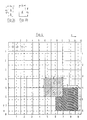
- a picture element A is shown schematically, as is usually used for displaying information on visual display devices.
- This picture element A has a width Ax and a height Ay. These two dimensions correspond, so that the picture element A is square and the width and height form the ratio 1: 1.
- An information element in the form of e.g. round pixel can be displayed.
- a picture element B is shown in dashed lines, which has a width Bx and a height By. If the width and height form the ratio 2: 3, then it is a picture element B, which is used for the information display on a screen text display device. In this case, e.g. elliptical pixel can be displayed.
- Fig. 2 shows an enlarged section of the screen of a data display device.
- This section contains 16 columns in the x direction and 16 rows of square picture elements in the y direction, which have the size of the picture element A shown in FIG. 1a and are shown with solid lines.
- This screen section could also contain 9 columns and 6 rows of such picture elements which correspond to picture element B shown in FIG. 1b.
- This arrangement of picture elements is shown in Fig. 2 by dashed lines, which are numbered accordingly.
- FIG. 2 in the lower right part of the screen section, a square with the side length Q is shown, which is composed of 6 rectangular picture elements a to f, each of which corresponds to picture element B according to FIG. 1b.
- This square would appear on a screen text display device as a representation of 6 screen text pixels, that is, would represent 6 information elements. If these information elements were displayed on a data display device, they would occupy a rectangle that is composed of square picture elements a 'to f' on the screen section in FIG. 2. From the different shape of the two areas occupied by 6 information elements on the screen section, it can be seen that when displaying screen text information on data display devices, a screen text object is reduced in size in the x and y directions, that is to say distorted.
- FIG. 2 an extension of the picture elements A of the data display device in the x direction and in the y direction must be provided , which corresponds to the differences in the dimensions of the picture elements A and B (FIG. 1).
- FIG. 2 can be seen that an object of the screen text, the top left corner of the x, y address 6.4 would appear shifted to the top left on a data display device if it were displayed with the same address but with picture elements of a data display device.
- Fig. 3 shows a type of change of the picture element A of a data display device, by means of which it is possible to display screen text information on a data display device not as true to area but as area-like, ie with similar distortion in the x and y directions, so that only the Scale, but not the form of information to be displayed changes.
- Fig. 3a shows a picture element which is composed of two picture elements A of the type shown in Fig. 1a, so that width and height form the ratio 1: 2.
- Fig. 3b shows a picture element A ', which has been created by widening the picture element according to Fig. 3a and has the width A'x and the height A'y.
- the invention provides the mapping of screen text information with picture elements of this type.
- a picture element A ' can be generated on a data display device in that the pixel in question is displayed twice over one another. The pixels of a picture line are therefore to be reproduced twice below one another. If each pixel then widened in the x direction is, a picture element is filled with the information of each pixel, which corresponds to the picture element A 'of Fig. 3b.
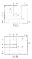
- FIG. 4 An image section of a visual display device is again shown, which has the size of the image section shown in FIG. 2 and contains the square with the side length Q, which consists of the picture elements a to f.
- the upper left corner of this square has the x, y address 6.4 in the dashed grid of picture elements which correspond to picture element B according to FIG. 1b.
- Fig. 4 shows another square with the side length Q ', the upper left corner in the solid line also has the x, y address 6.4 and consists of picture elements a ⁇ to f ⁇ , each of which in Fig. 3b shown picture element A 'correspond.
- Fig. 4 shows that when this principle is used, a screen text object is reproduced in a geometrically similar manner on a data display device, the shift to the top left being significantly less than according to Fig. 2 and a reduction taking place which is only recognizable when the screen size matches, however is also portable.
- FIG. 5 shows a circuit arrangement with which it is possible to optionally display normal data information or screen text information on a data display device.
- This circuit arrangement contains an image information memory 40, into which image information e.g. can be written from the working memory of a data processing device, not shown.
- This image information e.g. the intensity and the color of picture elements can be indicated, are passed via a data bus 42 from the picture information memory 40 to a converter 43, which converts them into analog red-green-blue signals for controlling a screen 44.
- the vertical and horizontal synchronization circuits required to display such information are not shown in FIG. 5. However, it should be assumed that the refresh rate and thus the vertical and horizontal synchronization frequency are constant regardless of the information to be displayed.
- a column counter 46 and a line counter 52 are used to address the image information memory 40.
- the column counter 46 thus addresses the image information memory 40 in the x direction, and the corresponding address signals are fed to it via an address bus 45. They are also fed via this address bus 45 to two comparators 47 and 48 which compare the respective current address with predetermined values X and X '.
- the two comparators 47 and 48 each give an output signal when the current address corresponds to the value X or X '. This output signal is fed via a changeover switch 49 to the reset input R of the column counter 46, the one contact of a changeover switch 51 and the clock input of a D flip-flop 50.
- the column counter 46 By connecting the output signal of the comparators 47 and 48 to the reset input R of the column counter 46, the maximum possible number of picture elements per line is determined in which 44 picture information is displayed on the screen can be displayed. After this maximum value has been reached, the column counter 46 begins its counting process starting from the count value zero. This counting process is controlled with a frequency f1, which is fed to the clock input of the column counter 46 via a changeover switch 57.
- the changeover switch 57 like the changeover switches 49 and 51, is controlled by a control signal U which is supplied to them by the data processing device, not shown.
- the D flip-flop 50 is connected as a factor of two because its data input is connected to its inverting output Q. The signals fed to him at the clock input thus appear at the other contact of the switch 51 with half the frequency.
- the changeover switch 51 is connected to the clock input of the line counter 52, so that it is clocked with the output signals of the D flip-flop 50 when the changeover switch 51 is in the appropriate position. This means that it increases its count by the value 1 every or every second reset of the column counter 46, which depends on the position of the switch 51.
- the output of the line counter 52 like the output of the column counter 46, is connected via an address bus 53 to the image information memory 40 and two comparators 54 and 55.
- the image information memory 40 is addressed in the y direction, the line counter 52 being reset each time the comparator 54 signals that the number of lines Y has been reached or that the comparator 55 signals that the number of lines Y 'has been reached and this signal is sent via a switch 56 to the Reset input of the line counter 52 outputs.
- the switch 56 is also controlled by the control signal U from the data processing device, not shown.
- the switches 49, 51, 56 and 57 must be brought into their second position, for which the control signal U is used. In this position, the readout speed is determined by the frequency f2, which forms the ratio 3: 4 with the frequency f1. It therefore leads to a slower reading of the image information and thus to its extension in the x direction by a factor of 4/3 compared to the previous representation. The readout speed in the y direction is reduced by a factor of 2 by the D flip-flop 50. Since, according to the prerequisite, the horizontal and vertical synchronization of the screen 44 should be constant, the image information of one line is reproduced again in the next line by the switchover.
- the two comparators 48 and 55 determine the resetting of the column counter 46 and the row counter 52 each when the count X 'and Y' is reached. The size of these values must be explained below with reference to FIG. 6.
- the counting volumes 615 and 308 result from the fact that the picture elements of the screen 44 as required by a factor of 4/3 in are widened in the x direction and should assume twice the height in the y direction. Then the screen 44 can only take 615 image elements in the x direction and 308 image elements in the y direction. However, since the screen text information is displayed in accordance with the standard with 480 pixels in the x direction and 240 lines in the y direction, the screen 44 of the data display device cannot be used completely to display a screen text image. The unused area is shown hatched in FIG. 6b.
- the image information store 40 should also have predetermined information for the hatched area, e.g. a constant color reproduction, since the reading of information is basically not interrupted during the addressing of the image information memory 40.
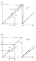
- FIG. 7 shows a diagram of the time course of the addressing of the column counter 46 (FIG. 5) in the x direction.
- the curve 20 shows the increase in the count of the column counter 46 starting from zero to the final value X, which is reached at the time Ts.
- the dashed line 21 correspondingly shows the count of the column counter 46 starting from zero to the end value X ', which is also reached at time Ts.
- the slopes of the two curves 20 and 21 correspond to the timing of the column counter 46 with the frequency f1 or f2. After the time Ts, the counting process for the column counter 46 starts again from the zero count.
- the counting process must be slowed down during the time which corresponds to the width of the different picture part.
- a dash-dotted curve 22 is shown in FIG. 7, which illustrates that the column counter 46 is clocked more slowly during the time tx and, as the time tx elapses, reaches a lower count than in the normal curve 20. Starting from this lower count the column counter 46 is then clocked again faster.
- the dash-dotted curve 23 continued in FIG. 7, it can only reach the final position Xe at the time Ts.
- the column counter 46 When the counting process is continued, the column counter 46 only reaches the final value X corresponding to its counting volume at a later time Te, at which the scanning beam of the screen can already be in the next line.
- X-Xe which for the respective size within of a larger image to be displayed must be determined separately from the ratio tx: Ts in order to carry out a corresponding correction when addressing the image information memory 40 (FIG. 5).
- a more problematic is a correction of the displacement in the x-direction, which a pixel P, which would normally be shown at a certain point on the screen according to the course 20, experiences through the changed course 23.
- the pixel P is represented as the wrong pixel P 'at a later point in time, that is to say shifted in the x direction.
- Information with a column address that has a value greater than Xe can no longer be displayed.
- FIG. 8 shows the course of the addressing of two image information memories in the x-direction, which is composed of the individual courses 20 and 21 already shown in FIG. 7, so that a jump from course 20 into course 21 occurs during time tx results, which corresponds to section 24 of the overall curve.
- this section 24 is switched over and thus from one to the other image information memory, when the time tx has elapsed the system switches back to the first image information memory.
- a time window or an area is opened when displayed on the screen of a visual display device, on which another image with image elements A '(FIG. 1a) within an image with image elements A (FIG. 1a) (FIG. 3b) can be represented.
- Such a representation is shown in Fig. 9a.
- This representation corresponds to that according to Fig. 6b, i.e.
- a complete image 31 could be reproduced on the image area 30 of a data display device, e.g. is a screen text image.
- a part 32 of this screen text image is now mapped within the limits determined by the counter readings Xa, Xb, Ya and Yb described.
- FIG. 9a Another part 33 of the screen text image is indicated by dash-dotted lines in FIG. 9a. If this partial image 33 is to be displayed at the location of the screen area 30 at which the partial image 32 is also displayed, this can be achieved by shifting the entire screen text image 31, as shown in FIG. 9b. This shift results from the offset of the zero points of those counters which address the image information memory containing the screen text image. If the corresponding column counter is reset with a delay of Xr, the respective first pixel of a row is read from the image information memory with a corresponding delay. At this time, however, the scanning beam is at a position corresponding to the address Xr shown in Fig. 9b. A corresponding shift in the y direction can be provided with the amount Yr.
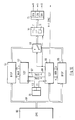
- FIG. 10 shows a circuit arrangement which enables the mode of operation according to FIGS. 8 and 9 and works with two image information memories.
- a data processing device 60 supplies, via an address data bus 61, image information which is to be reproduced with picture elements A '(FIG. 3b) into a first image information memory 62.
- the image information memory 62 is addressed by a column row counter 63 in the x and y directions .
- the clock input of the column line counter 63 is controlled by a clock generator 64, which supplies the clock frequency f2.
- the column row counter 66 synchronizes the column row counter 63 via two outputs 67 and 68 in the x and y directions.
- the output signals of the two image information memories 62 and 65 are fed via a changeover switch 69 to a color table memory 70, which in each case contains a conversion table 71 or 72 for the image information from the image information memory 62 or 65. This converts the image information into digital values for the individual colors red, green and implemented in blue. These values are then fed to a digital / analog conversion circuit 73, which converts the digital values for each color into corresponding analog values. These signals are then fed to the screen. Furthermore, a horizontal-vertical synchronization signal is supplied to the screen, which is emitted by the column row counter 66.
- the column row counter 66 also controls the changeover switch 69 and the color table memory 70.
- This changeover has the advantage that a common memory device and a common digital / analog converter circuit can be used for both color tables 71 and 72.
- the column line counter 63 is shown in the upper part of the figure, and the column line counter 66 is shown in the lower part.
- the column row counter 63 contains a first column counter 75, the clock input of which is controlled by the clock signals of the frequency f2.
- the output signals of the first column counter 75 are fed to a comparator 76 and to the image information memory 62. If the output signals correspond to a predetermined count X ', the comparator 76 outputs a reset signal via an OR gate 77 to the reset input of the column counter 75.
- the OR gate 77 is also driven with the x synchronization signal from the column row counter 66.
- the output of the comparator 76 is connected to a D flip-flop 78, which is connected as a factor of two. Its inverting output Q is connected to the clock input of a first line counter 79. Like the column counter 75, this is connected to a comparator 80 which, when a predetermined count Y 'is reached, outputs an output signal via an OR gate 81 to the reset input of the line counter 79. The output signals of the line counter 79 are also output to the image information memory 62.
- the OR gate 81 is driven at its second input by the y synchronization signal from the column row counter 66.
- the column row counter 66 contains a second column counter 85, the clock input of which is supplied with the clock signals with the frequency f1.
- the output of the column counter 85 is connected to the image information memory 65 and to the first inputs of comparators 86, 87, 88, 89.
- the comparators 87, 88, 89 are connected at their second inputs to the address data bus 61 and receive the values Xr, Xa and Xb via them (FIGS. 8, 9).
- the comparison value X of the comparator 86 is fixed.
- the output of this comparator 86 is connected to the reset input of the column counter 85 and to the clock input of a second row counter 90.
- the output of the comparator 87 provides the x synchronization signal.
- the outputs of the comparators 88 and 89 are connected to the two inputs of an AND gate 91, the output of which controls the one input of a further AND gate 92.
- the output of the line counter 90 is connected to the inputs of comparators 93, 94, 95, 96. These comparators are connected similarly to the comparators 86, 87, 88, 89 and are used to derive the corresponding y signals and the second input signal for the AND gate 92 via one AND gate 97.
- the comparators 94, 95, 96 also receive their second input signals via the address data bus 61.
- the output of the line counter 90 supplies its signals for the y direction to the image information memory 65.
- the AND gate 92 supplies the control signal for the changeover switch 69 and the color table memory 70.
- the operation of the column row counter 63 can be understood on the basis of the functional description of the circuit arrangement shown in FIG. 5. The same applies to the mode of operation of column row counter 66 insofar as column counter 85 with comparator 86 and row counter 90 with comparator 93 are concerned.
- the interaction of the two column row counters 63 and 66 corresponds to the procedure described with reference to FIGS. 8 and 9.
- the column counter 85 reaches the count X, it is reset.
- the x synchronization signal is output to the column row counter 63 and its column counter 75 is reset. If the count is between the values Xa and Xb, the comparators 88 and 89 deliver a logic 1 signal, and the AND gate 91 is switched through.
Landscapes
- Engineering & Computer Science (AREA)
- Physics & Mathematics (AREA)
- Computer Hardware Design (AREA)
- General Physics & Mathematics (AREA)
- Theoretical Computer Science (AREA)
- Multimedia (AREA)
- Signal Processing (AREA)
- Controls And Circuits For Display Device (AREA)
Applications Claiming Priority (2)
| Application Number | Priority Date | Filing Date | Title |
|---|---|---|---|
| DE3808668 | 1988-03-15 | ||
| DE3808668A DE3808668C1 (zh) | 1988-03-15 | 1988-03-15 |
Publications (3)
| Publication Number | Publication Date |
|---|---|
| EP0337104A2 EP0337104A2 (de) | 1989-10-18 |
| EP0337104A3 EP0337104A3 (en) | 1989-10-25 |
| EP0337104B1 true EP0337104B1 (de) | 1994-06-15 |
Family
ID=6349809
Family Applications (1)
| Application Number | Title | Priority Date | Filing Date |
|---|---|---|---|
| EP89103930A Expired - Lifetime EP0337104B1 (de) | 1988-03-15 | 1989-03-06 | Schaltungsanordnung zum Steuern der bildlichen rasterartigen Darstellung von Informationen |
Country Status (3)
| Country | Link |
|---|---|
| US (1) | US5319383A (zh) |
| EP (1) | EP0337104B1 (zh) |
| DE (2) | DE3808668C1 (zh) |
Families Citing this family (5)
| Publication number | Priority date | Publication date | Assignee | Title |
|---|---|---|---|---|
| JPH05502568A (ja) * | 1990-09-19 | 1993-04-28 | エヌ ベー フィリップス フルーイランペンファブリケン | 読取り装置 |
| NL9002114A (nl) * | 1990-09-19 | 1992-04-16 | Koninkl Philips Electronics Nv | Beeldopslagsysteem. |
| US5400051A (en) * | 1992-11-12 | 1995-03-21 | International Business Machines Corporation | Method and system for generating variably scaled digital images |
| EP0644684B1 (en) * | 1993-09-17 | 2000-02-02 | Eastman Kodak Company | Digital resampling integrated circuit for fast image resizing applications |
| US6178272B1 (en) * | 1999-02-02 | 2001-01-23 | Oplus Technologies Ltd. | Non-linear and linear method of scale-up or scale-down image resolution conversion |
Family Cites Families (17)
| Publication number | Priority date | Publication date | Assignee | Title |
|---|---|---|---|---|
| FR2430850A1 (fr) * | 1978-07-14 | 1980-02-08 | Information Int Inc | Systeme de photocomposition fournissant une copie tramee d'une image d'origine, et procede d'obtention d'une copie tramee |
| GB2085257B (en) * | 1980-09-03 | 1984-09-12 | Nat Res Dev | Apparatus and methods for varying the format of a raster scan display |
| GB2100097B (en) * | 1981-06-03 | 1984-12-05 | Jpm Automatic Machines Ltd | Improvements relating to video display systems |
| US4610026A (en) * | 1982-04-30 | 1986-09-02 | Hitachi, Ltd. | Method of and apparatus for enlarging/reducing two-dimensional images |
| DE3228102A1 (de) * | 1982-07-28 | 1984-02-02 | Licentia Patent-Verwaltungs-Gmbh, 6000 Frankfurt | Sichtgeraet mit einer kathodenstrahlroehre |
| NL8204728A (nl) * | 1982-12-07 | 1984-07-02 | Philips Nv | Televisieschakeling voor raster- en lijnfrekwentieverdubbeling en beelddeelvergroting. |
| DE3318658A1 (de) * | 1983-05-21 | 1984-11-22 | Robert Bosch Gmbh, 7000 Stuttgart | Verfahren zur fernsehmaessigen abtastung von filmen |
| JPH0744641B2 (ja) * | 1983-06-06 | 1995-05-15 | キヤノン株式会社 | 画像変倍処理装置 |
| JPS6061796A (ja) * | 1983-09-16 | 1985-04-09 | シャープ株式会社 | 表示装置 |
| JPS60169893A (ja) * | 1984-02-15 | 1985-09-03 | シチズン時計株式会社 | ビツトパタ−ン変換装置 |
| JPH0652472B2 (ja) * | 1984-07-23 | 1994-07-06 | インターナショナル・ビジネス・マシーンズ・コーポレーション | イメージ処理方法 |
| US4724446A (en) * | 1985-01-31 | 1988-02-09 | Kabushiki Kaisha Toshiba | Thermal transfer printing apparatus |
| US4875173A (en) * | 1985-04-16 | 1989-10-17 | Minolta Camera Kabushiki Kaisha | Image enlarging method and device |
| GB2180128B (en) * | 1985-08-28 | 1990-01-10 | Anamartic Ltd | Window graphics system |
| US4680645A (en) * | 1986-08-25 | 1987-07-14 | Hewlett-Packard Company | Method for rendering gray scale images with variable dot sizes |
| DE3722172A1 (de) * | 1987-07-04 | 1989-01-12 | Thomson Brandt Gmbh | Verfahren und vorrichtung zur ausschnittvergroesserung eines fernsehbildes |
| US4821031A (en) * | 1988-01-20 | 1989-04-11 | International Computers Limited | Image display apparatus |
-
1988
- 1988-03-15 DE DE3808668A patent/DE3808668C1/de not_active Expired
-
1989
- 1989-03-06 DE DE58907871T patent/DE58907871D1/de not_active Expired - Fee Related
- 1989-03-06 EP EP89103930A patent/EP0337104B1/de not_active Expired - Lifetime
-
1992
- 1992-01-03 US US07/816,788 patent/US5319383A/en not_active Expired - Fee Related
Also Published As
| Publication number | Publication date |
|---|---|
| EP0337104A2 (de) | 1989-10-18 |
| DE58907871D1 (de) | 1994-07-21 |
| EP0337104A3 (en) | 1989-10-25 |
| DE3808668C1 (zh) | 1989-06-22 |
| US5319383A (en) | 1994-06-07 |
Similar Documents
| Publication | Publication Date | Title |
|---|---|---|
| DE2950712C2 (de) | Einrichtung zur Erzeugung eines elektronischen Hintergrundrasters | |
| DE4332573C2 (de) | Videographiksystem zum Anzeigen von Signalverläufen auf einem Videomonitor | |
| DE3702220C2 (zh) | ||
| DE68928773T2 (de) | Verfahren zum senkrechten Filtern bei rasterabgetasteten Anzeigevorrichtungen | |
| DE3619019C2 (de) | Digitale Konvergenzkorrekturvorrichtung | |
| DE2156423C3 (zh) | ||
| DE69033156T2 (de) | Bildschirmanzeige an einem Fernsehempfänger | |
| DE2735213B2 (de) | Gerät zum Steuern der Bilddarstellung bei einem Farbfernsehgerät | |
| DE2063243C3 (de) | Einrichtung zur farbigen Wiedergabe von Bildzeilen auf einem Bildschirm eines Datensichtgerätes | |
| DE2622869B2 (de) | Anordnung zur Erzeugung von Zeichen zur Einblendung in das von einem Fernsehgerät dargestellte Bild | |
| DE3022118C2 (de) | Ansteuerschaltung für ein Zeichen/Graphik-Anzeigegerät | |
| DE2510542A1 (de) | Digitale bildwiedergabevorrichtung mit mehreren bildschirmen | |
| DE2223332B2 (de) | Einrichtung zur sichtbaren Anzeige von Daten auf einem Wiedergabegerät | |
| DE69229033T2 (de) | Bildverarbeitungssystem | |
| DE2438203A1 (de) | Anzeigeeinrichtung | |
| DE3823921A1 (de) | Verfahren und geraet zum speichern digitaler videosignale | |
| EP0337104B1 (de) | Schaltungsanordnung zum Steuern der bildlichen rasterartigen Darstellung von Informationen | |
| DE2741161A1 (de) | Anzeige-system | |
| DE3624191C2 (zh) | ||
| DE69123319T2 (de) | Bilddatenverarbeitungsgerät | |
| DE2920228A1 (de) | Signalgenerator fuer schreiber- datenstation | |
| DE2350018B2 (de) | Bildanalysator | |
| DE3206565A1 (de) | Steueranordnung fuer ein datensichtgeraet | |
| DE2439102A1 (de) | Verfahren zum darstellen von bildern in form von digitalen daten | |
| EP0598434B1 (de) | Verfahren und Schaltungsanordnung zum Darstellen von Zeichen mit Umrandung |
Legal Events
| Date | Code | Title | Description |
|---|---|---|---|
| PUAI | Public reference made under article 153(3) epc to a published international application that has entered the european phase |
Free format text: ORIGINAL CODE: 0009012 |
|
| PUAL | Search report despatched |
Free format text: ORIGINAL CODE: 0009013 |
|
| AK | Designated contracting states |
Kind code of ref document: A2 Designated state(s): AT BE CH DE ES FR GB GR IT LI LU NL SE |
|
| AK | Designated contracting states |
Kind code of ref document: A3 Designated state(s): AT BE CH DE ES FR GB GR IT LI LU NL SE |
|
| 17P | Request for examination filed |
Effective date: 19890927 |
|
| RBV | Designated contracting states (corrected) |
Designated state(s): DE FR GB IT NL SE |
|
| RAP3 | Party data changed (applicant data changed or rights of an application transferred) |
Owner name: SIEMENS NIXDORF INFORMATIONSSYSTEME AKTIENGESELLSC |
|
| 17Q | First examination report despatched |
Effective date: 19920728 |
|
| GRAA | (expected) grant |
Free format text: ORIGINAL CODE: 0009210 |
|
| AK | Designated contracting states |
Kind code of ref document: B1 Designated state(s): DE FR GB IT NL SE |
|
| PG25 | Lapsed in a contracting state [announced via postgrant information from national office to epo] |
Ref country code: IT Free format text: LAPSE BECAUSE OF FAILURE TO SUBMIT A TRANSLATION OF THE DESCRIPTION OR TO PAY THE FEE WITHIN THE PRE;WARNING: LAPSES OF ITALIAN PATENTS WITH EFFECTIVE DATE BEFORE 2007 MAY HAVE OCCURRED AT ANY TIME BEFORE 2007. THE CORRECT EFFECTIVE DATE MAY BE DIFFERENT FROM THE ONE RECORDED.SCRIBED TIME-LIMIT Effective date: 19940615 Ref country code: FR Free format text: THE PATENT HAS BEEN ANNULLED BY A DECISION OF A NATIONAL AUTHORITY Effective date: 19940615 Ref country code: NL Effective date: 19940615 |
|
| REF | Corresponds to: |
Ref document number: 58907871 Country of ref document: DE Date of ref document: 19940721 |
|
| PG25 | Lapsed in a contracting state [announced via postgrant information from national office to epo] |
Ref country code: SE Effective date: 19940915 |
|
| GBT | Gb: translation of ep patent filed (gb section 77(6)(a)/1977) |
Effective date: 19940822 |
|
| ET | Fr: translation filed | ||
| NLV1 | Nl: lapsed or annulled due to failure to fulfill the requirements of art. 29p and 29m of the patents act | ||
| PG25 | Lapsed in a contracting state [announced via postgrant information from national office to epo] |
Ref country code: GB Effective date: 19950306 |
|
| PLBE | No opposition filed within time limit |
Free format text: ORIGINAL CODE: 0009261 |
|
| STAA | Information on the status of an ep patent application or granted ep patent |
Free format text: STATUS: NO OPPOSITION FILED WITHIN TIME LIMIT |
|
| 26N | No opposition filed | ||
| PGFP | Annual fee paid to national office [announced via postgrant information from national office to epo] |
Ref country code: DE Payment date: 19950621 Year of fee payment: 7 |
|
| GBPC | Gb: european patent ceased through non-payment of renewal fee |
Effective date: 19950306 |
|
| REG | Reference to a national code |
Ref country code: FR Ref legal event code: ST |
|
| PG25 | Lapsed in a contracting state [announced via postgrant information from national office to epo] |
Ref country code: DE Effective date: 19961203 |