EP0336497A1 - Verfahren zum Herstellen eines Chipwiderstandes - Google Patents
Verfahren zum Herstellen eines Chipwiderstandes Download PDFInfo
- Publication number
- EP0336497A1 EP0336497A1 EP89200806A EP89200806A EP0336497A1 EP 0336497 A1 EP0336497 A1 EP 0336497A1 EP 89200806 A EP89200806 A EP 89200806A EP 89200806 A EP89200806 A EP 89200806A EP 0336497 A1 EP0336497 A1 EP 0336497A1
- Authority
- EP
- European Patent Office
- Prior art keywords
- strips
- layers
- resistor body
- electrically insulating
- electrically
- Prior art date
- Legal status (The legal status is an assumption and is not a legal conclusion. Google has not performed a legal analysis and makes no representation as to the accuracy of the status listed.)
- Granted
Links
Images
Classifications
-
- H—ELECTRICITY
- H01—ELECTRIC ELEMENTS
- H01C—RESISTORS
- H01C7/00—Non-adjustable resistors formed as one or more layers or coatings; Non-adjustable resistors made from powdered conducting material or powdered semi-conducting material with or without insulating material
-
- H—ELECTRICITY
- H01—ELECTRIC ELEMENTS
- H01C—RESISTORS
- H01C17/00—Apparatus or processes specially adapted for manufacturing resistors
- H01C17/006—Apparatus or processes specially adapted for manufacturing resistors adapted for manufacturing resistor chips
-
- H—ELECTRICITY
- H01—ELECTRIC ELEMENTS
- H01C—RESISTORS
- H01C13/00—Resistors not provided for elsewhere
- H01C13/02—Structural combinations of resistors
Definitions
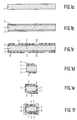
- a plate of ceramic resistance material is provided on both sides with electrically conductive layers, - both sides of the plate are provided with electrically insulating layers according to a pattern, - the plate is divided into strips, - the strips are provided on the large uninsulated sides with electrically insulating strips, - the strips are provided with solderable metal strips on top of the electrically insulating strips, each of the metal strips being electrically conductively connected to one of the electrically conductive layers, - the strips are divided into cuboids.
Priority Applications (1)
| Application Number | Priority Date | Filing Date | Title |
|---|---|---|---|
| AT89200806T ATE100627T1 (de) | 1988-04-05 | 1989-03-30 | Verfahren zum herstellen eines chipwiderstandes. |
Applications Claiming Priority (2)
| Application Number | Priority Date | Filing Date | Title |
|---|---|---|---|
| NL8800853 | 1988-04-05 | ||
| NL8800853A NL8800853A (nl) | 1988-04-05 | 1988-04-05 | Chipweerstand en werkwijze voor het vervaardigen van een chipweerstand. |
Publications (2)
| Publication Number | Publication Date |
|---|---|
| EP0336497A1 true EP0336497A1 (de) | 1989-10-11 |
| EP0336497B1 EP0336497B1 (de) | 1994-01-19 |
Family
ID=19852059
Family Applications (1)
| Application Number | Title | Priority Date | Filing Date |
|---|---|---|---|
| EP89200806A Expired - Lifetime EP0336497B1 (de) | 1988-04-05 | 1989-03-30 | Verfahren zum Herstellen eines Chipwiderstandes |
Country Status (7)
| Country | Link |
|---|---|
| US (1) | US4992771A (de) |
| EP (1) | EP0336497B1 (de) |
| JP (1) | JPH01302803A (de) |
| KR (1) | KR890016588A (de) |
| AT (1) | ATE100627T1 (de) |
| DE (1) | DE68912379T2 (de) |
| NL (1) | NL8800853A (de) |
Cited By (3)
| Publication number | Priority date | Publication date | Assignee | Title |
|---|---|---|---|---|
| EP0790625A2 (de) * | 1996-02-13 | 1997-08-20 | Daito Communication Apparatus Co. Ltd. | PTC-Element |
| EP1041586A2 (de) * | 1999-04-01 | 2000-10-04 | Murata Manufacturing Co., Ltd. | Thermsitorchip |
| EP2680279A1 (de) * | 2012-06-25 | 2014-01-01 | Ralec Electronic Corporation | Verfahren zur Herstellung eines SMD Widerstands |
Families Citing this family (26)
| Publication number | Priority date | Publication date | Assignee | Title |
|---|---|---|---|---|
| FR2653588B1 (fr) * | 1989-10-20 | 1992-02-07 | Electro Resistance | Resistance electrique sous forme de puce a montage de surface et son procede de fabrication. |
| JPH04111701U (ja) * | 1991-03-13 | 1992-09-29 | 株式会社村田製作所 | 電信電話用端末装置 |
| JPH076902A (ja) * | 1991-03-13 | 1995-01-10 | Murata Mfg Co Ltd | 正特性サーミスタ素子 |
| US5257003A (en) * | 1992-01-14 | 1993-10-26 | Mahoney John J | Thermistor and its method of manufacture |
| US5852397A (en) | 1992-07-09 | 1998-12-22 | Raychem Corporation | Electrical devices |
| US5339068A (en) * | 1992-12-18 | 1994-08-16 | Mitsubishi Materials Corp. | Conductive chip-type ceramic element and method of manufacture thereof |
| US5808893A (en) * | 1993-07-28 | 1998-09-15 | Amt Machine Systems, Ltd. | System for adapting an automatic screw machine to achieve computer numeric control |
| WO1995008176A1 (en) * | 1993-09-15 | 1995-03-23 | Raychem Corporation | Electrical assembly comprising a ptc resistive element |
| US5379017A (en) * | 1993-10-25 | 1995-01-03 | Rohm Co., Ltd. | Square chip resistor |
| WO1995031816A1 (en) * | 1994-05-16 | 1995-11-23 | Raychem Corporation | Electrical devices comprising a ptc resistive element |
| EP0766867B1 (de) * | 1994-06-09 | 2002-11-20 | Tyco Electronics Corporation | Elektrische bauelemente |
| US5907272A (en) * | 1996-01-22 | 1999-05-25 | Littelfuse, Inc. | Surface mountable electrical device comprising a PTC element and a fusible link |
| US5900800A (en) * | 1996-01-22 | 1999-05-04 | Littelfuse, Inc. | Surface mountable electrical device comprising a PTC element |
| US6023403A (en) * | 1996-05-03 | 2000-02-08 | Littlefuse, Inc. | Surface mountable electrical device comprising a PTC and fusible element |
| JP3609551B2 (ja) * | 1996-08-08 | 2005-01-12 | アスモ株式会社 | サーミスタ |
| US6838972B1 (en) * | 1999-02-22 | 2005-01-04 | Littelfuse, Inc. | PTC circuit protection devices |
| US6854176B2 (en) * | 1999-09-14 | 2005-02-15 | Tyco Electronics Corporation | Process for manufacturing a composite polymeric circuit protection device |
| US6640420B1 (en) | 1999-09-14 | 2003-11-04 | Tyco Electronics Corporation | Process for manufacturing a composite polymeric circuit protection device |
| TWM285123U (en) * | 2005-05-26 | 2006-01-01 | Inpaq Technology Co Ltd | Chip-type resettable over-current protection device structure |
| US7576508B2 (en) * | 2003-01-30 | 2009-08-18 | Honeywell International Inc. | Gas turbine engine starter generator with AC generator and DC motor modes |
| US7026583B2 (en) * | 2004-04-05 | 2006-04-11 | China Steel Corporation | Surface mountable PTC device |
| US20050258167A1 (en) * | 2004-05-24 | 2005-11-24 | Tony Cheng | Electrical heating device |
| US20060132277A1 (en) * | 2004-12-22 | 2006-06-22 | Tyco Electronics Corporation | Electrical devices and process for making such devices |
| US8546818B2 (en) | 2007-06-12 | 2013-10-01 | SemiLEDs Optoelectronics Co., Ltd. | Vertical LED with current-guiding structure |
| US20090027821A1 (en) * | 2007-07-26 | 2009-01-29 | Littelfuse, Inc. | Integrated thermistor and metallic element device and method |
| US8584348B2 (en) * | 2011-03-05 | 2013-11-19 | Weis Innovations | Method of making a surface coated electronic ceramic component |
Citations (4)
| Publication number | Priority date | Publication date | Assignee | Title |
|---|---|---|---|---|
| GB1188213A (en) * | 1967-03-17 | 1970-04-15 | Power Dev Ltd | Improvements in Resistor Elements |
| DE3148778A1 (de) * | 1981-05-21 | 1982-12-09 | Resista Fabrik elektrischer Widerstände GmbH, 8300 Landshut | Bauelemente in chip-bauweise und verfahren zu dessen herstellung |
| EP0229286A1 (de) * | 1985-12-17 | 1987-07-22 | Siemens Aktiengesellschaft | Elektrisches Bauelement in Chip-Bauweise |
| US4706060A (en) * | 1986-09-26 | 1987-11-10 | General Electric Company | Surface mount varistor |
-
1988
- 1988-04-05 NL NL8800853A patent/NL8800853A/nl not_active Application Discontinuation
-
1989
- 1989-03-30 EP EP89200806A patent/EP0336497B1/de not_active Expired - Lifetime
- 1989-03-30 DE DE68912379T patent/DE68912379T2/de not_active Expired - Fee Related
- 1989-03-30 AT AT89200806T patent/ATE100627T1/de not_active IP Right Cessation
- 1989-04-03 KR KR1019890004345A patent/KR890016588A/ko not_active Application Discontinuation
- 1989-04-03 JP JP1081647A patent/JPH01302803A/ja active Pending
- 1989-04-05 US US07/333,483 patent/US4992771A/en not_active Expired - Fee Related
Patent Citations (4)
| Publication number | Priority date | Publication date | Assignee | Title |
|---|---|---|---|---|
| GB1188213A (en) * | 1967-03-17 | 1970-04-15 | Power Dev Ltd | Improvements in Resistor Elements |
| DE3148778A1 (de) * | 1981-05-21 | 1982-12-09 | Resista Fabrik elektrischer Widerstände GmbH, 8300 Landshut | Bauelemente in chip-bauweise und verfahren zu dessen herstellung |
| EP0229286A1 (de) * | 1985-12-17 | 1987-07-22 | Siemens Aktiengesellschaft | Elektrisches Bauelement in Chip-Bauweise |
| US4706060A (en) * | 1986-09-26 | 1987-11-10 | General Electric Company | Surface mount varistor |
Cited By (5)
| Publication number | Priority date | Publication date | Assignee | Title |
|---|---|---|---|---|
| EP0790625A2 (de) * | 1996-02-13 | 1997-08-20 | Daito Communication Apparatus Co. Ltd. | PTC-Element |
| EP0790625A3 (de) * | 1996-02-13 | 1998-07-29 | Daito Communication Apparatus Co. Ltd. | PTC-Element |
| EP1041586A2 (de) * | 1999-04-01 | 2000-10-04 | Murata Manufacturing Co., Ltd. | Thermsitorchip |
| EP1041586A3 (de) * | 1999-04-01 | 2004-01-02 | Murata Manufacturing Co., Ltd. | Thermsitorchip |
| EP2680279A1 (de) * | 2012-06-25 | 2014-01-01 | Ralec Electronic Corporation | Verfahren zur Herstellung eines SMD Widerstands |
Also Published As
| Publication number | Publication date |
|---|---|
| EP0336497B1 (de) | 1994-01-19 |
| JPH01302803A (ja) | 1989-12-06 |
| NL8800853A (nl) | 1989-11-01 |
| DE68912379T2 (de) | 1994-07-28 |
| KR890016588A (ko) | 1989-11-29 |
| DE68912379D1 (de) | 1994-03-03 |
| US4992771A (en) | 1991-02-12 |
| ATE100627T1 (de) | 1994-02-15 |
Similar Documents
| Publication | Publication Date | Title |
|---|---|---|
| EP0336497B1 (de) | Verfahren zum Herstellen eines Chipwiderstandes | |
| KR910000969B1 (ko) | 칩형 저항기 | |
| JP2726130B2 (ja) | 金属有機物膜からなる少量アンペア用ヒューズ及びその製造方法 | |
| EP0929083B1 (de) | Widerstand und sein Herstellungsverfahren | |
| EP0326212B1 (de) | Chipwiderstand und Verfahren zum Herstellen eines Chipwiderstandes | |
| JP3147134B2 (ja) | チップ型サーミスタ及びその製造方法 | |
| JP3363295B2 (ja) | チップ電子部品 | |
| KR19980018524A (ko) | 최소한 한 금속-적층을 가진 기판의 제조방법 및 프린트기판과 그의 적용 | |
| JPH09320802A (ja) | 抵抗器 | |
| JP3167968B2 (ja) | チップ抵抗器の製造方法 | |
| JPH0595071U (ja) | 厚膜回路基板 | |
| JPH02224202A (ja) | チップ型固定抵抗器の製造方法 | |
| JP3286855B2 (ja) | チップ型ptcサーミスタの製造方法 | |
| JP3353037B2 (ja) | チップ抵抗器 | |
| JPH0963805A (ja) | 角形チップ抵抗器 | |
| JPS6320081Y2 (de) | ||
| JP2939425B2 (ja) | 表面実装型抵抗器とその製造方法 | |
| JP3165517B2 (ja) | 回路装置 | |
| JPS637601A (ja) | 面実装用ネツトワ−ク抵抗器 | |
| JP2001044068A (ja) | 小型な表面実装用部品及びその製造方法 | |
| EP1619696A2 (de) | Oberflächenmontierbarer Chip-Widerstand und Verfahren zu seiner Herstellung | |
| JP2001167907A (ja) | チップ型サーミスタ及びその製造方法 | |
| US3588974A (en) | Method of manufacturing an electronic component | |
| JP3884085B2 (ja) | 小型寸法の電気的、電子的又は電気機械的な素子の製造方法 | |
| JPH07211509A (ja) | チップ抵抗器とその製造方法 |
Legal Events
| Date | Code | Title | Description |
|---|---|---|---|
| PUAI | Public reference made under article 153(3) epc to a published international application that has entered the european phase |
Free format text: ORIGINAL CODE: 0009012 |
|
| AK | Designated contracting states |
Kind code of ref document: A1 Designated state(s): AT BE DE FR GB NL |
|
| 17P | Request for examination filed |
Effective date: 19900406 |
|
| 17Q | First examination report despatched |
Effective date: 19920609 |
|
| GRAA | (expected) grant |
Free format text: ORIGINAL CODE: 0009210 |
|
| AK | Designated contracting states |
Kind code of ref document: B1 Designated state(s): AT BE DE FR GB NL |
|
| PG25 | Lapsed in a contracting state [announced via postgrant information from national office to epo] |
Ref country code: NL Effective date: 19940119 Ref country code: BE Effective date: 19940119 Ref country code: AT Effective date: 19940119 |
|
| REF | Corresponds to: |
Ref document number: 100627 Country of ref document: AT Date of ref document: 19940215 Kind code of ref document: T |
|
| REF | Corresponds to: |
Ref document number: 68912379 Country of ref document: DE Date of ref document: 19940303 |
|
| ET | Fr: translation filed | ||
| NLV1 | Nl: lapsed or annulled due to failure to fulfill the requirements of art. 29p and 29m of the patents act | ||
| PLBE | No opposition filed within time limit |
Free format text: ORIGINAL CODE: 0009261 |
|
| STAA | Information on the status of an ep patent application or granted ep patent |
Free format text: STATUS: NO OPPOSITION FILED WITHIN TIME LIMIT |
|
| 26N | No opposition filed | ||
| PGFP | Annual fee paid to national office [announced via postgrant information from national office to epo] |
Ref country code: GB Payment date: 19950228 Year of fee payment: 7 |
|
| PGFP | Annual fee paid to national office [announced via postgrant information from national office to epo] |
Ref country code: FR Payment date: 19950329 Year of fee payment: 7 |
|
| PGFP | Annual fee paid to national office [announced via postgrant information from national office to epo] |
Ref country code: DE Payment date: 19950529 Year of fee payment: 7 |
|
| REG | Reference to a national code |
Ref country code: FR Ref legal event code: CD |
|
| PG25 | Lapsed in a contracting state [announced via postgrant information from national office to epo] |
Ref country code: GB Effective date: 19960330 |
|
| GBPC | Gb: european patent ceased through non-payment of renewal fee |
Effective date: 19960330 |
|
| PG25 | Lapsed in a contracting state [announced via postgrant information from national office to epo] |
Ref country code: FR Effective date: 19961129 |
|
| PG25 | Lapsed in a contracting state [announced via postgrant information from national office to epo] |
Ref country code: DE Effective date: 19961203 |
|
| REG | Reference to a national code |
Ref country code: FR Ref legal event code: ST |