EP0336319A2 - MOS SRAM vom internen Synchronisations-Typ mit Detektorschaltung für Adressenumwandlung - Google Patents
MOS SRAM vom internen Synchronisations-Typ mit Detektorschaltung für Adressenumwandlung Download PDFInfo
- Publication number
- EP0336319A2 EP0336319A2 EP89105724A EP89105724A EP0336319A2 EP 0336319 A2 EP0336319 A2 EP 0336319A2 EP 89105724 A EP89105724 A EP 89105724A EP 89105724 A EP89105724 A EP 89105724A EP 0336319 A2 EP0336319 A2 EP 0336319A2
- Authority
- EP
- European Patent Office
- Prior art keywords
- signal
- address
- address transition
- mos transistors
- supplied
- Prior art date
- Legal status (The legal status is an assumption and is not a legal conclusion. Google has not performed a legal analysis and makes no representation as to the accuracy of the status listed.)
- Granted
Links
Images


Classifications
-
- G—PHYSICS
- G11—INFORMATION STORAGE
- G11C—STATIC STORES
- G11C11/00—Digital stores characterised by the use of particular electric or magnetic storage elements; Storage elements therefor
- G11C11/21—Digital stores characterised by the use of particular electric or magnetic storage elements; Storage elements therefor using electric elements
- G11C11/34—Digital stores characterised by the use of particular electric or magnetic storage elements; Storage elements therefor using electric elements using semiconductor devices
-
- G—PHYSICS
- G11—INFORMATION STORAGE
- G11C—STATIC STORES
- G11C8/00—Arrangements for selecting an address in a digital store
- G11C8/18—Address timing or clocking circuits; Address control signal generation or management, e.g. for row address strobe [RAS] or column address strobe [CAS] signals
-
- G—PHYSICS
- G11—INFORMATION STORAGE
- G11C—STATIC STORES
- G11C11/00—Digital stores characterised by the use of particular electric or magnetic storage elements; Storage elements therefor
- G11C11/21—Digital stores characterised by the use of particular electric or magnetic storage elements; Storage elements therefor using electric elements
- G11C11/34—Digital stores characterised by the use of particular electric or magnetic storage elements; Storage elements therefor using electric elements using semiconductor devices
- G11C11/40—Digital stores characterised by the use of particular electric or magnetic storage elements; Storage elements therefor using electric elements using semiconductor devices using transistors
- G11C11/41—Digital stores characterised by the use of particular electric or magnetic storage elements; Storage elements therefor using electric elements using semiconductor devices using transistors forming static cells with positive feedback, i.e. cells not needing refreshing or charge regeneration, e.g. bistable multivibrator or Schmitt trigger
- G11C11/413—Auxiliary circuits, e.g. for addressing, decoding, driving, writing, sensing, timing or power reduction
- G11C11/417—Auxiliary circuits, e.g. for addressing, decoding, driving, writing, sensing, timing or power reduction for memory cells of the field-effect type
- G11C11/418—Address circuits
-
- G—PHYSICS
- G11—INFORMATION STORAGE
- G11C—STATIC STORES
- G11C2207/00—Indexing scheme relating to arrangements for writing information into, or reading information out from, a digital store
- G11C2207/06—Sense amplifier related aspects
- G11C2207/061—Sense amplifier enabled by a address transition detection related control signal
Definitions
- the address transition detecting signal is extended in the write mode by means of the pulse width extension circuit, and a bit line initializing signal having a longer pulse width than that in the readout mode can be generated. That is, the initializing time in the write mode becomes long to delay the inversion of the bit line potential, thus effectively preventing the erroneous data writing operation.
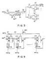
- Each address transition detecting section (ATDL) 19 detects change of row address signals X0, X1, - -- and column address signals Y0, --- and supplies address transition detecting signal ⁇ ATDL .
- Each address transition detecting signal ⁇ ATDL is supplied to address transition detecting circuit (ATD) 20.
- the logical sum of received address transition detecting signals ⁇ ATDL is derived by means of address transition detecting circuit (ATD) 20 and corresponding address transition signal ⁇ ATD is supplied as a monostable pulse.
- Address transition signal ⁇ ATD is supplied to pulse width extension circuit 21.
- the pulse width of address transition signal ⁇ ATD is set to be longer in the write mode than in the readout mode in the same manner as in the circuit of Fig. 3.
Landscapes
- Engineering & Computer Science (AREA)
- Microelectronics & Electronic Packaging (AREA)
- Computer Hardware Design (AREA)
- Static Random-Access Memory (AREA)
Applications Claiming Priority (2)
| Application Number | Priority Date | Filing Date | Title |
|---|---|---|---|
| JP63076606A JPH0766665B2 (ja) | 1988-03-31 | 1988-03-31 | 半導体記憶装置 |
| JP76606/88 | 1988-03-31 |
Publications (3)
| Publication Number | Publication Date |
|---|---|
| EP0336319A2 true EP0336319A2 (de) | 1989-10-11 |
| EP0336319A3 EP0336319A3 (en) | 1990-03-07 |
| EP0336319B1 EP0336319B1 (de) | 1993-09-29 |
Family
ID=13609993
Family Applications (1)
| Application Number | Title | Priority Date | Filing Date |
|---|---|---|---|
| EP89105724A Expired - Lifetime EP0336319B1 (de) | 1988-03-31 | 1989-03-31 | MOS SRAM vom internen Synchronisations-Typ mit Detektorschaltung für Adressenumwandlung |
Country Status (6)
| Country | Link |
|---|---|
| US (1) | US4916668A (de) |
| EP (1) | EP0336319B1 (de) |
| JP (1) | JPH0766665B2 (de) |
| KR (1) | KR920008031B1 (de) |
| DE (1) | DE68909467T2 (de) |
| MY (1) | MY104082A (de) |
Cited By (6)
| Publication number | Priority date | Publication date | Assignee | Title |
|---|---|---|---|---|
| GB2247759A (en) * | 1990-09-04 | 1992-03-11 | Samsung Electronics Co Ltd | Semiconductor memory address decoder with delayed output. |
| AU642978B2 (en) * | 1991-03-12 | 1993-11-04 | Alcatel N.V. | Method and device for aquisition and alignment of data |
| EP0453678B1 (de) * | 1988-10-28 | 1995-01-11 | STERN & STERN INDUSTRIES, INC. | Gewebe mit geringer Durchlässigkeit und Herstellungsweise |
| EP0794618A1 (de) * | 1996-03-06 | 1997-09-10 | STMicroelectronics S.r.l. | Adressenübergangsabfühlschaltung |
| EP0740303A3 (de) * | 1995-04-24 | 1998-12-16 | Nec Corporation | Statische Halbleiterspeicheranordnung mit Impulsgenerator zur Verminderung des Schreibzyklus |
| EP0960421A4 (de) * | 1997-01-24 | 2003-07-09 | Atmel Corp | Ladungs- und vorladungsbitleitungsstruktur eines sram-speichers |
Families Citing this family (17)
| Publication number | Priority date | Publication date | Assignee | Title |
|---|---|---|---|---|
| US5228003A (en) * | 1988-04-15 | 1993-07-13 | Seiko Epson Corporation | Semiconductor memory |
| JPH0289286A (ja) * | 1988-09-27 | 1990-03-29 | Seiko Epson Corp | 半導体記憶装置 |
| US5719812A (en) * | 1988-11-16 | 1998-02-17 | Fujitsu Limited | Semiconductor memory including bit line reset circuitry and a pulse generator having output delay time dependent on type of transition in an input signal |
| JPH07118196B2 (ja) * | 1988-12-28 | 1995-12-18 | 株式会社東芝 | スタティック型半導体メモリ |
| KR900015148A (ko) * | 1989-03-09 | 1990-10-26 | 미다 가쓰시게 | 반도체장치 |
| JP2759689B2 (ja) * | 1989-11-24 | 1998-05-28 | 松下電器産業株式会社 | Ramの読み出し回路 |
| US5258952A (en) * | 1990-12-14 | 1993-11-02 | Sgs-Thomson Microelectronics, Inc. | Semiconductor memory with separate time-out control for read and write operations |
| US5243575A (en) * | 1992-06-19 | 1993-09-07 | Intel Corporation | Address transition detection to write state machine interface circuit for flash memory |
| US5506808A (en) * | 1993-09-14 | 1996-04-09 | Fujitsu Limited | Semiconductor memory device and method for reading data |
| JP3778579B2 (ja) * | 1993-11-16 | 2006-05-24 | 株式会社ルネサステクノロジ | 半導体記憶装置 |
| US5598375A (en) * | 1995-06-23 | 1997-01-28 | Electronics Research & Service Organization | Static random access memory dynamic address decoder with non-overlap word-line enable |
| KR100190366B1 (ko) * | 1996-04-10 | 1999-06-01 | 김영환 | 반도체 메모리 장치 및 그 전원인가방법 |
| JPH11126483A (ja) * | 1997-10-20 | 1999-05-11 | Fujitsu Ltd | 省電力同期回路及びそれを有する半導体記憶装置 |
| US5903502A (en) | 1997-11-25 | 1999-05-11 | Micron Technology, Inc. | Variable equilibrate voltage circuit for paired digit lines |
| US6252819B1 (en) * | 2000-05-01 | 2001-06-26 | Sandcraft, Inc. | Reduced line select decoder for a memory array |
| US6366493B1 (en) * | 2000-10-24 | 2002-04-02 | United Microelectronics Corp. | Four transistors static-random-access-memory cell |
| JP5262246B2 (ja) * | 2008-03-31 | 2013-08-14 | 富士通セミコンダクター株式会社 | 半導体記憶装置およびメモリシステム |
Family Cites Families (7)
| Publication number | Priority date | Publication date | Assignee | Title |
|---|---|---|---|---|
| US4592028A (en) * | 1982-06-09 | 1986-05-27 | Tokyo Shibaura Denki Kabushiki Kaisha | Memory device |
| JPS59221891A (ja) * | 1983-05-31 | 1984-12-13 | Toshiba Corp | スタテイツク型半導体記憶装置 |
| JPS61104394A (ja) * | 1984-10-22 | 1986-05-22 | Mitsubishi Electric Corp | 半導体記憶装置 |
| JPS61196498A (ja) * | 1985-02-26 | 1986-08-30 | Mitsubishi Electric Corp | 半導体記憶装置 |
| US4636991A (en) * | 1985-08-16 | 1987-01-13 | Motorola, Inc. | Summation of address transition signals |
| JPS6286599A (ja) * | 1985-10-09 | 1987-04-21 | Nec Corp | 半導体記憶装置 |
| US4811297A (en) * | 1986-12-16 | 1989-03-07 | Fujitsu Limited | Boundary-free semiconductor memory device |
-
1988
- 1988-03-31 JP JP63076606A patent/JPH0766665B2/ja not_active Expired - Fee Related
-
1989
- 1989-03-28 MY MYPI89000392A patent/MY104082A/en unknown
- 1989-03-29 US US07/330,048 patent/US4916668A/en not_active Expired - Lifetime
- 1989-03-30 KR KR1019890004081A patent/KR920008031B1/ko not_active Expired
- 1989-03-31 EP EP89105724A patent/EP0336319B1/de not_active Expired - Lifetime
- 1989-03-31 DE DE89105724T patent/DE68909467T2/de not_active Expired - Fee Related
Cited By (7)
| Publication number | Priority date | Publication date | Assignee | Title |
|---|---|---|---|---|
| EP0453678B1 (de) * | 1988-10-28 | 1995-01-11 | STERN & STERN INDUSTRIES, INC. | Gewebe mit geringer Durchlässigkeit und Herstellungsweise |
| GB2247759A (en) * | 1990-09-04 | 1992-03-11 | Samsung Electronics Co Ltd | Semiconductor memory address decoder with delayed output. |
| GB2247759B (en) * | 1990-09-04 | 1994-10-12 | Samsung Electronics Co Ltd | Semiconductor memory device |
| AU642978B2 (en) * | 1991-03-12 | 1993-11-04 | Alcatel N.V. | Method and device for aquisition and alignment of data |
| EP0740303A3 (de) * | 1995-04-24 | 1998-12-16 | Nec Corporation | Statische Halbleiterspeicheranordnung mit Impulsgenerator zur Verminderung des Schreibzyklus |
| EP0794618A1 (de) * | 1996-03-06 | 1997-09-10 | STMicroelectronics S.r.l. | Adressenübergangsabfühlschaltung |
| EP0960421A4 (de) * | 1997-01-24 | 2003-07-09 | Atmel Corp | Ladungs- und vorladungsbitleitungsstruktur eines sram-speichers |
Also Published As
| Publication number | Publication date |
|---|---|
| DE68909467T2 (de) | 1994-04-07 |
| KR920008031B1 (ko) | 1992-09-21 |
| JPH01251494A (ja) | 1989-10-06 |
| JPH0766665B2 (ja) | 1995-07-19 |
| EP0336319A3 (en) | 1990-03-07 |
| EP0336319B1 (de) | 1993-09-29 |
| KR890015272A (ko) | 1989-10-28 |
| MY104082A (en) | 1993-11-30 |
| DE68909467D1 (de) | 1993-11-04 |
| US4916668A (en) | 1990-04-10 |
Similar Documents
| Publication | Publication Date | Title |
|---|---|---|
| EP0336319B1 (de) | MOS SRAM vom internen Synchronisations-Typ mit Detektorschaltung für Adressenumwandlung | |
| US4417328A (en) | Random access semiconductor memory device using MOS transistors | |
| US5036491A (en) | Multiport semiconductor memory including an address comparator | |
| US4744063A (en) | Static memory utilizing transition detectors to reduce power consumption | |
| US4804871A (en) | Bit-line isolated, CMOS sense amplifier | |
| US5091889A (en) | Semiconductor memory having an operation margin against a write recovery time | |
| US4612631A (en) | Static type semiconductor memory circuit | |
| US5305268A (en) | Semiconductor memory with column equilibrate on change of data during a write cycle | |
| EP0337202B1 (de) | Statischer RAM-Speicher mit einem Adressenübergangsdetektor | |
| US5267197A (en) | Read/write memory having an improved write driver | |
| KR100848058B1 (ko) | 셀프 타이밍 회로를 구비하는 정적 기억 장치 | |
| US4616344A (en) | Static memory circuit | |
| KR970004416B1 (ko) | 동기식 스태틱 랜덤 액세스 메모리 및 전송통신 패킷 스위치에 사용하기 위한 방법 | |
| JPS631677B2 (de) | ||
| KR100284062B1 (ko) | 반도체 기억회로 | |
| US4558435A (en) | Memory system | |
| JP3606951B2 (ja) | 半導体記憶装置 | |
| KR950006426B1 (ko) | 스태틱형 메모리 | |
| EP0547889B1 (de) | Tristate-Treiberschaltung für interne Datenbusleitungen | |
| US6356473B1 (en) | Static random access memory (SRAM) | |
| JP3039793B2 (ja) | 半導体メモリ装置 | |
| JPH04298891A (ja) | 列デコード型ビットライン平衡を有する半導体メモリ | |
| KR910014938A (ko) | 향상된 di/dt 제어가 가능한 집적회로 메모리 | |
| US4739499A (en) | Random access memory using semiconductor data storage elements | |
| EP0199458B1 (de) | Speicherschaltung mit Schreibschema |
Legal Events
| Date | Code | Title | Description |
|---|---|---|---|
| PUAI | Public reference made under article 153(3) epc to a published international application that has entered the european phase |
Free format text: ORIGINAL CODE: 0009012 |
|
| 17P | Request for examination filed |
Effective date: 19890331 |
|
| AK | Designated contracting states |
Kind code of ref document: A2 Designated state(s): DE FR GB |
|
| PUAL | Search report despatched |
Free format text: ORIGINAL CODE: 0009013 |
|
| AK | Designated contracting states |
Kind code of ref document: A3 Designated state(s): DE FR GB |
|
| 17Q | First examination report despatched |
Effective date: 19921204 |
|
| GRAA | (expected) grant |
Free format text: ORIGINAL CODE: 0009210 |
|
| AK | Designated contracting states |
Kind code of ref document: B1 Designated state(s): DE FR GB |
|
| REF | Corresponds to: |
Ref document number: 68909467 Country of ref document: DE Date of ref document: 19931104 |
|
| ET | Fr: translation filed | ||
| PLBE | No opposition filed within time limit |
Free format text: ORIGINAL CODE: 0009261 |
|
| STAA | Information on the status of an ep patent application or granted ep patent |
Free format text: STATUS: NO OPPOSITION FILED WITHIN TIME LIMIT |
|
| 26N | No opposition filed | ||
| PGFP | Annual fee paid to national office [announced via postgrant information from national office to epo] |
Ref country code: GB Payment date: 19970324 Year of fee payment: 9 |
|
| PGFP | Annual fee paid to national office [announced via postgrant information from national office to epo] |
Ref country code: FR Payment date: 19980310 Year of fee payment: 10 |
|
| PG25 | Lapsed in a contracting state [announced via postgrant information from national office to epo] |
Ref country code: GB Free format text: LAPSE BECAUSE OF NON-PAYMENT OF DUE FEES Effective date: 19980331 |
|
| GBPC | Gb: european patent ceased through non-payment of renewal fee |
Effective date: 19980331 |
|
| PG25 | Lapsed in a contracting state [announced via postgrant information from national office to epo] |
Ref country code: FR Free format text: LAPSE BECAUSE OF NON-PAYMENT OF DUE FEES Effective date: 19991130 |
|
| REG | Reference to a national code |
Ref country code: FR Ref legal event code: ST |
|
| PGFP | Annual fee paid to national office [announced via postgrant information from national office to epo] |
Ref country code: DE Payment date: 20060323 Year of fee payment: 18 |
|
| PG25 | Lapsed in a contracting state [announced via postgrant information from national office to epo] |
Ref country code: DE Free format text: LAPSE BECAUSE OF NON-PAYMENT OF DUE FEES Effective date: 20071002 |