EP0336319A2 - Internal synchronization type MOS SRAM with address transition detecting circuit - Google Patents
Internal synchronization type MOS SRAM with address transition detecting circuit Download PDFInfo
- Publication number
- EP0336319A2 EP0336319A2 EP89105724A EP89105724A EP0336319A2 EP 0336319 A2 EP0336319 A2 EP 0336319A2 EP 89105724 A EP89105724 A EP 89105724A EP 89105724 A EP89105724 A EP 89105724A EP 0336319 A2 EP0336319 A2 EP 0336319A2
- Authority
- EP
- European Patent Office
- Prior art keywords
- signal
- address
- address transition
- mos transistors
- supplied
- Prior art date
- Legal status (The legal status is an assumption and is not a legal conclusion. Google has not performed a legal analysis and makes no representation as to the accuracy of the status listed.)
- Granted
Links
Images


Classifications
-
- G—PHYSICS
- G11—INFORMATION STORAGE
- G11C—STATIC STORES
- G11C11/00—Digital stores characterised by the use of particular electric or magnetic storage elements; Storage elements therefor
- G11C11/21—Digital stores characterised by the use of particular electric or magnetic storage elements; Storage elements therefor using electric elements
- G11C11/34—Digital stores characterised by the use of particular electric or magnetic storage elements; Storage elements therefor using electric elements using semiconductor devices
-
- G—PHYSICS
- G11—INFORMATION STORAGE
- G11C—STATIC STORES
- G11C8/00—Arrangements for selecting an address in a digital store
- G11C8/18—Address timing or clocking circuits; Address control signal generation or management, e.g. for row address strobe [RAS] or column address strobe [CAS] signals
-
- G—PHYSICS
- G11—INFORMATION STORAGE
- G11C—STATIC STORES
- G11C11/00—Digital stores characterised by the use of particular electric or magnetic storage elements; Storage elements therefor
- G11C11/21—Digital stores characterised by the use of particular electric or magnetic storage elements; Storage elements therefor using electric elements
- G11C11/34—Digital stores characterised by the use of particular electric or magnetic storage elements; Storage elements therefor using electric elements using semiconductor devices
- G11C11/40—Digital stores characterised by the use of particular electric or magnetic storage elements; Storage elements therefor using electric elements using semiconductor devices using transistors
- G11C11/41—Digital stores characterised by the use of particular electric or magnetic storage elements; Storage elements therefor using electric elements using semiconductor devices using transistors forming static cells with positive feedback, i.e. cells not needing refreshing or charge regeneration, e.g. bistable multivibrator or Schmitt trigger
- G11C11/413—Auxiliary circuits, e.g. for addressing, decoding, driving, writing, sensing, timing or power reduction
- G11C11/417—Auxiliary circuits, e.g. for addressing, decoding, driving, writing, sensing, timing or power reduction for memory cells of the field-effect type
- G11C11/418—Address circuits
-
- G—PHYSICS
- G11—INFORMATION STORAGE
- G11C—STATIC STORES
- G11C2207/00—Indexing scheme relating to arrangements for writing information into, or reading information out from, a digital store
- G11C2207/06—Sense amplifier related aspects
- G11C2207/061—Sense amplifier enabled by a address transition detection related control signal
Definitions
- the address transition detecting signal is extended in the write mode by means of the pulse width extension circuit, and a bit line initializing signal having a longer pulse width than that in the readout mode can be generated. That is, the initializing time in the write mode becomes long to delay the inversion of the bit line potential, thus effectively preventing the erroneous data writing operation.
- Each address transition detecting section (ATDL) 19 detects change of row address signals X0, X1, - -- and column address signals Y0, --- and supplies address transition detecting signal ⁇ ATDL .
- Each address transition detecting signal ⁇ ATDL is supplied to address transition detecting circuit (ATD) 20.
- the logical sum of received address transition detecting signals ⁇ ATDL is derived by means of address transition detecting circuit (ATD) 20 and corresponding address transition signal ⁇ ATD is supplied as a monostable pulse.
- Address transition signal ⁇ ATD is supplied to pulse width extension circuit 21.
- the pulse width of address transition signal ⁇ ATD is set to be longer in the write mode than in the readout mode in the same manner as in the circuit of Fig. 3.
Landscapes
- Engineering & Computer Science (AREA)
- Microelectronics & Electronic Packaging (AREA)
- Computer Hardware Design (AREA)
- Static Random-Access Memory (AREA)
Abstract
Description
- This invention relates to a static random access memory (SRAM) and, more particularly, to an internal synchronization type MOS SRAM having an address transition detecting circuit (ATD).
- This type of SRAM is disclosed in, for example, 1985 IEEE International Solid-State Circuits Conference DIGEST OF TECHNICAL PAPERS pp. 64, 65 and 306 "A 17ns 64K CMOS RAM with a Schmitt Trigger Sense Amplifier" Kiyofumi Ochii et. al.
- In the specification pertaining to the above SRAM, the time interval between the recovery of write enable signal
WE from "0" level to "1" level (from the write state to the readout state) and application of a readout address for the next cycle or the address transition is defined as write recovery time tWR. If the address is changed before write recovery time tWR has passed, data may be erroneously written in the next address. In general, write recovery time tWR is set to be greater than 0, and the address transition is inhibited in the write operation. However, the pulse width of address transition detection signal φATD output from the ATD is set so as to attain the optimum readout operation, and the pulse is designed to terminate in synchronism with the rise of the word line potential. When the MOSFET is miniaturized, the time interval from the address transition to the rise of the word line potential is reduced according to the scaling rule. As a result of this, the pulse width of an equalizing pulse is reduced, and the operation margin for write recovery time tWR < 0 becomes extremely small, making it difficult to satisfy the specification of tWR=0. - Accordingly, an object of this invention is to provide an SRAM capable of ensuring write recovery time tWR=0 with a large operation margin.
- According to one aspect of this invention, an SRAM is provided which comprises a memory cell array having static memory cells arranged in a matrix form; word lines arranged correspondingly to the rows of the memory cell array to select a memory cell row; bit line pairs arranged correspondingly to the columns of the memory cell array, data being transferred between the bit line pairs and the memory cell; an address input circuit for receiving an address signal; a row decoder for decoding a row address signal from the address input circuit and selectively driving the word line; a column decoder for decoding a column address signal from the address input circuit and selecting the bit line pair; an address transition detecting circuit for detecting the transition of the address signal to generate an address transition signal which is a monostable pulse of a constant length; a bit line initializing circuit controlled by the address transition detecting signal for initializing the potentials of the paired bit lines in synchronism with the address transition detecting signal; and a pulse width extension circuit for forming an address transition detecting signal having a longer period in a write mode than in a readout mode and supply the long-period address transition detecting signal to the bit line initializing circuit.
- With the above construction, the address transition detecting signal is extended in the write mode by means of the pulse width extension circuit, and a bit line initializing signal having a longer pulse width than that in the readout mode can be generated. That is, the initializing time in the write mode becomes long to delay the inversion of the bit line potential, thus effectively preventing the erroneous data writing operation.
- Therefore, an SRAM can be obtained in which the specification of write recovery time tWR=0 can be achieved with a large operation margin.
- This invention can be more fully understood from the following detailed description when taken in conjunction with the accompanying drawings, in which:
- Fig. 1 is a block diagram showing the construction of an SRAM according to an embodiment of this invention;
- Fig. 2 is a timing chart for illustrating the write operation of the circuit shown in Fig. 1, and
- Figs. 3 to 6 are circuit diagrams showing the detail constructions of ATD and pulse width extension circuit in the circuit of Fig. 1.
- Fig. 1 shows an example of an SRAM according to one embodiment of this invention. Memory cell array MCA is constructed by static memory cells MC arranged in a matrix form. Each of memory cells MC includes a flop-flop constructed by means of high-resistance load elements R1 and R2 and N-channel type MOS transistors Q3 and Q4; and transfer gate MOS transistors Q1 and Q2. High-resistance load elements R1 and R2 are connected at one end to a power source, and respectively connected at the other ends to one-ends of the current paths of MOS transistors Q3 and Q4. The other end of the current path of MOS transistor Q3 is grounded and the gate thereof is connected to a connection node (node N2) between high-resistance load element R2 and MOS transistor Q4. The other end of the current path of MOS transistor Q4 is grounded and the gate thereof is connected to a connection node (node N1) between high-resistance load element R1 and MOS transistor Q3. The current path of MOS transistor Q1 is connected between bit line BL and node N1, and the gate thereof is connected to word line WL. The current path of MOS transistor Q2 is connected between bit line
BL and node N2, and the gate thereof is connected to word line WL. Complementary data are held on nodes N1 and N2, and transmitted to paired bit lines BL andBL when transfer gate MOS transistors Ql and Q2 are turned on. Memory cell MC is called a four-transistor static memory cell. Such a memory cell MC may be formed by using MOS transistors as high-resistance load elements R1 and R2, and in this case, it is of six-transistor type. Each pair of bit lines BL andBL are arranged on a corresponding one of the columns of memory cells MC in memory cell array MCA. Each word line WL is arranged on a corresponding one of the rows of memory cell MC in memory cell array MCA. Word line WL is selectively driven by the output of row decoder 1. ROW decoder 1 is supplied with row address signals X0, X1, --- viaNOR gate 2 andinverter 3. NORgate 2 is supplied with chip enable signalCE as internal chip enable signalCE* viainverters CE is at a low level, address signals X0, X1, --- are supplied to row decoder 1 viaNOR gate 2 andinverter 3. In contrast, when it is at a high level, supply of address signals X0, X1, --- is inhibited. Bit lines BL andBL of each pair are connected at one end to a corresponding bit line precharging/equalizingcircuit 6. Precharging/equalizingcircuit 6 can function only as a precharging circuit or only as an equalizing circuit. Bit line precharging/equalizingcircuit 6 includes bit line precharging MOS transistors Q5 and Q6 and bit line equalizing MOS transistor Q7. The gates of MOS transistors Q5 to Q7 are supplied with bit line equalizing signal φEQ. The current path of bit line pull-up MOS transistor Q8 is connected between bit line BL and the power source, and the gate thereof is connected to the power source. The current path of bit line pull-up MOS transistor Q9 is connected between bit lineBL and the power source, and the gate thereof is connected to the power source. MOS transistors Q8 and Q9 are normally kept in the conductive state to define potential difference ΔVBL between bit lines BL andBL . The other end of each bit lineBL is connected to one end of the current path of column transfer gate MOS transistor Q10. The other end of each bit line BL is connected to one end of the current path of column transfer gate MOS transistor Q11. The other ends of the current paths of MOS transistors Q10 and Q11 are respectively connected to common bit lines CL andCL . The gates of MOS transistors Q10 and Q11 are connected together, and MOS transistors Q10 and Q11 are selectively rendered conductive in response to column selection signal CD supplied from column decoder 7. Column decoder 7 is supplied with column address signals Y0, --- via NORgate 8 and inverter 9. NORgate 8 is supplied with internal chip enable signalCE* . When chip enable signalCE is at a low level, column address signals Y0, --- are supplied to column decoder 7 viaNOR gate 8 and inverter 9, and when it is at a high level, supply of column address signals Y0, --- is inhibited. The input terminals ofsense amplifier 10 are respectively connected to paired common bit lines CL andCL . Paired common bit lines CL andCL are connected to one-ends of the current paths of write transfer gate MOS transistors Q12 and Q13. The conduction states of MOS transistors Q12 and Q13 are controlled in response to internal write enable signal WE* supplied to the gates thereof. Internal write enable signal WE* is formed based on chip enable signalCE and write enable signalWE . One end of the input terminals ofNOR gate 12 is supplied with write enable signalWE , and the other input terminal thereof is supplied with chip enable signalCE viainverters NOR gate 12 is supplied as internal write enable signal WE* to the gates of MOS transistors Q12 and Q13 viainverters NOR gate 15,inverters 16 to 18 and write-in data line din. The other end of the current path of MOS transistor Q13 is supplied with write-in data Din via NORgate 15,inverters din . NORgate 15 is supplied with internal chip enable signalCE* . When internal chip enable signalCE* is at a low level, write-in data Din is supplied to the other end of the current path of MOS transistor Q12 viaNOR gate 15,inverters 16 to 18 and write-in data line din, and to the other end of the current path of MOS transistor Q13 viaNOR gate 15,inverters din . In contrast, when internal chip enable signalCE* is at a high level, input of write-in data Din is inhibited. - The input and output terminals of
inverters 3 and those of inverters 9 are connected to the input terminals of corresponding address transition detecting sections (ATDL) 19. Each address transition detecting section (ATDL) 19 detects change of row address signals X0, X1, - -- and column address signals Y0, --- and supplies address transition detecting signal φATDL. Each address transition detecting signal φATDL is supplied to address transition detecting circuit (ATD) 20. The logical sum of received address transition detecting signals φATDL is derived by means of address transition detecting circuit (ATD) 20 and corresponding address transition signal φATD is supplied as a monostable pulse. Address transition signal φATD is supplied to pulsewidth extension circuit 21. Pulsewidth extension circuit 21 is controlled by internal write enable signal WE* to generate an address transition signal which is set to be longer in the write mode than in the readout mode. Output signal φATD, of pulsewidth extension circuit 21 is supplied as bit line equalizing signal φEQ to the gates of MOS transistors Q5 to Q7 of bit line precharging/equalizingcircuit 6 viainverters - Now, the operation of the circuit with the above construction is explained. The readout operation is effected as follows. When chip enable signal
CE is set to a low level, the circuit can be set ready for receiving row address signals X0, X1, --- and column address signals Y0, ---. ROW address signals X0, X1, --- are supplied to row decoder 1 via NORgate 2 andinverter 3, and column address signals Y0, --- are supplied to column decoder 7 via NORgate 8 and inverter 9. Change of row address signals X0, X1, --- and column address signals Y0, --- is detected by means of addresstransition detecting section 19. When change of the address signals is thus detected by means of addresstransition detecting section 19, address transition detecting signal φATDL is output. Then, the logical sum of address transition detecting signals φATDL is derived by means of addresstransition detecting circuit 20, and address transition signal φATD is output. Signal φATD is supplied to bit line precharging/equalizingcircuit 6 via pulsewidth extension circuit 21, andinverters width extension circuit 21 is not effected. When bit line equalizing signal φEQ is supplied to the gates of MOS transistors Q5 to Q7, the MOS transistors are turned on and the potentials of paired bit lines BL andBL are set to the same potential level in synchronism with the change of the address signals. As a result, data corresponding to the former address can be reset at a high speed. - ROW address signals X0, X1, --- are decoded by means of row decoder 1 to select one of word lines WL while the equalizing operation is effected. The potential of selected word line WL is set to a high level, causing transfer gate MOS transistors Q1 and Q2 of memory cells MC connected to the selected word line to be turned on. As a result, complementary data held on nodes N1 and N2 are read out and supplied to paired bit lines BL and
BL . At this time, column address signals Y0, --- are decoded by means of column decoder 7 and column selection signal CD corresponding to the selected column is set to a high level. As a result, column transfer gate MOS transistors Q10 and Q11 on the selected column are turned on, thereby connecting a selected pair of bit lines BL andBL to a pair of common bit lines CL andCL . Data read out and supplied to a pair of common bit lines CL andCL is amplified by means ofsense amplifier 10. The amplified signal ofsense amplifier 10 is output as output signal Dout from output terminal 11. - Next, the write-in operation is explained with reference to the timing chart of Fig. 2. when chip enable signal
CE is set to a low level, the memory device is set into the enable state. If, in this condition, address signal Add is input and write enable signalWE is set to low level, the write mode is set. Internal write enable signal WE* is set to a high level according to chip enable signalCE and write enable signalWE . When the transition of address signal Add (row address signals Xo, X1, --- and column address signals Y0, ---) occurs, the transition is detected by means of addresstransition detecting sections 19 and address transition detecting signals φATDL are output. The logical sum of address transition detecting signals φATDL is derived by means of addresstransition detecting circuit 20 and address transition signal φATD is output therefrom. Signal φATD is extended by means of pulsewidth extension circuit 21, and signal φATD, is output. The waveform of output signal φATD, of pulsewidth extension circuit 21 is shaped by means ofinverters circuit 6. As a result, MOS transistors Q5 to Q7 of bit line precharging/equalizingcircuit 6 are turned on to equalize the potentials of paired bit lines BL andBL . The equalizing period is set to be longer by means of pulsewidth extension circuit 21 than in the readout mode. - In the same manner as in the readout mode, one of memory cells MC is selected based on the outputs of row decoder 1 and column decoder 7 while the equalizing operation for paired bit lines BL and
BL is effected. Chip enable signalCE and write enable signalWE of low level cause internal write enable signal WE* to be set to a high level. As a result, MOS transistors Q12 and Q13 are turned on, thereby connecting paired write data lines din anddin to paired bit lines BL andBL . Write-in data Din is supplied to write data line din via NORgate 15 andinverters 16 to 18 and to write data linedin via NORgate 15 andinverters din to paired bit lines BL andBL via MOS transistors Q12 and Q13, paired common bit lines CL andCL and MOS transistors Q10 and Q11 which are selected and set in the conductive state by means of column decoder 7. Then, the potentials of bit lines BL andBL are supplied to storage nodes N1 and N2 of selected memory cell MC and held on the nodes. - The write operation is completed by resetting write enable signal
WE to a high level. As a result, internal write enable signal WE* is set to a low level (inactive), causing MOS transistors Q12 and Q13 to be turned off. Therefore, write data linesdin and din are separated from paired common bit lines CL andCL to set the readout mode. - With the above construction, the following advantages can be obtained in comparison with the conventional technique in which the pulse width of bit line equalizing pulse is kept constant. That is, write recovery time tWR which is determined by the speed of change of the address in the readout mode can be set to be longer by ΔT by which bit line equalizing pulse φEQ is extended. Further, since the pulse width of pulse φEQ in the readout mode can be determined independently of that in the write mode, the readout speed will not be influenced.
- Fig. 3 shows the construction of address
transition detecting circuit 20 and pulsewidth extension circuit 21 of the circuit shown in Fig. 1. Address transition detecting signals φATDL from addresstransition detecting sections 19 are supplied to the gates of P-channel MOS transistors Q14. One end of the current path of each MOS transistor Q14 is grounded and the other ends of the current paths thereof are connected together. The current paths of P-channel MOS transistors Q15 and Q16 acting as loads are connected in parallel between common connection node N3 at which the other ends of the current paths of MOS transistors Q14 are connected together and the power source. The gate of MOS transistor Q15 is grounded and MOS transistor Q15 is normally kept conductive. The gate of MOS transistor Q16 is supplied with internal write enable signal WE*. The input terminal ofinverter 24 is connected to node N3 and address transition signal φATD is output from the output terminal ofinverter 24. - With the above construction, internal write enable signal WE* is set at a low level in the readout mode and at a high level in the write mode. Therefore, MOS transistor Q16 is set conductive in the readout mode and nonconductive in the write mode. When, in the readout mode, the transition of row and column address signals X0, X1, --- and Y0, --- is detected by means of address
transition detecting section 19, address transition detecting signal φATDL becomes high and at least one of MOS transistors Q14 is set conductive. As a result, the potential of node N3 is set to low level, and output φATD ofinverter 24 becomes high. When signal φATDL is set to a low level, all the MOS transistors Q14 are turned off so that the potential of node N3 may be raised by the precharging operation through MOS transistors Q15 and Q16. When the potential of node N3 has exceeded the threshold value ofinverter 24, output φATD ofinverter 24 is set to a low level. - In the write mode, when the transition of row and column address signals X0, X1, --- and Y0, --- is detected by means of address
transition detecting section 19, address transition detecting signal φATDL becomes high and at least one of MOS transistors Q14 is set conductive. As a result, the potential of node N3 is set to a low level, and output φATD ofinverter 24 becomes high. When signal φATDL is set to a low level, all the MOS transistors Q14 are turned off so that the potential of node N3 may be slowly raised by the precharging operation through MOS transistor Q15. When the potential of node N3 has exceeded the threshold value ofinverter 24, output φATD ofinverter 24 is set to a low level. - In this way, node N3 is precharged through two MOS transistors Q15 and Q16 in the readout mode, and precharged through one transistor Q15 in the write mode. Therefore, the pulse width of address transition signal φATD is set to be longer in the write mode than in the readout mode.
- Fig. 4 shows other constructions of address
transition detecting circuit 20 and pulsewidth extension circuit 21 in the circuit of Fig. 1. Address transition detecting signals φATDL from addresstransition detecting sections 19 are supplied to the gates of P-channel MOS transistors Q14. One end of the current path of each MOS transistor Q14 is grounded and the other ends of the current paths thereof are connected together. The current paths of P-channel MOS transistors Q15 and Q16 acting as loads are connected in parallel between common connection node N3 at which the other ends of the current paths of MOS transistors Q14 are connected together and the power source. The gate of MOS transistor Q15 is grounded and MOS transistor Q15 is normally kept conductive. One input terminal of NORgate 25 and one input terminal ofNAND gate 26 are connected to node N3. The other input terminal of NORgate 25 is supplied with internal write enable signal WE* viainverter 27. The output terminal of NORgate 25 is connected to the input terminal ofinverter 28 whose output terminal is connected to delaycircuit 29. The output terminal ofdelay circuit 29 is connected to the other input terminal ofNAND gate 26, and address transition signal φATD is output from the output terminal ofNAND gate 26. - With the above construction, when the transition of the address signal is not detected, all the MOS transistors Q14 are kept in the off condition since address transition detecting signal φATDL is set at a low level. Therefore, at this time, node N3 is precharged through all the MOS transistors Q15 and is kept at a high level. The output of
NAND gate 32 is set at a low level irrespective of the level of internal write enable signal WE*. When, in the readout mode, the transition of row and column address signals X0, X1, --- and Y0, --- is detected by means of addresstransition detecting sections 19, address transition detecting signal φATDL becomes high and at least one of MOS transistors Q14 is set conductive. As a result, the potential of node N3 set to a low level. When signal φATDL is set to a low level, all the MOS transistors Q14 are turned off so that the potential of node N3 may be raised by the precharging operation through MOS transistor Q15 and set to a high level. As a result the output ofNAND gate 26 is set to a high level. When signal φATDL is set to a low level, all the MOS transistors Q14 are turned off and the potential of node N3 is raised, causing the output ofNAND gate 26 to be set to a low level. Since, in the readout mode, internal write enable signal WE* is set at a low level, it has no relation with the above operation. - In the write mode, when the transition of row and column address signals X0, X1, --- and Y0, --- is detected by means of address
transition detecting sections 19, address transition detection signal φATDL becomes high and at least one of MOS transistors Q!4 is set conductive. As a result, the potential of node N3 is set to a low level, and the output ofNAND gate 26 is set to a high level. When signal φATDL is set to a low level, all the MOS transistors Q14 are turned off so that the potential of node N3 is raised to a high level by the precharging operation through MOS transistor Q15. Since, at this time, internal write enable signal WE* is at a low level, the output ofNAND gate 26 will not be set to a high level. The output ofNAND gate 26 is set to a low level after a preset delay time determined bydelay circuit 29 has elapsed. - With the construction of Fig. 4, the pulse width of address transition signal φATD is set to be longer in the write mode than in the readout mode in the same manner as in the circuit of Fig. 3.
- Fig. 5 shows still other constructions of address
transition detecting circuit 20 and pulsewidth extension circuit 21 in the circuit of Fig. 1. The two input terminals of each of 2-input NORgates 30 are supplied with corresponding two of address transition detecting signals φATDL from addresstransition detecting sections 19. The two input terminals of each 2-input NORgate 31 are supplied with corresponding two outputs of NORgates 30. The outputs of NORgates 31 are supplied to ORgate 32. NORgates OR gate 32 constitute an AND-NOR type ATD. The output ofOR gate 32 is supplied to one input terminal ofOR gate 33 anddelay circuit 34. The output ofdelay circuit 33 and internal write enable signal WE* are supplied to ANDgate 35 whose output is in turn supplied to the other input terminal ofOR gate 33. Then ORgate 33 produces address transition signal φATD. - With the above construction, since internal write signal WE* is at a low level in the readout mode the output of AND
gate 35 is always set at a low level and therefore ANDgate 35 anddelay circuit 34 will give no influence on the operation described above. When address transition detecting signal φATDL is generated. internal address transition signal φATD* is formed by means of the AND-NOR type ATD including NORgates 31 andOR gate 32, and address transition signal φATD is output fromOR gate 33. - In contrast, in the write mode, address transition signal φATD is formed in the same manner as in the readout mode. Since, at this time, internal write enable signal WE* is at a high level, the output of
OR gate 32 is supplied to the other input terminal ofOR gate 33 viadelay circuit 34 and ANDgate 35. Therefore, output signal φATD ofOR gate 33 is set to a low level when a delay time set bydelay circuit 34 has elapsed after output signal φATD* ofOR gate 32 has been set to a low level. - Like the circuits of Figs. 3 and 4, with the construction of Fig. 5, the pulse width of address transition signal φATD is set to be longer in the write mode than in the readout mode.
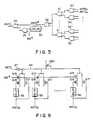
- Fig. 6 shows other constructions of address
transition detecting circuit 20 and pulsewidth extension circuit 21 in the circuit of Fig. 1. Address transition detecting signals φATDL from addresstransition detecting sections 19 are supplied to the gates of N-channel MOS transistors Q17. Address transition detecting signals φATDL are supplied to the gates of N-channel MOS transistors Q18 viarespective delay circuits 36. One-ends of the current paths of MOS transistors Q17 and Q18 are grounded. The other end of the current path of each of MOS transistors Q18 is connected to one end of the current path of a corresponding one of MOS transistors Q19 whose conduction state is controlled by internal write enable signal WE*. The other ends of the current paths of MOS transistors Q17 and the other ends of the current paths of MOS transistors Q19 are connected together. The current path of P-channel MOS transistor Q20 is connected between commonly connected node N4 and the power source. The gate of MOS transistor Q20 is grounded to always keep the MOS transistor in the conductive state. Address transition signals φATD is output frominverter 37 whose input terminal is connected to node N4. - With the above construction, since internal write enable signal WE* is at a low level in the readout mode, each MOS transistor Q19 is set in the nonconductive state, and MOS transistors Q18 and Q19 and delay
circuits 36 have no influence on the operation of the circuit. When address transition detecting signals φATDL are supplied to the gates of respective MOS transistors Q17, at least one of MOS transistors Q17 is turned on, setting the potential of node N4 to a low level. As a result, address transition signal φATD becomes high. When address transition detecting signals φATDL are set to a low level, all the MOS transistors Q17 are turned off, setting the potential of node N4 to a high level. As a result, address transition signal φATD becomes low. - In contrast, since internal write enable signal WE* is at a high level in the write mode, each MOS transistor Q19 is set in the conductive state. When address transition detecting signals φATDL are supplied to the gates of respective MOS transistors Q17, at least one of MOS transistors Q17 is turned on. At this time, address transition signals φATD supplied to the gates of MOS transistors Q18 are delayed by means of
delay circuits 36, and therefore MOS transistors Q18 are still kept nonconductive. MOS transistor Q17 set into the conductive state causes the potential of node N4 to be set to a low level. As a result, address transition signal φATD is set to a high level. When address transition detecting signal φATDL is set to a low level, all the MOS transistors Q17 are turned off. However, since MOS transistor Q18 is turned on with a delay time, node N4 is discharged via MOS transistors Q19 and Q18, thus delaying the rise of the potential of node N4 by a delay time determined bydelay circuit 36. After the delay time caused bydelay circuit 36, MOS transistors Q18 are all turned off and the potential of node N4 rises, causing address transition signal φATD to be set to a low level. - With the construction of Fig. 6, the pulse width of address transition signal φATD is set to be longer in the write mode than in the readout mode in the same manner as in the circuits of Figs. 3 to 5.
Claims (15)
Applications Claiming Priority (2)
| Application Number | Priority Date | Filing Date | Title |
|---|---|---|---|
| JP63076606A JPH0766665B2 (en) | 1988-03-31 | 1988-03-31 | Semiconductor memory device |
| JP76606/88 | 1988-03-31 |
Publications (3)
| Publication Number | Publication Date |
|---|---|
| EP0336319A2 true EP0336319A2 (en) | 1989-10-11 |
| EP0336319A3 EP0336319A3 (en) | 1990-03-07 |
| EP0336319B1 EP0336319B1 (en) | 1993-09-29 |
Family
ID=13609993
Family Applications (1)
| Application Number | Title | Priority Date | Filing Date |
|---|---|---|---|
| EP89105724A Expired - Lifetime EP0336319B1 (en) | 1988-03-31 | 1989-03-31 | Internal synchronization type mos sram with address transition detecting circuit |
Country Status (6)
| Country | Link |
|---|---|
| US (1) | US4916668A (en) |
| EP (1) | EP0336319B1 (en) |
| JP (1) | JPH0766665B2 (en) |
| KR (1) | KR920008031B1 (en) |
| DE (1) | DE68909467T2 (en) |
| MY (1) | MY104082A (en) |
Cited By (6)
| Publication number | Priority date | Publication date | Assignee | Title |
|---|---|---|---|---|
| GB2247759A (en) * | 1990-09-04 | 1992-03-11 | Samsung Electronics Co Ltd | Semiconductor memory address decoder with delayed output. |
| AU642978B2 (en) * | 1991-03-12 | 1993-11-04 | Alcatel N.V. | Method and device for aquisition and alignment of data |
| EP0453678B1 (en) * | 1988-10-28 | 1995-01-11 | STERN & STERN INDUSTRIES, INC. | Low permeability fabric and method of making same |
| EP0794618A1 (en) * | 1996-03-06 | 1997-09-10 | STMicroelectronics S.r.l. | Address transition detection circuit |
| EP0740303A3 (en) * | 1995-04-24 | 1998-12-16 | Nec Corporation | Semiconductor static memory device with pulse generator for reducing write cycle time |
| EP0960421A4 (en) * | 1997-01-24 | 2003-07-09 | Atmel Corp | Bitline load and precharge structure for an sram memory |
Families Citing this family (17)
| Publication number | Priority date | Publication date | Assignee | Title |
|---|---|---|---|---|
| US5228003A (en) * | 1988-04-15 | 1993-07-13 | Seiko Epson Corporation | Semiconductor memory |
| JPH0289286A (en) * | 1988-09-27 | 1990-03-29 | Seiko Epson Corp | semiconductor storage device |
| US5719812A (en) * | 1988-11-16 | 1998-02-17 | Fujitsu Limited | Semiconductor memory including bit line reset circuitry and a pulse generator having output delay time dependent on type of transition in an input signal |
| JPH07118196B2 (en) * | 1988-12-28 | 1995-12-18 | 株式会社東芝 | Static semiconductor memory |
| KR900015148A (en) * | 1989-03-09 | 1990-10-26 | 미다 가쓰시게 | Semiconductor device |
| JP2759689B2 (en) * | 1989-11-24 | 1998-05-28 | 松下電器産業株式会社 | RAM readout circuit |
| US5258952A (en) * | 1990-12-14 | 1993-11-02 | Sgs-Thomson Microelectronics, Inc. | Semiconductor memory with separate time-out control for read and write operations |
| US5243575A (en) * | 1992-06-19 | 1993-09-07 | Intel Corporation | Address transition detection to write state machine interface circuit for flash memory |
| KR0137083B1 (en) * | 1993-09-14 | 1998-04-29 | 세까자와 다다시 | Semiconductor memory device and data reading method |
| JP3778579B2 (en) * | 1993-11-16 | 2006-05-24 | 株式会社ルネサステクノロジ | Semiconductor memory device |
| US5598375A (en) * | 1995-06-23 | 1997-01-28 | Electronics Research & Service Organization | Static random access memory dynamic address decoder with non-overlap word-line enable |
| KR100190366B1 (en) * | 1996-04-10 | 1999-06-01 | 김영환 | Semiconductor memory device and power supply method |
| JPH11126483A (en) * | 1997-10-20 | 1999-05-11 | Fujitsu Ltd | Power saving synchronous circuit and semiconductor memory device having the same |
| US5903502A (en) * | 1997-11-25 | 1999-05-11 | Micron Technology, Inc. | Variable equilibrate voltage circuit for paired digit lines |
| US6252819B1 (en) * | 2000-05-01 | 2001-06-26 | Sandcraft, Inc. | Reduced line select decoder for a memory array |
| US6366493B1 (en) * | 2000-10-24 | 2002-04-02 | United Microelectronics Corp. | Four transistors static-random-access-memory cell |
| JP5262246B2 (en) * | 2008-03-31 | 2013-08-14 | 富士通セミコンダクター株式会社 | Semiconductor memory device and memory system |
Family Cites Families (7)
| Publication number | Priority date | Publication date | Assignee | Title |
|---|---|---|---|---|
| US4592028A (en) * | 1982-06-09 | 1986-05-27 | Tokyo Shibaura Denki Kabushiki Kaisha | Memory device |
| JPS59221891A (en) * | 1983-05-31 | 1984-12-13 | Toshiba Corp | Static semiconductor storage device |
| JPS61104394A (en) * | 1984-10-22 | 1986-05-22 | Mitsubishi Electric Corp | semiconductor storage device |
| JPS61196498A (en) * | 1985-02-26 | 1986-08-30 | Mitsubishi Electric Corp | Semiconductor memory |
| US4636991A (en) * | 1985-08-16 | 1987-01-13 | Motorola, Inc. | Summation of address transition signals |
| JPS6286599A (en) * | 1985-10-09 | 1987-04-21 | Nec Corp | Semiconductor memory device |
| US4811297A (en) * | 1986-12-16 | 1989-03-07 | Fujitsu Limited | Boundary-free semiconductor memory device |
-
1988
- 1988-03-31 JP JP63076606A patent/JPH0766665B2/en not_active Expired - Fee Related
-
1989
- 1989-03-28 MY MYPI89000392A patent/MY104082A/en unknown
- 1989-03-29 US US07/330,048 patent/US4916668A/en not_active Expired - Lifetime
- 1989-03-30 KR KR1019890004081A patent/KR920008031B1/en not_active Expired
- 1989-03-31 EP EP89105724A patent/EP0336319B1/en not_active Expired - Lifetime
- 1989-03-31 DE DE89105724T patent/DE68909467T2/en not_active Expired - Fee Related
Cited By (7)
| Publication number | Priority date | Publication date | Assignee | Title |
|---|---|---|---|---|
| EP0453678B1 (en) * | 1988-10-28 | 1995-01-11 | STERN & STERN INDUSTRIES, INC. | Low permeability fabric and method of making same |
| GB2247759A (en) * | 1990-09-04 | 1992-03-11 | Samsung Electronics Co Ltd | Semiconductor memory address decoder with delayed output. |
| GB2247759B (en) * | 1990-09-04 | 1994-10-12 | Samsung Electronics Co Ltd | Semiconductor memory device |
| AU642978B2 (en) * | 1991-03-12 | 1993-11-04 | Alcatel N.V. | Method and device for aquisition and alignment of data |
| EP0740303A3 (en) * | 1995-04-24 | 1998-12-16 | Nec Corporation | Semiconductor static memory device with pulse generator for reducing write cycle time |
| EP0794618A1 (en) * | 1996-03-06 | 1997-09-10 | STMicroelectronics S.r.l. | Address transition detection circuit |
| EP0960421A4 (en) * | 1997-01-24 | 2003-07-09 | Atmel Corp | Bitline load and precharge structure for an sram memory |
Also Published As
| Publication number | Publication date |
|---|---|
| US4916668A (en) | 1990-04-10 |
| DE68909467D1 (en) | 1993-11-04 |
| JPH0766665B2 (en) | 1995-07-19 |
| EP0336319A3 (en) | 1990-03-07 |
| MY104082A (en) | 1993-11-30 |
| EP0336319B1 (en) | 1993-09-29 |
| KR920008031B1 (en) | 1992-09-21 |
| JPH01251494A (en) | 1989-10-06 |
| DE68909467T2 (en) | 1994-04-07 |
| KR890015272A (en) | 1989-10-28 |
Similar Documents
| Publication | Publication Date | Title |
|---|---|---|
| EP0336319B1 (en) | Internal synchronization type mos sram with address transition detecting circuit | |
| US4417328A (en) | Random access semiconductor memory device using MOS transistors | |
| US5036491A (en) | Multiport semiconductor memory including an address comparator | |
| US4744063A (en) | Static memory utilizing transition detectors to reduce power consumption | |
| US4804871A (en) | Bit-line isolated, CMOS sense amplifier | |
| US5091889A (en) | Semiconductor memory having an operation margin against a write recovery time | |
| US4612631A (en) | Static type semiconductor memory circuit | |
| US5305268A (en) | Semiconductor memory with column equilibrate on change of data during a write cycle | |
| EP0337202B1 (en) | Static random access memory with address transition detector | |
| US5267197A (en) | Read/write memory having an improved write driver | |
| KR100848058B1 (en) | Static memory having self-timing circuit | |
| US4616344A (en) | Static memory circuit | |
| KR970004416B1 (en) | Random-access memory and its read and write circuit as well as read and write method of data packet | |
| JPS631677B2 (en) | ||
| KR100284062B1 (en) | Semiconductor memory circuit | |
| US4558435A (en) | Memory system | |
| JP3606951B2 (en) | Semiconductor memory device | |
| KR950006426B1 (en) | Static memory | |
| EP0547889B1 (en) | A tristatable driver for internal data bus lines | |
| US6356473B1 (en) | Static random access memory (SRAM) | |
| JP3039793B2 (en) | Semiconductor memory device | |
| JPH04298891A (en) | Semiconductor memory having column-decoding type bit-line balance | |
| KR910014938A (en) | Integrated Circuit Memory with Enhanced DI / DT Control | |
| US4739499A (en) | Random access memory using semiconductor data storage elements | |
| EP0199458B1 (en) | Memory circuit having an improved writing scheme |
Legal Events
| Date | Code | Title | Description |
|---|---|---|---|
| PUAI | Public reference made under article 153(3) epc to a published international application that has entered the european phase |
Free format text: ORIGINAL CODE: 0009012 |
|
| 17P | Request for examination filed |
Effective date: 19890331 |
|
| AK | Designated contracting states |
Kind code of ref document: A2 Designated state(s): DE FR GB |
|
| PUAL | Search report despatched |
Free format text: ORIGINAL CODE: 0009013 |
|
| AK | Designated contracting states |
Kind code of ref document: A3 Designated state(s): DE FR GB |
|
| 17Q | First examination report despatched |
Effective date: 19921204 |
|
| GRAA | (expected) grant |
Free format text: ORIGINAL CODE: 0009210 |
|
| AK | Designated contracting states |
Kind code of ref document: B1 Designated state(s): DE FR GB |
|
| REF | Corresponds to: |
Ref document number: 68909467 Country of ref document: DE Date of ref document: 19931104 |
|
| ET | Fr: translation filed | ||
| PLBE | No opposition filed within time limit |
Free format text: ORIGINAL CODE: 0009261 |
|
| STAA | Information on the status of an ep patent application or granted ep patent |
Free format text: STATUS: NO OPPOSITION FILED WITHIN TIME LIMIT |
|
| 26N | No opposition filed | ||
| PGFP | Annual fee paid to national office [announced via postgrant information from national office to epo] |
Ref country code: GB Payment date: 19970324 Year of fee payment: 9 |
|
| PGFP | Annual fee paid to national office [announced via postgrant information from national office to epo] |
Ref country code: FR Payment date: 19980310 Year of fee payment: 10 |
|
| PG25 | Lapsed in a contracting state [announced via postgrant information from national office to epo] |
Ref country code: GB Free format text: LAPSE BECAUSE OF NON-PAYMENT OF DUE FEES Effective date: 19980331 |
|
| GBPC | Gb: european patent ceased through non-payment of renewal fee |
Effective date: 19980331 |
|
| PG25 | Lapsed in a contracting state [announced via postgrant information from national office to epo] |
Ref country code: FR Free format text: LAPSE BECAUSE OF NON-PAYMENT OF DUE FEES Effective date: 19991130 |
|
| REG | Reference to a national code |
Ref country code: FR Ref legal event code: ST |
|
| PGFP | Annual fee paid to national office [announced via postgrant information from national office to epo] |
Ref country code: DE Payment date: 20060323 Year of fee payment: 18 |
|
| PG25 | Lapsed in a contracting state [announced via postgrant information from national office to epo] |
Ref country code: DE Free format text: LAPSE BECAUSE OF NON-PAYMENT OF DUE FEES Effective date: 20071002 |