EP0330105B1 - Integrierte Dünnschichtmembrane - Google Patents
Integrierte Dünnschichtmembrane Download PDFInfo
- Publication number
- EP0330105B1 EP0330105B1 EP89102852A EP89102852A EP0330105B1 EP 0330105 B1 EP0330105 B1 EP 0330105B1 EP 89102852 A EP89102852 A EP 89102852A EP 89102852 A EP89102852 A EP 89102852A EP 0330105 B1 EP0330105 B1 EP 0330105B1
- Authority
- EP
- European Patent Office
- Prior art keywords
- etch
- silicon
- sacrificial
- process according
- thin film
- Prior art date
- Legal status (The legal status is an assumption and is not a legal conclusion. Google has not performed a legal analysis and makes no representation as to the accuracy of the status listed.)
- Expired - Lifetime
Links
Images
Classifications
-
- H—ELECTRICITY
- H10—SEMICONDUCTOR DEVICES; ELECTRIC SOLID-STATE DEVICES NOT OTHERWISE PROVIDED FOR
- H10P—GENERIC PROCESSES OR APPARATUS FOR THE MANUFACTURE OR TREATMENT OF DEVICES COVERED BY CLASS H10
- H10P50/00—Etching of wafers, substrates or parts of devices
- H10P50/60—Wet etching
- H10P50/64—Wet etching of semiconductor materials
- H10P50/642—Chemical etching
- H10P50/644—Anisotropic liquid etching
-
- G—PHYSICS
- G01—MEASURING; TESTING
- G01F—MEASURING VOLUME, VOLUME FLOW, MASS FLOW OR LIQUID LEVEL; METERING BY VOLUME
- G01F1/00—Measuring the volume flow or mass flow of fluid or fluent solid material wherein the fluid passes through a meter in a continuous flow
- G01F1/68—Measuring the volume flow or mass flow of fluid or fluent solid material wherein the fluid passes through a meter in a continuous flow by using thermal effects
- G01F1/684—Structural arrangements; Mounting of elements, e.g. in relation to fluid flow
- G01F1/6845—Micromachined devices
-
- Y—GENERAL TAGGING OF NEW TECHNOLOGICAL DEVELOPMENTS; GENERAL TAGGING OF CROSS-SECTIONAL TECHNOLOGIES SPANNING OVER SEVERAL SECTIONS OF THE IPC; TECHNICAL SUBJECTS COVERED BY FORMER USPC CROSS-REFERENCE ART COLLECTIONS [XRACs] AND DIGESTS
- Y10—TECHNICAL SUBJECTS COVERED BY FORMER USPC
- Y10T—TECHNICAL SUBJECTS COVERED BY FORMER US CLASSIFICATION
- Y10T29/00—Metal working
- Y10T29/49—Method of mechanical manufacture
- Y10T29/49002—Electrical device making
- Y10T29/49082—Resistor making
- Y10T29/49103—Strain gauge making
Definitions
- the invention is directed to the field of microsensor mass air flow devices and a method of fabricating the devices.
- the structure at an intermediate point of fabrication is a single crystal silicon substrate chip having on a portion of the surface a thin sacrificial layer of nickel-iron, titanium-tungsten, chrome, aluminium or other selectively etchable layer which delineates the future location of a web or diaphragm to be formed at a later step.
- the sacrificial layer and the rest of the silicon chip surface are coated with a thin film of silicon nitride which forms the diaphragm.
- sacrificial layer is meant a layer which is removed at a later stage in the fabrication process.
- a "Monolithic Pressure-Flow Sensor” comprising two membranes, the first of which is made of single crystal silicon and has four diffused piezoresistors on the edge of its surface for pressure-sensing.
- the second membrane made of oxidized porous silicon has a rectangular meander platinium thin film resistor on the center of its surface which is used as a heating element.
- the rim of the chip has also a rectangular meander platinium thin film resistor that is used as a fluid temperature-sensing element.
- the starting material for manufacturing this sensor is a p-type (100) oriented silicon wafer, and the process begins with an initial oxidation and patterning on the front and back sides of the wafer.
- a lightly doped n-type layer is then formed by phosphor ion implantation followed by oxidation and annealing. After annealing a pattern defining the p-type areas in the n-type layer on the front side of the wafer is formed.
- the pattern on the back side of the wafer is also formed in order to obtain uniform anodic current distribution.
- boron diffusion is performed.
- the porous silicon is formed selectively by anodic reaction in 50 percent hydrofluoric acid.
- the n-type layer is not changed to porous silicon.
- the p-type resistors are also not changed to porous silicon because they are electrically isolated from the n-type layer by p-n junction.
- a film of silicon nitride is formed by low pressure chemical-vapor deposition.
- a layer of titanium-platinium is evaporated and patterned using liftoff The titanium serves as an adhesion layer.
- contact holes in the front side of the wafer and windows on the back side of the wafer are formed in the silicon nitride using reactive ion etching.
- Aluminium is then deposited and patterned by wet chemical etching.
- a silicon nitride film is deposited by plasma chemical-vapor deposition and contact cutouts are made over the contact pad areas.
- the membranes are formed by etching the exposed silicon on the back side of the wafer in an anisotropic etching solution containing potassium hydroxide and water.
- the pit or cavity in the silicon beneath the diaphragm is formed by backside etching.
- a precisely defined web or diaphragm area can be fabricated by backside etching without regard to dimensional variations of the backside etch pattern or tolerance variations in the thickness of the silicon wafer and without the necessity of accurate alignment of backside features with front side features. It is not necessary to dope the silicon to achieve the desired precision of position and area of the web. Preferred details and embodiments of the invention are described in the dependent claims.
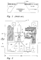
- FIG. 10 there is shown generally at 10 the top plan view of the thin film microsensor chip for air flow sensing constructed on a (100) monocrystalline silicon chip or wafer substrate 11.
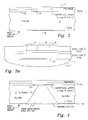
- FIGs 3 and 3a there is shown several of the thin film layers which are not apparent in Figure 2.
- Figure 3 is the structure at an intermediate step in the fabrication prior to removal of the sacrificial layer and etching of a pit in the silicon.
- the monocrystalline silicon substrate wafer 11 has a (100) planar surface 12 which has first formed thereon a thin sacrificial selectively etchable layer such as of sputter deposited Ti:W, Cr, or NiFe 13 preferably about 500-1000 angstroms in thickness.
- the layer 13 is a square about 325 microns ( ⁇ ) on a side.
- the sacrificial layer 13 defines the location of an area where a pit will later be etched in the silicon.
- the critical edges of the sacrificial layer delineation are oriented orthogonally to the ⁇ 110 ⁇ direction to accurately define the final etch pit boundaries. If a non- orthogonal orientation were used, the sacrificial layer delineation itself would not then limit the boundaries of the etch pit.
- a thin film layer of dielectric 14 such as silicon nitride which may be on the order of 2500 to 7000 angstroms ( ⁇ ) thick.
- a thin film electrically resistive layer such as platinum 15 is sputter deposited over the silicon nitride layer 14 and is delineated by conventional techniques into the desired circuit pattern for the chap.
- the platinum film is preferably on the order of 800 angstroms in thickness. No sloped edge is needed to carry the resistor line over the nitride step because the initial sacrificial layer step is small and can easily be covered with nitride, and the metal resistor line can be deposited over the resulting 500 ⁇ vertical nitride step to achieve electrical continuity and chemical passivation.
- a further thin film layer 16 of sputter deposited silicon nitride covers the resistive circuit and the layer 14.
- An optional layer of polyimide 17 may be deposited over layer 16.
- a thin layer of silicon nitride 18 also covers the backside of the wafer.
- a resistive temperature sensor 20 extends between pad A and pad G; a resistor R A extends between pad F and pad D; and a resistor R B extends between pad C and pad D.
- the resistor R B is in the form of a conventional ladder trip network. All of these resistive element including 20, R A and R B as well as a heater and detector (shown as 21) to be described later, are formed in the platinum layer 15, previously identified.
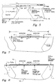
- the heater and detector 21 are formed in a thin web or diaphragm area 22 over an etched pit in the silicon which is shown in more detail in Figures 4, 5 and 7.
- Figure 6 there is shown a more detailed top plan view of the nitride web area 22 which in one preferred embodiment is about 325 microns on a side.
- Figure 6 shows a heater 24 with its leads 25 and 26, an upstream detector area 30 with its leads 31 and 32, a downstream detector area 33 with its leads 34 and 35.
- Figure 7 is a cross-section of the silicon nitride web area 22 shown in Figure 6.
- the heater 24 and detectors 30 and 33 and thin encapsulating silicon nitride film 70 (same as 14,16) on the web area are deposited by conventional thin film techniques as described in earlier patents assigned to the same assignee as the present invention, such as 4,478,076; 4,478,077; 4,501,144; 4,581,928; and 4,651,564.
- a heated element air flow sensor must retain a constant thermal conductance structure over its life to maintain its initial calibration.
- the accumulation of contaminating films or dirt underneath the web structure during life can change the conductance to the silicon and cause error in the calibration.
- An object of the invention is to effectively seal off the pit space beneath the heater and detectors (i.e., the web) from the airflow to prevent such contamination by using a novel back surface etching procedure.
- the backside etching method proceeds substantially as follows.
- the device of Figure 3 first has a nitride cut 19 made on the backside of the wafer to expose an area of the silicon 11 (see Figure 4).
- the preferred pattern of the nitride cut is rectangular or square and is orthogonal to the ⁇ 110 ⁇ direction.
- An anisotropic KOH alkaline etchant is applied to the backside to anisotropically etch a first etch pit 19′ into the silicon until the sacrificial layer is reached.
- the sacrificial layer 13, such as of Ni-Fe, Cr, Ti:W or the like acts as an etch stop for the anisotropic etch used to define the backside cavity.
- the first anisotropic etched pit is formed with its truncated apex somewhere near the middle of the web area as shown in Figure 4.
- the etching action stops when the sacrificial layer is reached, and is limited on the sides by the highly resistant (111) planes of the silicon.
- the sacrificial layer is used to accurately define the area of the diaphragm or web.
- the pattern of the sacrificial layer is square or rectangular with the sides oriented orthogonal to the ⁇ 110 ⁇ direction in the silicon.
- the edge of the pit and hence the length of the bridge are determined by the (111) plane stopping action.
- This is made possible by the orthogonal orientation or the rectangularly delineated sacrificial film beneath the orthogonally oriented microbridge structure, as in Figure 6.
- a second etch is applied into the first etch it to remove the sacrificial layer.
- the sacrificial film is completely removed by a selective etchant thus undercutting the microbridge with a thin 500 angstrom space 27 formerly occupied by the sacrificial layer 13.
- Ni-Fe, Ti:W and Cr materials are: For Ni-Fe 30 parts sulfuric acid 9 parts water 1 part conc. hydrogen peroxide Room temperature For Ti:W 10 parts water 1 part conc. hydrogen peroxide 60 degrees C For Cr 181 grams/liter Cerric ammonium nitride 48 ml/liter acetic acid Water to make 1 liter of solution Room temperature The silicon anisotropic etch is again applied and can fill the newly formed space 27.
- the etching process proceeds slightly differently when the anisotropic KOH etchant reaches the sacrificial layer.
- the sacrificial layer acted as an etch stop.
- the aluminum sacrificial layer is one which is also etched by the KOH etch. This aluminum material is isotropically etched by the KOH at a much higher rate than the KOH etches silicon. Depending on the thickness of the Si wafer, 4-6 hours would be required to etch through the back of the wafer in order to make contact with the sacrificial layer. The etch out of the Al would then proceed very rapidly.
- a variation of the second embodiment may be desirable when platinum is used for the heater 24, the detectors 30 and 33 and the like.
- a diffusion barrier is sometimes needed to prevent aluminum or other sacrificial layer metal from reacting with the Si and thereby prevent or inhibit the anisotropic etching of Si.
- Aluminum (in contact with Si) will form the silicide at 570 degrees C. Since Pt must be annealed at temperatures in excess of this (600-700 degrees C), aluminum silicide will be formed during the stabilization anneal sequence. The silicide can be difficult to remove and can interfere with the anisotropic Si etch process.
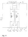
- a diffusion barrier 71 such as SiO2, can be utilized to prevent silicide formation (see Figure 8).
- SiO2 500A-1000A (and even less) of SiO2 is effective in isolating the Al from Si.
- SiO2 can be removed with a standard buffered HF etchant (10:1 BOE).
- the etch rate of SiO2 in BOE is 500-600A/minute.
- SiO2 also etches in the standard anisotropic etch solution at 70A/minute. When the backside etch reaches the diffusion barrier, the SiO2 will be removed (or substantially removed in 10-15 minutes (with a SiO2 thickness of 500A).
- the SiO2 etch-out should be allowed to proceed to (essentially) completion.
- the sacrificial layer can then be removed with the proper etchant.
- the backside etching process will automatically proceed through the various steps - culminating in the final step to etch (downward) from the bottom of the diaphragm, to form the "hour glass" pit structure.
Landscapes
- Physics & Mathematics (AREA)
- Fluid Mechanics (AREA)
- General Physics & Mathematics (AREA)
- Pressure Sensors (AREA)
- Weting (AREA)
Claims (10)
- Verfahren zur Herstellung eines Dünnschicht-Mikrosensors für Luftströmung, gekennzeichnet durch die Schritte:a) Bereitstellen einer (100) Einkristall-Siliziumscheibe (11) mit einer ebenen (100) Vorderfläche sowie einer ebenen (100) Rückfläche;b) Niederschlagen und Anreißen einer rechtwinkligen Fläche (13) einer Dünnschicht aus entfernbarem selektiv ätzbaren Material auf der Siliziumvorderfläche (12) derart, daß zwei sich gegenüberliegende Seiten der rechtwinkligen Fläche sich rechtwinklig zur 〈110〉 Richtung des Kristalls erstrecken;c) Abscheiden einer Dünnschicht (14) aus Siliziumnitrid auf dem selektiv ätzbaren Material (13) und der restlichen Siliziumvorderfläche (12), wobei die Schicht dicker ist als die Dicke des entfernbaren Materials;d) Abscheiden und Anreißen einer Dünnschicht (15) aus elektrischem Widerstandsmaterial auf dem Siliziumnitrid (14), um die gewünschten Schaltkreiselemente wie Detektorwiderstände, Schaltkreiswiderstände und einen Heizwiderstand zu bilden, wobei der Heizwiderstand und die Detektorwiderstände sich oberhalb der Fläche (13) aus entfernbarem Material befinden;e) Niederschlagen einer zusätzlichen Dünnschicht (16) aus Siliziumnitrid auf dem Widerstandsmaterial (15) und dem vorangehenden Siliziumnitrid (14);f) Abscheiden einer Dünnschicht (18) aus Siliziumnitrid auf der rückseitigen Oberfläche;g) Einschneiden einer Öffnung (19) durch das Siliziumnitrid (18) auf der Rückseite, um eine Fläche der rückseitigen Siliziumoberfläche freizulegen, wobei die Öffnung rechtwinklig ist und zwei sich gegenüberliegende Kanten sich rechtwinklig zur 〈110〉 Richtung erstrecken;h) Aufbringen eines anisotropen Ätzmittels auf die rückseitige Siliziumoberfläche im Bereich der Öffnung im Nitrid zwecks anisotroper Ätzung einer ersten anisotropen Mulde (19') durch die Siliziumscheibe (11) bis zum Erreichen der Schicht (13) aus entfernbarem selektiv ätzbaren Material;i) Einfüllen eines selektiven Ätzmittels durch die erste anisotrope Mulde zwecks Ausätzung allen entfernbaren selektiv ätzbaren Materials (13) und Erzeugung eines dünnen Hohlraums (27) anstelle des weggeätzten Materials; undj) Einführen des anisotropen Ätzmittels durch die erste Mulde und dünnen Hohlraum zum anisotropen Ätzen des Siliziums (28), welches durch das Entfernen des entfernbaren Materials (13) freigelegt wurde, und Bilden einer zweiten anisotropen Ätzmulde (29).
- Verfahren nach Anspruch 1, dadurch gekennzeichnet, daß das entfernbare selektiv ätzbare Material (13) aus einer Gruppe ausgewählt ist, welche aus NiFe, Cr und Ti:W besteht und wobei das selektiv ätzbare Material als Ätzsperre für das anisotrope Ätzmittel dient.
- Verfahren nach Anspruch 1 oder 2, dadurch gekennzeichnet, daß die Dünnschicht (13) aus entfernbarem selektiv ätzbaren Material etwa 500 bis 1000Å dick ist.
- Verfahren nach Anspruch 1, 2 oder 3, bei dem das entfernbare Material NiFe ist, dadurch gekennzeichnet, daß das selektive Ätzmittel aus 30 Teilen schwefliger Säure, 9 Teilen Wasser und einem Teil konzentriertem Wasserstoffperoxyd bei Raumtemperatur besteht.
- Verfahren nach Anspruch 1, 2 oder 3, bei dem das entfernbare Material Ti:W ist, dadurch gekennzeichnet, daß das selektive Ätzmittel für Ti:W aus 10 Teilen Wasser und einem Teil konzentriertem Wasserstoffperoxyd bei 60°C besteht.
- Verfahren nach Anspruch 1, 2 oder 3, bei dem das entfernbare Material Cr ist, dadurch gekennzeichnet, daß das selektive Ätzmittel für Cr aus 181 Gramm/Liter Zer-Ammoniumnitrid, 48 m/Liter Essigsäure sowie Wasser besteht, so daß ein Liter Lösung bei Raumtemperatur entsteht.
- Verfahren nach einem der vorangehenden Ansprüche, dadurch gekennzeichnet, daß das anisotrope Ätzmittel KOH ist.
- Verfahren nach einem der vorangehenden Ansprüche, dadurch gekennzeichnet, daß das entfernbare selektiv ätzbare Material (13) Aluminium ist.
- Verfahren nach Anspruch 7 und 8, bei dem das anisotrope Ätzmittel auch ein selektives Ätzmittel für Aluminium ist und wobei die drei Ätzschritte ein fortlaufendes Verfahren sind.
- Verfahren nach einem der vorangehenden Ansprüche, gekennzeichnet durch den weiteren Schritt der Bildung einer Sauerstoffdiffusionssperre (71) von etwa 500 bis 1000Å SiO₂ auf der ebenen Vorderfläche (12) der Siliziumscheibe (10) vor dem Niederschlagen und Anreißen des entfernbaren selektiv ätzbaren Materials (13).
Applications Claiming Priority (2)
| Application Number | Priority Date | Filing Date | Title |
|---|---|---|---|
| US158824 | 1988-02-22 | ||
| US07/158,824 US4784721A (en) | 1988-02-22 | 1988-02-22 | Integrated thin-film diaphragm; backside etch |
Publications (3)
| Publication Number | Publication Date |
|---|---|
| EP0330105A2 EP0330105A2 (de) | 1989-08-30 |
| EP0330105A3 EP0330105A3 (de) | 1991-11-13 |
| EP0330105B1 true EP0330105B1 (de) | 1994-12-14 |
Family
ID=22569872
Family Applications (1)
| Application Number | Title | Priority Date | Filing Date |
|---|---|---|---|
| EP89102852A Expired - Lifetime EP0330105B1 (de) | 1988-02-22 | 1989-02-18 | Integrierte Dünnschichtmembrane |
Country Status (5)
| Country | Link |
|---|---|
| US (1) | US4784721A (de) |
| EP (1) | EP0330105B1 (de) |
| JP (1) | JPH01309384A (de) |
| CA (1) | CA1295055C (de) |
| DE (1) | DE68919870T2 (de) |
Cited By (2)
| Publication number | Priority date | Publication date | Assignee | Title |
|---|---|---|---|---|
| DE10161047B4 (de) * | 2000-12-13 | 2011-06-01 | Denso Corporation, Kariya-City | Verfahren zur Herstellung eines Sensors mit Membranstruktur |
| TWI447365B (zh) * | 2011-05-24 | 2014-08-01 | Univ Nat Kaohsiung Applied Sci | Single crystal silicon thermal sensor and its preparation method |
Families Citing this family (108)
| Publication number | Priority date | Publication date | Assignee | Title |
|---|---|---|---|---|
| US4975390A (en) * | 1986-12-18 | 1990-12-04 | Nippondenso Co. Ltd. | Method of fabricating a semiconductor pressure sensor |
| GB2215914B (en) * | 1988-03-17 | 1991-07-03 | Emi Plc Thorn | A microengineered diaphragm pressure switch and a method of manufacture thereof |
| US5354695A (en) | 1992-04-08 | 1994-10-11 | Leedy Glenn J | Membrane dielectric isolation IC fabrication |
| US4996627A (en) * | 1989-01-30 | 1991-02-26 | Dresser Industries, Inc. | High sensitivity miniature pressure transducer |
| US4889590A (en) * | 1989-04-27 | 1989-12-26 | Motorola Inc. | Semiconductor pressure sensor means and method |
| US4930347A (en) * | 1989-05-23 | 1990-06-05 | University Of Cincinnati | Solid state microanemometer with improved sensitivity and response time |
| US5115291A (en) * | 1989-07-27 | 1992-05-19 | Honeywell Inc. | Electrostatic silicon accelerometer |
| DE4003472C2 (de) * | 1989-09-22 | 1999-08-12 | Bosch Gmbh Robert | Verfahren zum anisotropen Ätzen von Siliziumplatten |
| GB8921722D0 (en) * | 1989-09-26 | 1989-11-08 | British Telecomm | Micromechanical switch |
| US5030318A (en) * | 1989-09-28 | 1991-07-09 | Polycon Corporation | Method of making electrical probe diaphragms |
| US4961821A (en) * | 1989-11-22 | 1990-10-09 | Xerox Corporation | Ode through holes and butt edges without edge dicing |
| US5163329A (en) * | 1989-12-29 | 1992-11-17 | Kabushiki Kaisha Toyota Chuo Kenkyusho | Semiconductor pressure sensor |
| DE69112251T2 (de) * | 1990-04-13 | 1996-02-22 | Yamatake Honeywell Co Ltd | Membransensor. |
| DE4012080A1 (de) * | 1990-04-14 | 1991-10-17 | Bosch Gmbh Robert | Verfahren zum aufbau von mikromechanischen sensoren |
| DE4012071A1 (de) * | 1990-04-14 | 1991-10-17 | Bosch Gmbh Robert | Verfahren zur herstellung mikromechanischer strukturen |
| US5056362A (en) * | 1990-07-25 | 1991-10-15 | Siemens Automotive L.P. | Strengthening a silicon micromachined mass air flow sensor in the region of its hot element |
| JP2558549B2 (ja) * | 1990-10-11 | 1996-11-27 | 東横化学株式会社 | 半導体圧力センサ及びその製造方法 |
| US5231877A (en) * | 1990-12-12 | 1993-08-03 | University Of Cincinnati | Solid state microanemometer |
| US5220838A (en) * | 1991-03-28 | 1993-06-22 | The Foxboro Company | Overpressure-protected, differential pressure sensor and method of making the same |
| JP2992848B2 (ja) * | 1991-08-21 | 1999-12-20 | 株式会社山武 | 熱伝導率検出器 |
| US6714625B1 (en) * | 1992-04-08 | 2004-03-30 | Elm Technology Corporation | Lithography device for semiconductor circuit pattern generation |
| US5985693A (en) * | 1994-09-30 | 1999-11-16 | Elm Technology Corporation | High density three-dimensional IC interconnection |
| US5323656A (en) * | 1992-05-12 | 1994-06-28 | The Foxboro Company | Overpressure-protected, polysilicon, capacitive differential pressure sensor and method of making the same |
| DE4215722C2 (de) * | 1992-05-13 | 1997-02-13 | Bosch Gmbh Robert | Sensorsubstrat mit einer Membran und Verfahren zu deren Herstellung |
| EP0660967B1 (de) * | 1992-09-14 | 2001-04-11 | Shellcase Ltd. | Verfahren zum herstellen integrierte schaltungsanordnungen |
| DE4233153C2 (de) * | 1992-10-02 | 1995-08-17 | Lang Apparatebau Gmbh | Kalorimetrischer Durchflußmesser und Verfahren zu seiner Herstellung |
| US5464966A (en) * | 1992-10-26 | 1995-11-07 | The United States Of America As Represented By The Secretary Of Commerce | Micro-hotplate devices and methods for their fabrication |
| US5332469A (en) * | 1992-11-12 | 1994-07-26 | Ford Motor Company | Capacitive surface micromachined differential pressure sensor |
| DE4338890A1 (de) * | 1993-02-25 | 1994-09-01 | Bosch Gmbh Robert | Massenflußsensor |
| US5356513A (en) * | 1993-04-22 | 1994-10-18 | International Business Machines Corporation | Polishstop planarization method and structure |
| US5413679A (en) * | 1993-06-30 | 1995-05-09 | The United States Of America As Represented By The Secretary Of The Navy | Method of producing a silicon membrane using a silicon alloy etch stop layer |
| US5461922A (en) * | 1993-07-27 | 1995-10-31 | Lucas-Novasensor | Pressure sensor isolated within housing having integral diaphragm and method of making same |
| AT404758B (de) * | 1993-07-29 | 1999-02-25 | Urban Gerald Dipl Ing Dr | Miniatur-sonde, verfahren zu ihrer herstellung und deren verwendung |
| IL106892A0 (en) * | 1993-09-02 | 1993-12-28 | Pierre Badehi | Methods and apparatus for producing integrated circuit devices |
| JP3333948B2 (ja) * | 1994-02-23 | 2002-10-15 | 本田技研工業株式会社 | ガス式センサの製造方法 |
| US5533393A (en) * | 1995-01-13 | 1996-07-09 | Honeywell Inc. | Determination of dew point or absolute humidity |
| US5736430A (en) * | 1995-06-07 | 1998-04-07 | Ssi Technologies, Inc. | Transducer having a silicon diaphragm and method for forming same |
| CA2176052A1 (en) * | 1995-06-07 | 1996-12-08 | James D. Seefeldt | Transducer having a resonating silicon beam and method for forming same |
| US6021675A (en) * | 1995-06-07 | 2000-02-08 | Ssi Technologies, Inc. | Resonating structure and method for forming the resonating structure |
| US5804462A (en) * | 1995-11-30 | 1998-09-08 | Motorola, Inc. | Method for forming a multiple-sensor semiconductor chip |
| US5888845A (en) * | 1996-05-02 | 1999-03-30 | National Semiconductor Corporation | Method of making high sensitivity micro-machined pressure sensors and acoustic transducers |
| US5891354A (en) * | 1996-07-26 | 1999-04-06 | Fujitsu Limited | Methods of etching through wafers and substrates with a composite etch stop layer |
| US6547973B2 (en) | 1996-07-30 | 2003-04-15 | Agilent Technologies, Inc. | Fabrication of suspended structures using a sacrificial layer |
| CN1077283C (zh) * | 1996-08-23 | 2002-01-02 | 李韫言 | 一种微细加工的热式流量传感器及其制造方法 |
| DE19643763A1 (de) * | 1996-10-23 | 1998-05-07 | Itt Ind Gmbh Deutsche | Verfahren zum Bearbeiten eines Gebietes in einem Halbleiterwafer |
| JP3984689B2 (ja) * | 1996-11-11 | 2007-10-03 | キヤノン株式会社 | インクジェットヘッドの製造方法 |
| DE69730667T2 (de) * | 1996-11-11 | 2005-09-22 | Canon K.K. | Verfahren zur Herstellung eines Durchgangslochs, Gebrauch dieses Verfahrens zur Herstellung eines Slikonsubstrates mit einem solchen Durchgangsloch oder eine Vorrichtung mit diesem Substrat, Verfahren zur Herstellung eines Tintenstrahl-Druckkopfes und Gebrauch dieses Verfahrens zur Herstellung eines Tintenstrahldruckkopfes |
| DE19711874C2 (de) * | 1997-03-21 | 1999-08-12 | Max Planck Gesellschaft | Folienmanometer |
| US5915167A (en) | 1997-04-04 | 1999-06-22 | Elm Technology Corporation | Three dimensional structure memory |
| US6551857B2 (en) | 1997-04-04 | 2003-04-22 | Elm Technology Corporation | Three dimensional structure integrated circuits |
| US6514875B1 (en) | 1997-04-28 | 2003-02-04 | The Regents Of The University Of California | Chemical method for producing smooth surfaces on silicon wafers |
| US7465030B2 (en) | 1997-07-15 | 2008-12-16 | Silverbrook Research Pty Ltd | Nozzle arrangement with a magnetic field generator |
| US7337532B2 (en) | 1997-07-15 | 2008-03-04 | Silverbrook Research Pty Ltd | Method of manufacturing micro-electromechanical device having motion-transmitting structure |
| US6712453B2 (en) | 1997-07-15 | 2004-03-30 | Silverbrook Research Pty Ltd. | Ink jet nozzle rim |
| AUPP398798A0 (en) * | 1998-06-09 | 1998-07-02 | Silverbrook Research Pty Ltd | Image creation method and apparatus (ij43) |
| US7468139B2 (en) | 1997-07-15 | 2008-12-23 | Silverbrook Research Pty Ltd | Method of depositing heater material over a photoresist scaffold |
| US6855264B1 (en) | 1997-07-15 | 2005-02-15 | Kia Silverbrook | Method of manufacture of an ink jet printer having a thermal actuator comprising an external coil spring |
| US7195339B2 (en) | 1997-07-15 | 2007-03-27 | Silverbrook Research Pty Ltd | Ink jet nozzle assembly with a thermal bend actuator |
| US7556356B1 (en) | 1997-07-15 | 2009-07-07 | Silverbrook Research Pty Ltd | Inkjet printhead integrated circuit with ink spread prevention |
| US6935724B2 (en) | 1997-07-15 | 2005-08-30 | Silverbrook Research Pty Ltd | Ink jet nozzle having actuator with anchor positioned between nozzle chamber and actuator connection point |
| US6682174B2 (en) | 1998-03-25 | 2004-01-27 | Silverbrook Research Pty Ltd | Ink jet nozzle arrangement configuration |
| US6648453B2 (en) | 1997-07-15 | 2003-11-18 | Silverbrook Research Pty Ltd | Ink jet printhead chip with predetermined micro-electromechanical systems height |
| DE19752208A1 (de) * | 1997-11-25 | 1999-06-02 | Bosch Gmbh Robert | Thermischer Membransensor und Verfahren zu seiner Herstellung |
| US6076409A (en) * | 1997-12-22 | 2000-06-20 | Rosemount Aerospace, Inc. | Media compatible packages for pressure sensing devices |
| US6311561B1 (en) | 1997-12-22 | 2001-11-06 | Rosemount Aerospace Inc. | Media compatible pressure sensor |
| US6156585A (en) * | 1998-02-02 | 2000-12-05 | Motorola, Inc. | Semiconductor component and method of manufacture |
| US6261870B1 (en) * | 1998-08-28 | 2001-07-17 | Lsi Logic Corporation | Backside failure analysis capable integrated circuit packaging |
| AU5901100A (en) * | 1999-06-29 | 2001-01-31 | Regents Of The University Of Minnesota | Micro-electromechanical devices and methods of manufacture |
| US6816301B1 (en) | 1999-06-29 | 2004-11-09 | Regents Of The University Of Minnesota | Micro-electromechanical devices and methods of manufacture |
| EP1092962A3 (de) * | 1999-09-30 | 2002-01-23 | Sensirion AG | Offset-Reduktion an Massenflusssensor |
| US6647796B2 (en) * | 2000-08-11 | 2003-11-18 | California Institue Of Technology | Semiconductor nitride pressure microsensor and method of making and using the same |
| US6622558B2 (en) | 2000-11-30 | 2003-09-23 | Orbital Research Inc. | Method and sensor for detecting strain using shape memory alloys |
| US6631638B2 (en) | 2001-01-30 | 2003-10-14 | Rosemount Aerospace Inc. | Fluid flow sensor |
| US20030021572A1 (en) * | 2001-02-07 | 2003-01-30 | Steinberg Dan A. | V-groove with tapered depth and method for making |
| US6907150B2 (en) * | 2001-02-07 | 2005-06-14 | Shipley Company, L.L.C. | Etching process for micromachining crystalline materials and devices fabricated thereby |
| US6885786B2 (en) | 2001-02-07 | 2005-04-26 | Shipley Company, L.L.C. | Combined wet and dry etching process for micromachining of crystalline materials |
| US6964804B2 (en) * | 2001-02-14 | 2005-11-15 | Shipley Company, L.L.C. | Micromachined structures made by combined wet and dry etching |
| US6896850B2 (en) * | 2001-03-26 | 2005-05-24 | Kumetrix, Inc. | Silicon nitride window for microsampling device and method of construction |
| US6748994B2 (en) | 2001-04-11 | 2004-06-15 | Avery Dennison Corporation | Label applicator, method and label therefor |
| US20020195417A1 (en) * | 2001-04-20 | 2002-12-26 | Steinberg Dan A. | Wet and dry etching process on <110> silicon and resulting structures |
| DE10129346B4 (de) * | 2001-06-19 | 2006-08-31 | Infineon Technologies Ag | Verfahren zur Herstellung eines Halbleiterbauelementes |
| JP4590791B2 (ja) * | 2001-07-03 | 2010-12-01 | 株式会社デンソー | センサの製造方法 |
| EP1414609A4 (de) * | 2001-07-19 | 2012-03-28 | Samsung Electronics Co Ltd | Ätzprozess zur mikrobearbeitung von kristallinen materialien und dadurch hergestellte vorrichtungen |
| US7003125B2 (en) * | 2001-09-12 | 2006-02-21 | Seung-Hwan Yi | Micromachined piezoelectric microspeaker and fabricating method thereof |
| US7402897B2 (en) | 2002-08-08 | 2008-07-22 | Elm Technology Corporation | Vertical system integration |
| JP2004206998A (ja) * | 2002-12-25 | 2004-07-22 | Nissan Motor Co Ltd | 固体酸化物形燃料電池用セル、セル板及びその製造方法 |
| JP2004228273A (ja) * | 2003-01-22 | 2004-08-12 | Renesas Technology Corp | 半導体装置 |
| TWI254025B (en) | 2003-05-23 | 2006-05-01 | Rohm & Haas Elect Mat | Etching process for micromachining crystalline materials and devices fabricated thereby |
| US6859330B2 (en) * | 2003-06-04 | 2005-02-22 | Intel Corporation | Micromachined pellicle splitters and tunable laser modules incorporating same |
| US7455787B2 (en) * | 2003-08-01 | 2008-11-25 | Sunpower Corporation | Etching of solar cell materials |
| US7211873B2 (en) * | 2003-09-24 | 2007-05-01 | Denso Corporation | Sensor device having thin membrane and method of manufacturing the same |
| US7368313B2 (en) * | 2004-02-17 | 2008-05-06 | Robert Bosch Gmbh | Method of making a differential pressure sensor |
| US8088293B2 (en) | 2004-07-29 | 2012-01-03 | Micron Technology, Inc. | Methods of forming reticles configured for imprint lithography |
| US7276453B2 (en) * | 2004-08-10 | 2007-10-02 | E.I. Du Pont De Nemours And Company | Methods for forming an undercut region and electronic devices incorporating the same |
| US7166860B2 (en) * | 2004-12-30 | 2007-01-23 | E. I. Du Pont De Nemours And Company | Electronic device and process for forming same |
| US7214324B2 (en) * | 2005-04-15 | 2007-05-08 | Delphi Technologies, Inc. | Technique for manufacturing micro-electro mechanical structures |
| US7922795B2 (en) * | 2005-04-29 | 2011-04-12 | University Of Rochester | Ultrathin nanoscale membranes, methods of making, and uses thereof |
| WO2006119251A2 (en) | 2005-04-29 | 2006-11-09 | University Of Rochester | Ultrathin porous nanoscale membranes, methods of making, and uses thereof |
| JP2009529888A (ja) * | 2006-03-14 | 2009-08-27 | ユニバーシティ オブ ロチェスター | 超薄多孔質メンブレンを有する細胞培養装置およびその使用 |
| DE602006019688D1 (de) * | 2006-03-31 | 2011-03-03 | Sensirion Holding Ag | Durchflusssensor mit durchflussanpassbarem Analog-Digital-Wandler |
| DE602006019548D1 (de) * | 2006-03-31 | 2011-02-24 | Sensirion Holding Ag | Durchflusssensor mit Thermoelementen |
| JP4144640B2 (ja) * | 2006-10-13 | 2008-09-03 | オムロン株式会社 | 振動センサの製造方法 |
| GB2453104B (en) * | 2007-09-19 | 2012-04-25 | Wolfson Microelectronics Plc | Mems device and process |
| US7603898B2 (en) * | 2007-12-19 | 2009-10-20 | Honeywell International Inc. | MEMS structure for flow sensor |
| DE102010041763A1 (de) * | 2010-09-30 | 2012-04-05 | Siemens Aktiengesellschaft | Mikromechanisches Substrat |
| EP2642289A1 (de) | 2012-03-20 | 2013-09-25 | Sensirion AG | Tragbare elektronische Vorrichtung |
| US9772317B2 (en) | 2012-07-26 | 2017-09-26 | Sensirion Ag | Method for operating a portable electronic device |
| US9840781B2 (en) * | 2014-12-02 | 2017-12-12 | Texas Instruments Incorporated | Process for NiFe fluxgate device |
Family Cites Families (5)
| Publication number | Priority date | Publication date | Assignee | Title |
|---|---|---|---|---|
| JPS59117271A (ja) * | 1982-12-24 | 1984-07-06 | Hitachi Ltd | 圧力感知素子を有する半導体装置とその製造法 |
| US4633578A (en) * | 1983-12-01 | 1987-01-06 | Aine Harry E | Miniature thermal fluid flow sensors and batch methods of making same |
| US4732647A (en) * | 1984-10-24 | 1988-03-22 | Aine Harry E | Batch method of making miniature capacitive force transducers assembled in wafer form |
| US4608865A (en) * | 1984-12-05 | 1986-09-02 | The Regents Of The University Of California | Integrated pyroelectric sensor and method |
| US4721938A (en) * | 1986-12-22 | 1988-01-26 | Delco Electronics Corporation | Process for forming a silicon pressure transducer |
-
1988
- 1988-02-22 US US07/158,824 patent/US4784721A/en not_active Expired - Fee Related
-
1989
- 1989-02-18 DE DE68919870T patent/DE68919870T2/de not_active Expired - Fee Related
- 1989-02-18 EP EP89102852A patent/EP0330105B1/de not_active Expired - Lifetime
- 1989-02-21 CA CA000591602A patent/CA1295055C/en not_active Expired - Fee Related
- 1989-02-22 JP JP1042903A patent/JPH01309384A/ja active Pending
Non-Patent Citations (1)
| Title |
|---|
| J. ELECTROCHEM. SOC. STATE SCIENCE AND TECHNOLOGY, vol. 129, no. 9, Sept. 1982, pp. 2051-2059 ; E.D. PALIK et al. : "Study of the Etch-Stop Mechanism in Silicon". * |
Cited By (2)
| Publication number | Priority date | Publication date | Assignee | Title |
|---|---|---|---|---|
| DE10161047B4 (de) * | 2000-12-13 | 2011-06-01 | Denso Corporation, Kariya-City | Verfahren zur Herstellung eines Sensors mit Membranstruktur |
| TWI447365B (zh) * | 2011-05-24 | 2014-08-01 | Univ Nat Kaohsiung Applied Sci | Single crystal silicon thermal sensor and its preparation method |
Also Published As
| Publication number | Publication date |
|---|---|
| EP0330105A3 (de) | 1991-11-13 |
| DE68919870D1 (de) | 1995-01-26 |
| JPH01309384A (ja) | 1989-12-13 |
| CA1295055C (en) | 1992-01-28 |
| US4784721A (en) | 1988-11-15 |
| EP0330105A2 (de) | 1989-08-30 |
| DE68919870T2 (de) | 1995-06-29 |
Similar Documents
| Publication | Publication Date | Title |
|---|---|---|
| EP0330105B1 (de) | Integrierte Dünnschichtmembrane | |
| EP0319871B1 (de) | Orthogonaler Dünnschicht-Mikrosensor für Luftströmmung und Herstellungsverfahren dafür | |
| EP0393141B1 (de) | Auf silizium basierter massen-luftstromsensor | |
| JP3444639B2 (ja) | 一体型圧力変換器の製造方法および装置 | |
| KR100812996B1 (ko) | 마이크로 가스 센서 및 그 제조방법 | |
| US4672354A (en) | Fabrication of dielectrically isolated fine line semiconductor transducers and apparatus | |
| US4462018A (en) | Semiconductor strain gauge with integral compensation resistors | |
| JP2940293B2 (ja) | 半導体加速度センサの製造方法 | |
| JP3506932B2 (ja) | 半導体圧力センサ及びその製造方法 | |
| EP0506491A2 (de) | Gegen Überlast geschützter Differenzdrucksensor und Verfahren zu seiner Herstellung | |
| US6472244B1 (en) | Manufacturing method and integrated microstructures of semiconductor material and integrated piezoresistive pressure sensor having a diaphragm of polycrystalline semiconductor material | |
| US5549006A (en) | Temperature compensated silicon carbide pressure transducer and method for making the same | |
| WO1995016192A1 (en) | Method of producing cavity structures | |
| JP3399660B2 (ja) | 表面型の加速度センサの製造方法 | |
| US4895616A (en) | Method for making thin film orthogonal microsensor for air flow | |
| JP2918299B2 (ja) | 半導体圧力センサおよびそれを有する半導体装置の製造方法 | |
| JP3551527B2 (ja) | 半導体感歪センサの製造方法 | |
| EP0890998A1 (de) | Herstellungsverfahren und integrierter piezoresistiver Drucksensor mit einem Diaphragma aus polykristallinem Halbleitermaterial | |
| US20020043672A1 (en) | Semiconductor device with a thin-film sensing area and device fabrication method | |
| JPH02218172A (ja) | 半導体加速度センサの製造方法 | |
| JPS6376484A (ja) | 半導体圧力センサの製造方法 | |
| JP2879733B2 (ja) | シリコン微細機械素子の製造方法 | |
| JP2894478B2 (ja) | 静電容量型圧力センサとその製造方法 | |
| JPH07318445A (ja) | 静電容量型圧力センサとその製造方法 | |
| JPS6315422A (ja) | 半導体装置の製造方法 |
Legal Events
| Date | Code | Title | Description |
|---|---|---|---|
| PUAI | Public reference made under article 153(3) epc to a published international application that has entered the european phase |
Free format text: ORIGINAL CODE: 0009012 |
|
| AK | Designated contracting states |
Kind code of ref document: A2 Designated state(s): DE FR GB IT |
|
| PUAL | Search report despatched |
Free format text: ORIGINAL CODE: 0009013 |
|
| AK | Designated contracting states |
Kind code of ref document: A3 Designated state(s): DE FR GB IT |
|
| 17P | Request for examination filed |
Effective date: 19920210 |
|
| 17Q | First examination report despatched |
Effective date: 19931006 |
|
| GRAA | (expected) grant |
Free format text: ORIGINAL CODE: 0009210 |
|
| AK | Designated contracting states |
Kind code of ref document: B1 Designated state(s): DE FR GB IT |
|
| REF | Corresponds to: |
Ref document number: 68919870 Country of ref document: DE Date of ref document: 19950126 |
|
| ET | Fr: translation filed | ||
| ITF | It: translation for a ep patent filed | ||
| PLBE | No opposition filed within time limit |
Free format text: ORIGINAL CODE: 0009261 |
|
| STAA | Information on the status of an ep patent application or granted ep patent |
Free format text: STATUS: NO OPPOSITION FILED WITHIN TIME LIMIT |
|
| 26N | No opposition filed | ||
| PGFP | Annual fee paid to national office [announced via postgrant information from national office to epo] |
Ref country code: FR Payment date: 19951219 Year of fee payment: 8 |
|
| PGFP | Annual fee paid to national office [announced via postgrant information from national office to epo] |
Ref country code: DE Payment date: 19951227 Year of fee payment: 8 |
|
| PGFP | Annual fee paid to national office [announced via postgrant information from national office to epo] |
Ref country code: GB Payment date: 19951228 Year of fee payment: 8 |
|
| PG25 | Lapsed in a contracting state [announced via postgrant information from national office to epo] |
Ref country code: GB Effective date: 19970218 |
|
| GBPC | Gb: european patent ceased through non-payment of renewal fee |
Effective date: 19970218 |
|
| PG25 | Lapsed in a contracting state [announced via postgrant information from national office to epo] |
Ref country code: FR Effective date: 19971030 |
|
| PG25 | Lapsed in a contracting state [announced via postgrant information from national office to epo] |
Ref country code: DE Effective date: 19971101 |
|
| REG | Reference to a national code |
Ref country code: FR Ref legal event code: ST |
|
| PG25 | Lapsed in a contracting state [announced via postgrant information from national office to epo] |
Ref country code: IT Free format text: LAPSE BECAUSE OF NON-PAYMENT OF DUE FEES;WARNING: LAPSES OF ITALIAN PATENTS WITH EFFECTIVE DATE BEFORE 2007 MAY HAVE OCCURRED AT ANY TIME BEFORE 2007. THE CORRECT EFFECTIVE DATE MAY BE DIFFERENT FROM THE ONE RECORDED. Effective date: 20050218 |