EP0320642B1 - Procédé de calibration pour convertisseurs analogique-numérique ou numérique-analogique redondants à réseau pondéré - Google Patents
Procédé de calibration pour convertisseurs analogique-numérique ou numérique-analogique redondants à réseau pondéré Download PDFInfo
- Publication number
- EP0320642B1 EP0320642B1 EP88119236A EP88119236A EP0320642B1 EP 0320642 B1 EP0320642 B1 EP 0320642B1 EP 88119236 A EP88119236 A EP 88119236A EP 88119236 A EP88119236 A EP 88119236A EP 0320642 B1 EP0320642 B1 EP 0320642B1
- Authority
- EP
- European Patent Office
- Prior art keywords
- weighted
- elements
- weighting
- calibration
- network
- Prior art date
- Legal status (The legal status is an assumption and is not a legal conclusion. Google has not performed a legal analysis and makes no representation as to the accuracy of the status listed.)
- Expired - Lifetime
Links
Images

Classifications
-
- H—ELECTRICITY
- H03—ELECTRONIC CIRCUITRY
- H03M—CODING; DECODING; CODE CONVERSION IN GENERAL
- H03M1/00—Analogue/digital conversion; Digital/analogue conversion
- H03M1/10—Calibration or testing
- H03M1/1009—Calibration
- H03M1/1033—Calibration over the full range of the converter, e.g. for correcting differential non-linearity
- H03M1/1038—Calibration over the full range of the converter, e.g. for correcting differential non-linearity by storing corrected or correction values in one or more digital look-up tables
- H03M1/1042—Calibration over the full range of the converter, e.g. for correcting differential non-linearity by storing corrected or correction values in one or more digital look-up tables the look-up table containing corrected values for replacing the original digital values
-
- H—ELECTRICITY
- H03—ELECTRONIC CIRCUITRY
- H03M—CODING; DECODING; CODE CONVERSION IN GENERAL
- H03M1/00—Analogue/digital conversion; Digital/analogue conversion
- H03M1/10—Calibration or testing
- H03M1/1009—Calibration
- H03M1/1033—Calibration over the full range of the converter, e.g. for correcting differential non-linearity
- H03M1/1038—Calibration over the full range of the converter, e.g. for correcting differential non-linearity by storing corrected or correction values in one or more digital look-up tables
- H03M1/1047—Calibration over the full range of the converter, e.g. for correcting differential non-linearity by storing corrected or correction values in one or more digital look-up tables using an auxiliary digital/analogue converter for adding the correction values to the analogue signal
-
- H—ELECTRICITY
- H03—ELECTRONIC CIRCUITRY
- H03M—CODING; DECODING; CODE CONVERSION IN GENERAL
- H03M1/00—Analogue/digital conversion; Digital/analogue conversion
- H03M1/12—Analogue/digital converters
- H03M1/34—Analogue value compared with reference values
- H03M1/38—Analogue value compared with reference values sequentially only, e.g. successive approximation type
- H03M1/46—Analogue value compared with reference values sequentially only, e.g. successive approximation type with digital/analogue converter for supplying reference values to converter
- H03M1/466—Analogue value compared with reference values sequentially only, e.g. successive approximation type with digital/analogue converter for supplying reference values to converter using switched capacitors
- H03M1/468—Analogue value compared with reference values sequentially only, e.g. successive approximation type with digital/analogue converter for supplying reference values to converter using switched capacitors in which the input S/H circuit is merged with the feedback DAC array
Definitions
- the invention relates to a calibration method for redundant A / D and D / A converters with a weighted network and error correction.
- weighted elements are required which derive further quantities from a predefined reference variable, which are required for a conversion.
- These reference elements form a weighted network and are referred to below as weighted elements.
- the weighted networks are mostly implemented using resistors, capacitors or transistors.
- Such converters work, for example, according to Process of successive approximation, for which a representative with a charge redistribution (charge redistribution) can count as representative, in which the weighted network consists of capacities.
- Weighted resistance networks are known, for example, in converters using the weighted current method or with a conductor network (R-2R).
- the weighting error to be assigned to each weighted element can obviously be determined, which is stored and can then be used to correct the result via a conversion process.
- This weighting error is usually determined and stored using a correction weighting set, for example a calibration D / A converter or a special network.
- a computing unit for example a microcomputer, is required to assign the correction weights to the individual weighted elements.
- a disadvantage of these known methods is that due to the principle of correcting the weighted elements with respect to the respective ideal value and due to the calibration steps provided, only binary-weighted networks can be used.
- Each bit value is calibrated using the internal comparator and an exactly calibrated input voltage to calibrate the converter measured and saved.
- the bits taken from the memory are then added up in a computer and the result is in the error-corrected binary code, although the bit width of the binary code is correspondingly smaller than the bit width of the redundancy code.
- a self-calibration method for redundant converters is not yet known.
- a redundant A / D converter is known from US Pat. No. 4,336,526, in which the weighting factors of the individual weighted elements are measured and stored during manufacture. Self-calibration of the converter is not intended.
- the invention has for its object to provide a calibration method for redundant A / D and D / A converters, with which the conversion speed, the resolution and the accuracy of the converter can be further improved.
- the invention is based on the idea of providing a self-calibration for a redundant converter with a weighted network in that the weighted elements are determined with their weighting and in that these values obtained for the A / D or D / A conversion with the aid of one per se known error correction method can be used.
- Embodiments of the invention are characterized in the dependent claims.
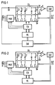
- FIG. 1 shows an example of a calibration method that is not claimed.
- FIGS. 2 and 3 show two preferred configurations of the method according to the invention. The same elements are provided with the same reference symbols. The basic elements for carrying out the method according to the invention are the same in the figures.
- the converter contains the weighted capacity network CN with the capacitances C0 to Cn, to which switches are assigned in a switch network SN.
- the output, ie the summation point SP of the weighted capacitance network CN is connected to the input of a comparator K which is followed by a successive approximation register SAR.
- the outputs n of the successive approximation register corresponding to the internal, ie redundant number n of bits form the output OUT of the converter on the one hand and, on the other hand, are based on the principle of the converter on the switch network SN and, depending on the exemplary embodiment, on a computing unit RE or on a D / A converter returned with register DAR.
- a time control unit and a calibration logic for carrying out the calibration TCN control both the multiplexor MUX and the switch network SN and are connected to the computing unit RE via data lines, which of course contains memory elements.
- the lowest weighted element, together with measurement terms, is initially regarded as a parameter and the system of equations is calculated as a function of the parameters.
- the sum of all weighted elements is then used as the normalization value and then the value of each weighted element is calculated and stored with respect to the normalization value.
- the example of a calibration method shown in FIG. 1 is particularly suitable for almost binary-weighted networks.
- the output of the D / A converter is connected to register DAR via a coupling capacitance CK with the summation point SP of the weighted network CN.
- Data exchange with the computing unit is possible via data lines.
- the inputs of the DAR are the outputs of the successive approximation register SAR.
- a capacity to be examined is identical to the sum of all smaller capacities plus an error term.
- Each of the capacitances C1 to Cn is compared step by step with the sum of the lower weighted elements and the Error term measured. This method is carried out with the aid of the elements shown in FIG. 1, the computing unit RE storing the values or parameters of each step. For this purpose, the capacity to be examined, the lower weighted capacities and the error term are recorded. After completing all steps, the following system of equations GS 1 results:
- the deviations of the capacitances Ci from an ideal value to be assigned to them can also be represented if this is known in advance.
- the value of each bit corresponding to the assigned capacitance with respect to the overall network is known.
- the network CN is a redundant one Network that works with code overlap, a code conversion from the redundant code into the binary code is still required. This code conversion takes place, for example, with the aid of the method described by Boyacigiller with simultaneous error correction.
- each capacity or each weighted element is represented as the sum of a number of lower-order capacities or weighted elements.
- a prerequisite for carrying out this exemplary embodiment of the invention is that this is also possible in reality. This means that no capacity or none of the weighted elements may be larger than the sum of all smaller capacities or weighted elements. In practice, however, this does not mean a significant restriction, since a good translator must comply with this condition in any case in order to avoid missing gaps.
- each of the capacitances to be examined is compared with lower-weighted capacities, corresponding to the example according to FIG. 1, and the GS2 equation system is obtained:
- the coefficients Dij are known.
- the values for the capacitances Ci can then be calculated from the equation system GS 2 with the aid of the computing unit RE. Since the coefficients Dij can only assume the values 0 or 1, the result of the calculation is only accurate to a limited extent. However, since at least one quantization inaccuracy must be taken into account in principle with every self-calibration method, this restriction is not of great importance. In addition, more internal bits can be provided in a redundant converter than the required number of binary bits.
- each weighted element i.e. gradually compare each capacity with the sum of all lower-value capacities.
- the output of the successive approximation register SAR leads into the D / A converter with register DAR, which is connected to the computing unit RE via data lines.
- the output of DAR is connected to another input of the multiplexer MUX.
- the quantities dUi in the GS3 system of equations are dimensionless, since they relate to the full-scale or refer to the standard voltage.
- the capacitance values Ci can be calculated with the aid of the computing unit RE.
- the property is exploited here that the A / D converter to be calibrated can itself be used to quantize the error voltages dUi.
- the result of the first run of this calibration method according to the invention is also comparatively imprecise due to the relatively imprecise converter.
- the accuracy of a converter can be improved iteratively using the method according to the invention.
- This self-calibration method according to the invention with iterative improvement of the accuracy is carried out in such a way that in the first pass the error voltages dUi are determined with the still relatively imprecise converter, the capacitances Ci are determined and the error voltages dUi are quantized.
- the next iteration of the iterative process, a pure calculation run, the results obtained in the first run are used in order to be able to determine the capacities more precisely, etc.
- the self-calibration procedure ends when a deviation criterion is met between the results of two runs.
- This deviation criterion results, for example, from the required accuracy of the converter or the possible calculation accuracy for the elements, taking parasitic properties into account.
- a fixed number of calculation loops for example 10 or 15, is specified as the criterion.
- the self-calibration process according to the invention with an iterative method converges quickly in practice and in theory to an exact solution, the quality of which essentially depends on the parameters which also determine the quality in the case of converters known from the prior art, namely e.g. Resolution, offset and noise. Due to the iterative process, an extremely high accuracy of the converter can be achieved, although the adaptation tolerances of the converter may be a few percent.
- the advantage of the method according to the invention described on the basis of the two exemplary embodiments according to FIG. 2 and FIG. 3 is that it is suitable, with no or only slight restrictions, for redundant, weighted networks and thus for converters which operate on the principle of code overlap.
- the method according to the invention is also easy to implement for these converters.
- a further advantage arises from the fact that only a separate calibration D / A converter is required for the self-calibration method according to the invention is. However, there may be a higher computing effort than with comparable self-calibration methods for binary-weighted networks.
- Computation methods are suitable for the solution of the system of equations determined by measurement in the described methods.
- the exemplary embodiment according to FIG. 2 leads to an exact solution by means of matrix inversion.
- it is expedient to provide start values for the calculation these start values advantageously representing the ideal values of the weighted elements.
- every average person skilled in the art will provide, for example, a ROM as the starting value memory and a RAM or EEPROM for the correction values or the determined capacity values.
Landscapes
- Physics & Mathematics (AREA)
- Nonlinear Science (AREA)
- Engineering & Computer Science (AREA)
- Theoretical Computer Science (AREA)
- Analogue/Digital Conversion (AREA)
Claims (7)
- Procédé de calibrage pour des convertisseurs analogique/numérique et numérique/analogique redondants comportant un réseau pondéré et une unité de correction d'erreurs, caractérisé par un équilibrage automatique, lors duquel, au moyen d'une mesure sur n pas, chacun de n éléments pondérés (C1 à Cn) est déterminé, hormis l'élément possédant la pondération la plus faible, en fonction d'éléments pondérés respectivement avec une pondération plus faible et ensuite, chaque élément pondéré (C0 à Cn) est calculé en rapport avec la somme (FS) de tous les éléments pondérés, au moyen d'une unité de calcul (RE), en fonction des résultats de mesure (Dij) et est mémorisé, auquel cas, on prévoit de façon détaillée les étapes opératoires suivantes :a) pas-à-pasa1) on détermine chaque élément pondéré (C1 à Cn), hormis l'élément (CO) du réseau qui possède la pondération la plus faible, sous la forme d'une somme de tous les éléments pondérés avec une pondération plus faible, multipliés chacun par un coefficient numérique (Dij), eta2) on mémorise temporairement les paramètres,b) la pondération de chaque élément pondéré (C0 à Cn) est calculée à l'aide de l'unité de calcul (R1) à partir des paramètres mémorisés temporairement,c) la pondération de chaque élément pondéré est réalisée, par rapport à la somme de pondération (FS) de tous les éléments pondérés (C0 à Cn) du réseau, et est mémorisée.
- Procédé de calibrage pour des convertisseurs analogique/numérique et numérique/analogique redondants comportant un réseau pondéré et une unité de correction d'erreurs, caractérisé par un équilibrage automatique, lors duquel, au moyen d'une mesure sur n pas, chacun de n éléments pondérés (C1 à Cn) est déterminé, hormis l'élément possédant la pondération la plus faible, en fonction d'éléments pondérés respectivement avec une pondération plus faible et ensuite, chaque élément pondéré (C0 à Cn) est calculé en rapport avec la somme (FS) de tous les éléments pondérés, au moyen d'une unité de calcul (RE), en fonction des résultats de mesure (dVi) et est mémorisé, auquel cas, on prévoit de façon détaillée les étapes opératoires suivantes :a) pas-à-pasa1) on détermine une tension de défaut (dUi) ou un courant de défaut en rapport avec le quotient entre chaque élément pondéré (C1 à Cn) - hormis l'élément (CO) pondéré avec la pondération la plus faible - du réseau, et la somme de pondération de tous les éléments pondérés avec une pondération respectivement plus faible, eta2) on mémorise temporairement les paramètres,b) la pondération de chaque élément pondéré (C0 à Cn) est calculée à l'aide de l'unité de calcul à partir des paramètres mémorisés temporairement, et le résultat est mémorisé temporairement,c) les résultats mémorisés temporairement sont comparés, élément par élément, aux résultats, éventuellement mémorisés temporairement lors du cycle précédent, des pondérations calculées,d) lorsqu'un critère est satisfait, les pondérations calculées des éléments pondérés (C0 à Cn) sont mémorisées temporairement, ete) la pondération de chaque élément pondéré est formée, en rapport avec la somme des poids de tous les éléments pondérés (C0 à Cn) du réseau, et est mémorisée et la procédure de calibrage est arrêtée,f) le calcul des éléments pondérés conformément l'étape b) est répété avec les pondérations calculées lors de l'étape b) et mémorisées temporairement.
- Procédé suivant la revendication 2, caractérisé par le fait que les tensions de défaut ou les courants de défaut sont déterminées et quantifiées au moyen du convertisseur devant être calibré, lui-même.
- Procédé suivant la revendication 2 ou 3, caractérisé par le fait qu'un nombre fixe de cycles est prédéterminé comme critère.
- Procédé suivant la revendication 2 ou 3, caractérisé par le fait qu'une valeur d'écart entre les résultats de deux cycles est prédéterminée en tant que critère.
- Procédé suivant les revendications 2 à 5, caractérisé par le fait que lors du premier cycle de calibrage, des valeurs de départ de pondération pour chaque élément pondéré (C0 à Cn) sont prélevées d'une mémoire de valeurs fixes.
- Procédé suivant les revendications 1 à 6, caractérisé par le fait que la pondération calculée de chaque élément pondéré (C0 à Cn) est mémorisée sous la forme d'un mot possédant une largeur en bits de redondance.
Applications Claiming Priority (2)
| Application Number | Priority Date | Filing Date | Title |
|---|---|---|---|
| DE3742361 | 1987-12-14 | ||
| DE3742361 | 1987-12-14 |
Publications (2)
| Publication Number | Publication Date |
|---|---|
| EP0320642A1 EP0320642A1 (fr) | 1989-06-21 |
| EP0320642B1 true EP0320642B1 (fr) | 1994-10-05 |
Family
ID=6342579
Family Applications (1)
| Application Number | Title | Priority Date | Filing Date |
|---|---|---|---|
| EP88119236A Expired - Lifetime EP0320642B1 (fr) | 1987-12-14 | 1988-11-18 | Procédé de calibration pour convertisseurs analogique-numérique ou numérique-analogique redondants à réseau pondéré |
Country Status (5)
| Country | Link |
|---|---|
| US (1) | US4970514A (fr) |
| EP (1) | EP0320642B1 (fr) |
| JP (1) | JP3224808B2 (fr) |
| AT (1) | ATE112655T1 (fr) |
| DE (1) | DE3851747D1 (fr) |
Cited By (1)
| Publication number | Priority date | Publication date | Assignee | Title |
|---|---|---|---|---|
| DE10314189A1 (de) * | 2003-03-28 | 2004-10-21 | Infineon Technologies Ag | Verfahren und Vorrichtung zur Kalibrierung eines gewichteten Netzwerks |
Families Citing this family (34)
| Publication number | Priority date | Publication date | Assignee | Title |
|---|---|---|---|---|
| EP0536504B1 (fr) * | 1991-08-15 | 1997-11-19 | Texas Instruments Incorporated | Calibration d'un système composé d'une serie d'étapes reconfigurables |
| US6169502B1 (en) * | 1998-05-08 | 2001-01-02 | Cirrus Logic, Inc. | Pipelined analog-to-digital converter (ADC) systems, methods, and computer program products |
| US6229465B1 (en) * | 1999-04-30 | 2001-05-08 | International Business Machines Corporation | Built in self test method and structure for analog to digital converter |
| DE19936327C2 (de) * | 1999-08-02 | 2003-04-24 | Infineon Technologies Ag | Verfahren und Vorrichtung zur Durchführung von ratiometrischen Messungen unter Verwendung eines Analog/Digital- oder eines Digital/Analog-Umsetzers, Analog/Digital- oder Digital/Analog-Umsetzer, und Verfahren zum Betreiben eines Analog/Digital- oder Digital/Analog-Umsetzers |
| US6424276B1 (en) * | 1999-09-09 | 2002-07-23 | Cirrus Logic, Inc. | Successive approximation algorithm-based architectures and systems |
| US6348885B1 (en) * | 1999-09-09 | 2002-02-19 | Cirrus Logic, Inc. | System and method for digitally calibrating an analog-to-digital converter |
| US6292125B1 (en) | 1999-09-29 | 2001-09-18 | Lsi Logic Corporation | Digital-to-analog converter using weights stored in a weight table |
| US6563444B2 (en) * | 2001-03-30 | 2003-05-13 | Iowa State University Research Foundation, Inc. | Apparatus for and method of performing a conversion operation |
| US6975950B2 (en) * | 2003-12-18 | 2005-12-13 | Analog Devices, Inc. | Variable resolution digital calibration |
| WO2007041378A1 (fr) * | 2005-09-30 | 2007-04-12 | Cirrus Logic, Inc. | Etalonnage d'un convertisseur analogique-numerique par approximations successives pour systeme a nombres redondants |
| DE102006029734B4 (de) * | 2006-06-28 | 2014-02-06 | Lantiq Deutschland Gmbh | Binäres Netzwerk für einen nach dem Prinzip der sukzessiven Approximation arbeitenden Analog-Digital-Wandler mit redundantem Gewicht |
| KR100845134B1 (ko) * | 2006-11-06 | 2008-07-09 | 삼성전자주식회사 | 디지털 자동 보정기능을 가지는 파이프 라인아날로그-디지털 변환기 및 그것의 디지털 보정방법 |
| US7733258B2 (en) | 2008-09-30 | 2010-06-08 | Freescale Semiconductor, Inc. | Data conversion circuitry for converting analog signals to digital signals and vice-versa and method therefor |
| US7868796B2 (en) * | 2008-09-30 | 2011-01-11 | Freescale Semiconductor, Inc. | Self-calibrating data conversion circuitry and method therefor |
| US7876254B2 (en) * | 2008-09-30 | 2011-01-25 | Freescale Semiconductor, Inc. | Data conversion circuitry having successive approximation circuitry and method therefor |
| US7880650B2 (en) | 2008-09-30 | 2011-02-01 | Freescale Semiconductor, Inc. | Method and apparatus for testing data converter |
| US7868795B2 (en) * | 2008-09-30 | 2011-01-11 | Freescale Semiconductor, Inc. | Data conversion circuitry with an extra successive approximation step and method therefor |
| US8111178B2 (en) * | 2009-11-26 | 2012-02-07 | Mediatek Inc. | Calibration method and related calibration apparatus for capacitor array |
| US8717214B1 (en) | 2011-02-08 | 2014-05-06 | Maxim Integrated Products, Inc. | Precision sub-RADIX2 DAC with linearity calibration |
| US8330634B2 (en) | 2011-02-08 | 2012-12-11 | Maxim Integrated Products, Inc. | Precision sub-radix2 DAC with linearity calibration |
| TWI545903B (zh) * | 2011-03-17 | 2016-08-11 | 安娜卡敦設計公司 | 類比轉數位轉換器(adc)之校正 |
| US8477052B2 (en) | 2011-04-05 | 2013-07-02 | Freescale Semiconductor, Inc. | Method and apparatus for self-test of successive approximation register (SAR) A/D converter |
| DE102011110115B4 (de) * | 2011-08-15 | 2015-02-26 | Texas Instruments Deutschland Gmbh | Vorrichtung und Verfahren zum Messen der DNL eines SAR ADC |
| DE102014200624B3 (de) | 2014-01-15 | 2015-03-12 | Fraunhofer-Gesellschaft zur Förderung der angewandten Forschung e.V. | Digital-Analog-Wandler, Analog-Digital-Wandlern und Verfahren zur Kalibrierung eines Digital-Analog-Wandlers |
| JP6372102B2 (ja) * | 2014-03-10 | 2018-08-15 | 株式会社ソシオネクスト | アナログデジタル変換回路 |
| US9337860B1 (en) | 2014-07-03 | 2016-05-10 | Maxim Integrated Products, Inc. | Precision sub-RADIX2 DAC with analog weight based calibration |
| US9673832B2 (en) * | 2015-05-15 | 2017-06-06 | Mediatek Inc. | Successive approximation analog-to-digital converter and accuracy improving method thereof |
| TWI556585B (zh) * | 2015-06-11 | 2016-11-01 | 矽創電子股份有限公司 | 類比至數位轉換裝置及相關的校正方法及校正模組 |
| US9473164B1 (en) * | 2015-06-26 | 2016-10-18 | Freescale Semiconductor, Inc. | Method for testing analog-to-digital converter and system therefor |
| US9692441B2 (en) * | 2015-06-30 | 2017-06-27 | Renesas Electronics Corporation | AD converter and AD conversion method |
| JP6703814B2 (ja) | 2015-08-28 | 2020-06-03 | ルネサスエレクトロニクス株式会社 | Ad変換器及びad変換装置 |
| JP6741464B2 (ja) * | 2016-04-27 | 2020-08-19 | ラピスセミコンダクタ株式会社 | 半導体装置、電池監視システム、及びテスト方法 |
| CN107248864B (zh) * | 2017-06-08 | 2020-09-08 | 中国电子科技集团公司第二十四研究所 | 基于权重校准的高精度模数转换器及转换方法 |
| US11196437B1 (en) | 2020-12-01 | 2021-12-07 | Infineon Technologies Ag | System and method for testing an analog-to-digital converter |
Family Cites Families (6)
| Publication number | Priority date | Publication date | Assignee | Title |
|---|---|---|---|---|
| US4318085A (en) * | 1978-06-01 | 1982-03-02 | The Bendix Corporation | Method and apparatus for conversion of signal information between analog and digital forms |
| US4336526A (en) * | 1978-08-04 | 1982-06-22 | Intersil, Inc. | Successive approximation analog-to-digital converter using non-binary series |
| JPS56122524A (en) * | 1980-03-04 | 1981-09-26 | Nippon Telegr & Teleph Corp <Ntt> | Digital-to-analog converter |
| US4399426A (en) * | 1981-05-04 | 1983-08-16 | Tan Khen Sang | On board self-calibration of analog-to-digital and digital-to-analog converters |
| US4451821A (en) * | 1981-11-03 | 1984-05-29 | Texas Instruments Incorporated | Combination of analog to digital converter and error correction circuit |
| JPS60212030A (ja) * | 1984-04-04 | 1985-10-24 | Matsushita Electric Ind Co Ltd | デジタル・アナログ変換回路 |
-
1988
- 1988-11-18 AT AT88119236T patent/ATE112655T1/de not_active IP Right Cessation
- 1988-11-18 EP EP88119236A patent/EP0320642B1/fr not_active Expired - Lifetime
- 1988-11-18 DE DE3851747T patent/DE3851747D1/de not_active Expired - Fee Related
- 1988-12-12 JP JP31480988A patent/JP3224808B2/ja not_active Expired - Fee Related
- 1988-12-14 US US07/284,300 patent/US4970514A/en not_active Expired - Lifetime
Non-Patent Citations (1)
| Title |
|---|
| IEEE TRANSACTIONS ON CIRCUITS AND SYSTEMS, Band CAS-30, Nr. 3, März 1983, Seiten 188-190; H.-S. LEE et al.: "Self-calibration technique for A/D converters" * |
Cited By (3)
| Publication number | Priority date | Publication date | Assignee | Title |
|---|---|---|---|---|
| DE10314189A1 (de) * | 2003-03-28 | 2004-10-21 | Infineon Technologies Ag | Verfahren und Vorrichtung zur Kalibrierung eines gewichteten Netzwerks |
| DE10314189B4 (de) * | 2003-03-28 | 2006-05-11 | Infineon Technologies Ag | Verfahren und Vorrichtung zur Kalibrierung eines gewichteten Netzwerks |
| US7046178B2 (en) | 2003-03-28 | 2006-05-16 | Infineon Technologies Ag | Method and device for the calibration of a weighted network |
Also Published As
| Publication number | Publication date |
|---|---|
| US4970514A (en) | 1990-11-13 |
| EP0320642A1 (fr) | 1989-06-21 |
| ATE112655T1 (de) | 1994-10-15 |
| JPH01194609A (ja) | 1989-08-04 |
| JP3224808B2 (ja) | 2001-11-05 |
| DE3851747D1 (de) | 1994-11-10 |
Similar Documents
| Publication | Publication Date | Title |
|---|---|---|
| EP0320642B1 (fr) | Procédé de calibration pour convertisseurs analogique-numérique ou numérique-analogique redondants à réseau pondéré | |
| EP0360914B1 (fr) | Convertisseurs A/N et N/A à auto-étalonnage | |
| DE102017102501B4 (de) | ADC-Hintergrundkalibration mit zweifacher Umsetzung | |
| DE3002208C2 (fr) | ||
| DE3634855C1 (de) | Kapazitive Messanordnung zur Bestimmung von Kraeften und/oder Druecken | |
| DE3642070A1 (de) | Verfahren zum abgleichen einer mehrzahl von kapazitaeten in einem monolitischen integrierten schaltkreis | |
| DE102009010155B4 (de) | Digitales Trimmen von (SAR-)ADCs | |
| DE2059933C3 (de) | Digital-Analog-Umsetzer | |
| DE2614916A1 (de) | Konverter zur codeumwandlung | |
| DE102017129062B4 (de) | Analog/Digital-Umsetzer mit Hintergrundkalibrierungstechniken | |
| DE10314189B4 (de) | Verfahren und Vorrichtung zur Kalibrierung eines gewichteten Netzwerks | |
| DE19936327C2 (de) | Verfahren und Vorrichtung zur Durchführung von ratiometrischen Messungen unter Verwendung eines Analog/Digital- oder eines Digital/Analog-Umsetzers, Analog/Digital- oder Digital/Analog-Umsetzer, und Verfahren zum Betreiben eines Analog/Digital- oder Digital/Analog-Umsetzers | |
| DE102015107885A1 (de) | Fehlermessung und Kalibrierung von Analog-Digital-Umsetzern | |
| DE2922550A1 (de) | Verfahren und geraet zur umsetzung von analog- in digitaldaten und umgekehrt | |
| EP0400179A1 (fr) | Méthode et dispositif de test interne en parallèle de mémoires à semi-conducteurs | |
| EP0360919B1 (fr) | Procédé de détermination et de traitement de valeurs de correction pour des convertisseurs A/N et N/A à auto-étalonnage et unité de calcul pour la mise en fonction du procédé | |
| DE102016108796B4 (de) | Korrigierte Temperatursensormessung | |
| DE102014200624B3 (de) | Digital-Analog-Wandler, Analog-Digital-Wandlern und Verfahren zur Kalibrierung eines Digital-Analog-Wandlers | |
| DE3810456A1 (de) | Verfahren zur verringerung eines fehlers eines messumformers und einrichtung hierzu | |
| DE3725663C2 (fr) | ||
| DE4009383C2 (fr) | ||
| DE102019113970A1 (de) | Erkennung von adressfehlern | |
| DE2852095C2 (de) | Analog-Digital-Wandlung mit stufenweiser Approximation eines Digitalsignals an ein umzusetzendes Analogsignal | |
| DE3050456C2 (fr) | ||
| DE102020207895A1 (de) | Verfahren und Sensorsystem zum Zuordnen eines gemessenen Druckwerts zu einem Rohmesswert eines kapazitiven Drucksensors |
Legal Events
| Date | Code | Title | Description |
|---|---|---|---|
| PUAI | Public reference made under article 153(3) epc to a published international application that has entered the european phase |
Free format text: ORIGINAL CODE: 0009012 |
|
| AK | Designated contracting states |
Kind code of ref document: A1 Designated state(s): AT BE CH DE FR GB IT LI LU NL SE |
|
| 17P | Request for examination filed |
Effective date: 19890706 |
|
| 17Q | First examination report despatched |
Effective date: 19900704 |
|
| GRAA | (expected) grant |
Free format text: ORIGINAL CODE: 0009210 |
|
| AK | Designated contracting states |
Kind code of ref document: B1 Designated state(s): AT BE CH DE FR GB IT LI LU NL SE |
|
| PG25 | Lapsed in a contracting state [announced via postgrant information from national office to epo] |
Ref country code: BE Effective date: 19941005 Ref country code: NL Effective date: 19941005 |
|
| REF | Corresponds to: |
Ref document number: 112655 Country of ref document: AT Date of ref document: 19941015 Kind code of ref document: T |
|
| PGFP | Annual fee paid to national office [announced via postgrant information from national office to epo] |
Ref country code: AT Payment date: 19941027 Year of fee payment: 7 |
|
| REF | Corresponds to: |
Ref document number: 3851747 Country of ref document: DE Date of ref document: 19941110 |
|
| PG25 | Lapsed in a contracting state [announced via postgrant information from national office to epo] |
Ref country code: LU Free format text: LAPSE BECAUSE OF NON-PAYMENT OF DUE FEES Effective date: 19941130 Ref country code: LI Effective date: 19941130 Ref country code: CH Effective date: 19941130 |
|
| ITF | It: translation for a ep patent filed |
Owner name: STUDIO JAUMANN |
|
| PG25 | Lapsed in a contracting state [announced via postgrant information from national office to epo] |
Ref country code: SE Effective date: 19950105 |
|
| GBT | Gb: translation of ep patent filed (gb section 77(6)(a)/1977) |
Effective date: 19941221 |
|
| ET | Fr: translation filed | ||
| NLV1 | Nl: lapsed or annulled due to failure to fulfill the requirements of art. 29p and 29m of the patents act | ||
| REG | Reference to a national code |
Ref country code: CH Ref legal event code: PL |
|
| PLBE | No opposition filed within time limit |
Free format text: ORIGINAL CODE: 0009261 |
|
| STAA | Information on the status of an ep patent application or granted ep patent |
Free format text: STATUS: NO OPPOSITION FILED WITHIN TIME LIMIT |
|
| 26N | No opposition filed | ||
| PG25 | Lapsed in a contracting state [announced via postgrant information from national office to epo] |
Ref country code: AT Effective date: 19951118 |
|
| REG | Reference to a national code |
Ref country code: GB Ref legal event code: IF02 |
|
| APAH | Appeal reference modified |
Free format text: ORIGINAL CODE: EPIDOSCREFNO |
|
| PG25 | Lapsed in a contracting state [announced via postgrant information from national office to epo] |
Ref country code: IT Free format text: LAPSE BECAUSE OF NON-PAYMENT OF DUE FEES;WARNING: LAPSES OF ITALIAN PATENTS WITH EFFECTIVE DATE BEFORE 2007 MAY HAVE OCCURRED AT ANY TIME BEFORE 2007. THE CORRECT EFFECTIVE DATE MAY BE DIFFERENT FROM THE ONE RECORDED. Effective date: 20051118 |
|
| PGFP | Annual fee paid to national office [announced via postgrant information from national office to epo] |
Ref country code: FR Payment date: 20061124 Year of fee payment: 19 |
|
| PGFP | Annual fee paid to national office [announced via postgrant information from national office to epo] |
Ref country code: GB Payment date: 20061127 Year of fee payment: 19 |
|
| PGFP | Annual fee paid to national office [announced via postgrant information from national office to epo] |
Ref country code: DE Payment date: 20070115 Year of fee payment: 19 |
|
| GBPC | Gb: european patent ceased through non-payment of renewal fee |
Effective date: 20071118 |
|
| PG25 | Lapsed in a contracting state [announced via postgrant information from national office to epo] |
Ref country code: DE Free format text: LAPSE BECAUSE OF NON-PAYMENT OF DUE FEES Effective date: 20080603 |
|
| REG | Reference to a national code |
Ref country code: FR Ref legal event code: ST Effective date: 20080930 |
|
| PG25 | Lapsed in a contracting state [announced via postgrant information from national office to epo] |
Ref country code: GB Free format text: LAPSE BECAUSE OF NON-PAYMENT OF DUE FEES Effective date: 20071118 |
|
| PG25 | Lapsed in a contracting state [announced via postgrant information from national office to epo] |
Ref country code: FR Free format text: LAPSE BECAUSE OF NON-PAYMENT OF DUE FEES Effective date: 20071130 |