EP0305992B1 - Verarbeitungsanordnung zum Einfügen oder Ausblenden von Kanälen - Google Patents
Verarbeitungsanordnung zum Einfügen oder Ausblenden von Kanälen Download PDFInfo
- Publication number
- EP0305992B1 EP0305992B1 EP88114191A EP88114191A EP0305992B1 EP 0305992 B1 EP0305992 B1 EP 0305992B1 EP 88114191 A EP88114191 A EP 88114191A EP 88114191 A EP88114191 A EP 88114191A EP 0305992 B1 EP0305992 B1 EP 0305992B1
- Authority
- EP
- European Patent Office
- Prior art keywords
- speed data
- clock signal
- data
- low
- circuit
- Prior art date
- Legal status (The legal status is an assumption and is not a legal conclusion. Google has not performed a legal analysis and makes no representation as to the accuracy of the status listed.)
- Expired - Lifetime
Links
Images




Classifications
-
- H—ELECTRICITY
- H04—ELECTRIC COMMUNICATION TECHNIQUE
- H04J—MULTIPLEX COMMUNICATION
- H04J3/00—Time-division multiplex systems
- H04J3/02—Details
- H04J3/08—Intermediate station arrangements, e.g. for branching, for tapping-off
Definitions
- the present invention relates to a drop/insert processing circuit
- a drop/insert processing circuit comprising a clock signal generating circuit for dividing said high-frequency clock signal into a low-frequency clock signal; a shift register for serially receiving and shifting high speed data in response to said high-frequency clock signal; low speed data insertion control means for inserting, in response to said low-frequency clock signal and a data insertion control signal, low speed data in said high speed data passing through said shift register; and low speed data dropping means for dropping, in response to said low-frequency clock signal, low speed data from the shift register; said low-frequency clock signal having one enable period corresponding to one of said channels in the frame of said high speed data and being synchronous with at least one of the outputs of said low speed data dropping means; said clock signal generating circuit and said shift register are used in common by both said low speed data insertion control means and said low speed data dropping means, and said shift register comprises a plurality of first latching circuits for serially receiving and shifting high speed data in response to said high
- a synchronous optical network As a broadband subscriber network, a synchronous optical network (SONET) has been developed in which a broadband subscriber loop system based on a single-mode fiber is employed, and high speed data is run through the loop. Terminal units dealing with low speed data are connected to the broadband subscriber loop, and therefore, drop/insert processing circuits must be connected between the high speed data loop and the low speed data terminal units, for dropping data from the loop or for inserting data into the loop.
- SONET synchronous optical network
- An object of the present invention is to reduce the circuit scale of a drop/insert processing circuit and to simplify the control of the drop/insert processing.
- the drop/insert processing circuit initially defined is characterized in that the insertion control means is arranged for inserting said low speed data into a channel specified by said data insertion control signal; said low speed data insertion control means comprises a plurality of control circuits for passing said low-frequency clock signal in response to said data insertion control signal, and a plurality of low speed data inserting switches each being connected to one of said control circuits and connected between two adjacent said first latching circuits, to selectively output either said high speed data and said low speed data in response to said low-frequency clock signal passed through said control circuit; said low speed data dropping means comprises a plurality of second latching circuits, respectively connected to outputs of said first latching circuits, for incorporating and outputting the corresponding one of outputs of said first latching circuits in response to said low-frequency clock signal, in order to drop low speed data, and each of said first latching circuits except for the final stage latching circuit has two output terminals for providing shifted high speed data, one of said output terminals being connected to
- the data insertion into one or more of the desired channels at the outputs of the necessary stages of the shift register, and the data dropping from one or more of the outputs of the necessary stages can be carried out by a single shift register and a single clock signal generating circuit.
- Figure 1 is a diagram showing an example of a conventional broadband subscriber network used in the field to which the present invention is related.
- LAN local area network
- MAN metropolitan area network
- drop/insert processing circuits 12, 13, 14, and 15 are provided on a data bus 11 in the shape of a loop.
- any arbitrary data on a channel from a series of time-division multiplexed signals flowing through the data bus 11 at a high speed must be dropped into the terminals 16, 17, and so forth, or a signal from the terminals 16, 17 and so forth, inserted at any arbitrary channel through the drop/insert processing circuits.
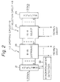
- Figure 2 is a block diagram showing an example of a conventional drop/insert processing circuit.
- a parallel type circuit in which a high speed serial data of, for example, 1.2 Gb/s is once separated or demultiplexed in parallel and then multiplexed.
- series data of 1.2 Gb/s is converted by a demultiplexing circuit 21 into 8-bits parallel data of 150 Mb/s in response to a low-frequency clock signal generated from a synchronization detecting circuit 22.
- the low speed parallel data is then input into an 8:16 distributing circuit 23 having eight 1:2 dropping circuits.
- the distributing circuit 23 receives the 8-bit parallel data and distributes this data into two parts of the 8-bit data through the dropping circuits, and thus the desired channel data is dropped as 8-bit parallel data of 150 Mb/s.
- the data passed through the distributing circuit 23 is input to a 16:8 selecting circuit 24 consisting of eight 2:1 selecting circuits, wherein one or more of the 8-bit parallel data of 150 Mb/s is inserted at desired channels of the signal passing through the 16:8 selecting circuit 24, and then the outputs of the selecting circuit 24 are multiplexed into high speed data of 1.2 Gb/s by a multiplexer 25.
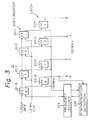
- Figure 3 is a block diagram showing an example of the demultiplexing circuit 25 in the circuit shown in Fig. 2.
- the input data of 1.2 Gb/s consisting of eight channels is sequentially shifted from flip-flops 211-8 to 211-1, which constitute a shift register and data of the respective channels is obtained at the respective inverted outputs of the flip-flops.
- the parallel data obtained at the outputs of the flip-flops 211-1 to 211-8 consists of 8-bit parallel data of 150 Mb/s which is latched and then output by flip-flops 212-8 to 212-1 in response to a low frequency clock signal of 150 MHz.
- the shifted data of 150 Mb/s is sequentially latched at the flip-flops 211-8 to 211-1 and output from the outputs of these flip-flops.
- a frequency divider 213 generates a low-frequency clock signal of 150 MHz based on the 1.2 GHz clock signal and the output of a synchronization detecting circuit 214, and the synchronization detecting circuit 214 generates a synchronization detecting signal which is applied to the frequency divider 213, based on the outputs from the flip-flops 212-8 to 212-1 and the output from the frequency divider 213.
- FIG. 4 is a block diagram showing a shift register type multiplexer (MUX) 25 as an example of a conventional multiplexing circuit.
- MUX shift register type multiplexer
- the corresponding one or more switches 252-6 to 252-0 are driven so that the data of 150 Mb/s is latched in the corresponding one or more flip-flops 551-6 to 551-0, and in response to the 1.2 GHz clock signal, the above-mentioned latched data is sequentially shifted.
- a frequency divider 253 generates the above-mentioned 150 MHz clock signal having a duty ratio of 1:7, based on the 1.2 GHz clock signal.
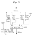
- Figure 5 is a block diagram showing a selector type MUX as another example of a conventional multiplexing circuit.
- flip-flops 254-1 to 254-8 latch the data of 150 Mb/s in response to the 150 MHz clock signal.
- a frequency divider 255 generates the above-mentioned clock signal of 150 MHz based on the 1.2 GHz clock signal, and generates a 3-bit control signal to be applied to a 8:1 selector 256.
- the 8:1 selector 256 sequentially selects the outputs of the flip-flops 254-8 to 254-1 in response to the above-mentioned control signal, so that data of 1.2 Gb/s is obtained.
- Figure 6 is a block diagram showing another example of a drop/insert processing circuit used during research carried out by the present inventors to realize the present invention.
- a control circuit 61 receives a control signal and generates a signal synchronous with a channel from which data is to be dropped.
- the signal passes through an AND gate 62 in response to the 1.2 GHz clock signal and is supplied to a flip-flop (FF) 63, and the flip-flop (FF) 63 latches the data of 1.2 GHz at the timings thereof. Accordingly, dropped data of 150 Mb/s is obtained at the output of the flip-flop (FF) 63.
- a control circuit 65 generates a signal which is synchronous with the channel to which data is to be inserted, and this signal is applied to a 2:1 selecting circuit 64. Accordingly, data is inserted into a desired channel and a flip-flop (FF) 66 outputs high speed data, which is synchronous with the 1.2 GHz clock signal, to a high speed data bus 67.
- Figure 7 is a principal block diagram of the constitution of the present invention.
- the drop/insert processing circuit is used for dropping low speed data (DLD) from high speed data (HD) or inserting low speed data (ILD) into high speed data.
- the high speed data has a frame consisting of a plurality of channels, and each channel is synchronous with a high-frequency clock signal.
- the drop/insert processing circuit comprises a clock signal generating circuit 71, a shift register 72, a low speed data insertion control circuit 73, and a low speed data dropping circuit 74.
- the clock signal generating circuit 71 divides the high-frequency clock signal into a low-frequency clock signal; the shift register 72 serially receives and shifts the high speed data in response to the high-frequency clock signal; the low speed data insertion control means 73 inserts, in response to the low-frequency clock signal and a data insertion control signal, the low speed data into a channel, specified by the data insertion control signal, in the high speed data passing through the shift register; and the low speed data dropping circuit 74 drops, in response to the low-frequency clock signal, low speed data from the shift register.
- the clock signal generating circuit and the shift register are common to both the low speed data insertion control circuit and the low speed data dropping circuit, and therefore, the circuit scale can be reduced and the drop/insert control can be simplified.
- Figure 8 is a block diagram showing the principle of an embodiment of the present invention.
- the drop/insert processing circuit includes a shift register 81.
- the shift register 81 comprises (n+1) first latching circuits 81-1, 81-2, ... and 81-(n+1) for shifting data of f bits/s in response to a clock signal having a frequency f , n data inserting circuits 82-1, 82-2, ... and 82-n each connected between two adjacent first latching circuits, and n data insertion control switches 83-1, 83-2, ... and 83-n each having an output connected to a control input of the corresponding one of the data inserting switches 82-1, 82-2, ... and 82-n.
- the drop/insert processing circuit further includes n second latching circuits 84-1, 84-2, ... and 84-n for incorporating, in response to a second clock signal having a frequency f/n and a duty ratio of 1:(n-1), the outputs of the corresponding first latching circuits 81-2 to 82-(n+1).
- the final stage latching circuit 81-1 is not connected to a second latching circuit and merely outputs serial high speed data.
- the drop/insert processing circuit further includes a clock signal generating circuit 85 for dividing the first clock signal to generate a second clock signal which is synchronous with at least one of the outputs of the second latching circuits 84-1 to 84-n.
- the second clock signal has one enable period corresponding to one of the channels in the frame of the high speed data.
- Each of the data insertion control switches 83-1 to 83-n has an end functioning as a control output and has another input for receiving the second clock signal, to determine whether or not data should be inserted.
- the second clock signal is supplied through a data insertion control switch, which is in the ON state, to a data inserting circuit corresponding to the second clock signal so that the bit corresponding to the data of f/n bits/s is inserted into the corresponding latching circuit, and data of f/n sec is dropped from the second latching circuits.
- Figure 9 is a block diagram showing a practical example of the above described embodiment.
- a shift register type drop/insert processing circuit is illustrated in which 91-0 to 91-8 are flip-flops, which constitute a shift register 90 for shifting data of 1.2 Gb/s in response to the 1.2 GHz clock signal.
- Data inserting switches 92-0 to 92-7 are connected between two adjacent flip-flops 91-0 to 91-8.
- Flip-flops 93-1 to 93-8 latch the inverted outputs of the flip-flops 91-1 to 92-8 in response to a clock signal of 150 MHz with a duty ratio of 1:7.
- a frequency divider 941 generates the above-mentioned 150 MHz clock signal based on both the 1.2 GHz clock signal and the output of a synchronization detecting circuit 942.
- the synchronization detecting circuit 942 establishes a synchronization of the phase of the 150 MHz signal obtained by dividing the 1.2 GHz with the rising of the output of the flip-flop 93-8.
- Each of the data insertion selecting switches 95-0 to 95-7 has one end for receiving the above-mentioned 150 MHz clock signal and another end as a control input of each of the data inserting switches 92-0 to 92-7.
- dropped data of 150 Mb/s is obtained at the outputs of the flip-flops 93-1 to 93-8.
- the data insertion control switch corresponding to the desired channel for example, 95-1
- the 150 MHz clock signal is given as a control signal to the corresponding data inserting switch, for example, 92-1, whereby the data inserting switch 92-1 is turned so that the data input terminal of the flip-flop 91-1 receives the desired bit of the inserting data of 150 Mb/s, in place of the output of the pre-stage flip-flop 91-2.
- the data is inserted into the desired channel and is shifted in response to the 1.2 GHz clock signal, so that the data of 1.2 Gb/s is obtained at the output of the flip-flop 91-0.
- Figure 10 is a timing chart of the multiplexing and the demultiplexing process in the circuit shown in Fig. 9.
- the data 1, 2, 3, ..., and 8 which are sequentially shifted through the shift register 90 in response to the 1.2 GHz clock signal, are demultiplexed by a serial-to-parallel conversion at each rise timing of the 150 MHz clock signal, and immediately before the time of each of the shifts through the shift register, the desired data in the data to be inserted is inserted in response to the rise timing of the 150 MHz clock signal.
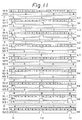
- Figure 11 is a timing chart explaining in more detail the data insertion and data dropping process in the circuit shown in Fig. 9.
- the high speed data of 1.2 GHz input to the flip-flop 91-8 is represented as a cyclic data of 1, 2, ... and 8 consisting of one frame.
- the low speed data 1′, 2′, ... and 7′ of 150 MHz to be inserted as shown in Fig. 10 are represented as A, B, C, D, E, F, G, and H, respectively.
- the low frequency clock signal of 150 MHz is applied, in this example, to the data inserting switches 92-7, 92-6, 92-4, 92-2, and 92-1, as illustrated by solid-line pulses.
- the switches 92-5 and 92-3 do not receive the low frequency clock signal in this example, as illustrated by dotted-line pulses, and the control of the application of the low frequency clock signal to the switches 92-0 to 92-7 is carried out by the control switches 95-0 to 95-7, respectively.
- the low frequency clock signal has a duty ratio of 1:7, i.e., the low frequency clock signal has a high level of one channel period of the high speed data.
- the high level enable period T1 consists of a preceding half period corresponding in time to the last channel of the frame of the input high speed data and a latter half period corresponding in time to the frame of the input high speed data.
- the low speed data of A, B, C, E, G, and H are inserted, in response to the last half period of the low frequency clock signal, to the respective channels corresponding to the clock signal in the high speed data, as illustrated by circles in the figure.
- the high speed data including the inserted data is shifted through the shift register, and accordingly, high speed data of 1.2 GHz, in which each frame consists of the data H, A, B, C, 4, E, 6, and G, is output to the high speed data loop from the final stage flip-flop 91-0.
- the low frequency clock signal of 150 MHz is supplied to all of the second flip-flops 93-1 to 93-8, and therefore, in response to each preceding half period of the low frequency clock signal, the corresponding channel data 1, 2, 3, 4, 5, 6, 7, and 8 is latched by the flip-flops 93-1 to 93-8, respectively.
- the latched data is dropped in parallel from the inverted outputs of the second flip-flops 93-1 to 93-8 as low speed data of 150 Mb/s.
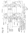
- Figure 12 is a block diagram showing a second embodiment of the present invention.
- a selector type drop/insert processing circuit is illustrated, wherein a shift register 120 includes flip-flops 120-1 to 120-8 for shifting data in response to the 1.2 GHz clock signal; flip-flops 122-1 to 122-8 respectively incorporate the outputs of the flip-flops 120-1 to 120-8 in response to the clock signal of 150 MHz and having a duty ratio of 1:8; flip-flops 121-1 to 121-8 incorporate the inserting parallel data of 150 Mb/s in response to the above-mentioned 150 MHz clock signal; data insertion selecting switches 123-1 to 123-8 selectively output either of the outputs of the flip-flops 122-1 to 122-8 and the outputs of the flip-flops 121-1 to 121-8; and frequency divider 125 forms the above-mentioned 150 MHz clock signal based on both the 1.2 GHz clock signal and the output of the synchronization detecting circuit 126.
- the synchronization detecting circuit 126 synchronizes the phase of the 150 MHz signal, which is obtained by dividing the 1.2 GHz, with the rising of the inverted output of the flip-flop 122-8 and generates a 3-bit control signal to be applied to the 8:1 selector 35.
- the above-described construction enables dropped data of 150 Mb/s to be obtained at the inverted outputs of the flip-flops 122-1 to 122-8.
- the data insertion selecting switch for example, 123-1, corresponding to the desired channel is switched so that, in place of the output of the flip-flop 122-1, the inverted output of the flip-flop 121-1 is input to the 8:1 selector 124.
- the 8:1 selector 124 cyclically selects the output of the switches 123-1 to 123-8 by using the control signal as an address signal, so that the data of 1.2 Gb/s can be obtained at the output thereof.
- the frequency divider part is commonly used in the demultiplexing circuit and the multiplexing circuit part, whereby the conventionally required distributing circuit and selecting circuit become unnecessary, and thus the circuit is simplified.
- the conventionally required distributing circuit and the selecting circuit become unnecessary so that the drop/insert processing circuit can be formed as one body and the circuit scale can be greatly reduced. Further, the low frequency clock signal can be easily generated synchronously with the rise of the data dropping latching circuit, so that the control is simplified.
Landscapes
- Engineering & Computer Science (AREA)
- Computer Networks & Wireless Communication (AREA)
- Signal Processing (AREA)
- Time-Division Multiplex Systems (AREA)
- Small-Scale Networks (AREA)
- Use Of Switch Circuits For Exchanges And Methods Of Control Of Multiplex Exchanges (AREA)
- Communication Control (AREA)
Claims (13)
- Eine Abzweigungs/Einfügungs-Verarbeitungsschaltung zum Abzweigen von Daten mit niedriger Geschwindigkeit von Daten mit hoher Geschwindigkeit oder zum Einfügen von Daten mit niedriger Geschwindigkeit in Daten mit hoher Geschwindigkeit, wobei die Daten mit hoher Geschwindigkeit einen Rahmen aufweisen, der aus einer Vielzahl von Kanälen besteht, wobei jeder Kanal synchron zu einem Hochfrequenz-Taktsignal ist und wobei die Abzweigungs/Einfügungs-Verarbeitungsschaltung umfaßt:
eine Taktsignal-Erzeugungsschaltung (71, 85) zum Teilen des Hochfrequenz-Taktsignals in ein Niederfrequenz-Taktsignal;
ein Schieberegister (72, 81, 90, 120) zum seriellen Empfangen und Verschieben von Daten mit hoher Geschwindigkeit im Ansprechen auf das Hochfrequenz-Taktsignal;
eine Einfügungs-Steuereinrichtung (73, 82, 83; 92, 95; 121, 123) für Daten mit niedriger Geschwindigkeit, um im Ansprechen auf das Niederfrequenz-Taktsignal und ein Daten-Einfügungs-Steuersignal Daten mit niedriger Geschwindigkeit in die durch das Schieberegister laufenden Daten mit hoher Geschwindigkeit einzufügen; und
eine Abzweigungseinrichtung (74, 84, 93, 122) für Daten mit niedriger Geschwindigkeit, um im Ansprechen auf das Niederfrequenz-Taktsignal Daten mit niedriger Geschwindigkeit von dem Schieberegister abzuzweigen;
wobei das Niederfrequenz-Taktsignal eine Aktivierungsperiode aufweist, die einem der Kanäle in dem Rahmen der Daten mit hoher Geschwindigkeit entspricht und synchron zu wenigstens einem der Ausgänge der Abzweigungseinrichtung für Daten mit niedriger Geschwindigkeit ist;
die Taktsignal-Erzeugungsschaltung und das Schieberegister gemeinsam von sowohl der Einfügungs-Steuereinrichtung für Daten mit niedriger Geschwindigkeit als auch von der Abzweigungseinrichtung von Daten mit niedriger Geschwindigkeit verwendet werden; und
das Schieberegister (72, 81, 90, 120) eine Vielzahl von ersten Auffangschaltungen (81-1, ..., 81-n, und 81-(n+1); 91-0, ..., 91-8; 120-1, ..., 120-8) umfaßt, um im Ansprechen auf das Hochfrequenz-Taktsignal Daten mit hoher Geschwindigkeit seriell zu empfangen und zu verschieben,
dadurch gekennzeichnet, daß
die Einfügungs-Steuereinrichtung angeordnet ist, um die Daten mit niedriger Geschwindigkeit in einen von dem Daten-Einfügungs-Steuersignal bezeichneten Kanal einzufügen;
wobei die Einfügungs-Steuereinrichtung (73, 82, 83; 92, 95; 121, 123) für Daten mit niedriger Geschwindigkeit eine Vielzahl von Steuerschaltungen (83-1, 83-2, ... und 83-n, 95-0, ..., 95-7) umfaßt, um das Niederfrequenz-Taktsignal im Ansprechen auf das Daten-Einfügungs-Steuersignal durchzulassen, und eine Vielzahl von Einfügungsschaltern (82-1, 82-2, ..., und 82-n, 92-0, ..., 92-7; 123-1, ..., 123-8) umfaßt, die jeweils mit einer der Steuerschaltungen verbunden sind und zwischen zwei benachbarten der ersten Auffangschaltungen verbunden sind, um selektiv entweder die Daten mit hoher Geschwindigkeit oder die Daten mit niedriger Geschwindigkeit im Ansprechen auf das durch die Steuerschaltung durchgelassene Niederfrequenz-Taktsignal auszugeben;
wobei die Abzweigungseinrichtung (74, 84, 93, 122) für Daten mit niedriger Geschwindigkeit eine Vielzahl von zweiten Auffangschaltungen (84-1, 84-2, ..., 84-n, 93-1, ..., 93-8, 122-1, ..., 122-8) umfaßt, die jeweils mit den Ausgängen der ersten Auffangschaltungen verbunden sind, um den entsprechenden Ausgang der ersten Auffangschaltungen (1-2 bis 1-n) im Ansprechen auf das Niederfrequenz-Taktsignal einzubinden und auszugeben, um die Daten mit niedriger Geschwindigkeit abzuzweigen; und
wobei jede der ersten Auffangschaltungen außer der Auffangschaltung der letzten Stufe zwei Ausgangsanschlüsse zur Bereitstellung von verschobenen Daten mit hoher Geschwindigkeit aufweist, wobei einer der Ausgangsanschlüsse mit dem ersten Eingangsanschluß der Einfügungseinrichtung für Daten mit niedriger Geschwindigkeit verbunden ist und der andere der Ausgangsanschlüsse mit dem Eingang der entsprechenden zweiten Auffangschaltung verbunden ist. - Eine Abzweigungs/Einfügungs-Verarbeitungsschaltung nach Anspruch 1, dadurch gekennzeichnet, daß jeder der Einfügungsschalter für Daten mit niedriger Geschwindigkeit umfaßt: einen ersten Eingangsanschluß zum Empfang von Daten mit hoher Geschwindigkeit, die von einer Vorstufe der ersten Auffangschaltung ausgegeben werden; einen zweiten Eingangsanschluß zum Empfang eines Bits von parallelen Daten der Daten mit niedriger Geschwindigkeit; und einen Ausgangsanschluß zum selektiven Ausgeben entweder der Daten mit hoher Geschwindigkeit oder der Daten mit niedriger Geschwindigkeit im Ansprechen auf das durch die entsprechende Steuerschaltung durchgelassene Niederfrequenz-Taktsignal, wodurch die Daten mit niedriger Geschwindigkeit in einen von dem Steuersignal bezeichneten Kanal eingefügt werden.
- Eine Abzweigungs/Einfügungs-Verarbeitungsschaltung nach Anspruch 1 oder 2, dadurch gekennzeichnet, daß die Daten mit hoher Geschwindigkeit eine Bitrate von f Bits/s und das Hochfrequenz-Taktsignal eine Frequenz von f Hz aufweisen.
- Eine Abzweigungs/Einfügungs-Verarbeitungsschaltung nach Anspruch 3, dadurch gekennzeichnet, daß die Daten mit niedriger Geschwindigkeit eine Bitrate von f/n Bits/s und das Niederfrequenz-Taktsignal eine Frequenz von f/n Hz aufweisen.
- Eine Abzweigungs/Einfügungs-Verarbeitungsschaltung nach Anspruch 4, dadurch gekennzeichnet, daß das Niederfrequenz-Taktsignal ein Tastverhältnis von 1:(n-1) aufweist.
- Eine Abzweigungs/Einfügungs-Verarbeitungsschaltung nach Anspruch 5, dadurch gekennzeichnet, daß die Anzahl der ersten Auffangschaltungen in dem Schieberegister gleich (n+1) ist und die Anzahl der zweiten Auffangschaltungen gleich n ist.
- Eine Abzweigungs/Einfügungs-Verarbeitungsschaltung nach Anspruch 6, dadurch gekennzeichnet, daß die zweiten Auffangschaltungen jeweils Eingangsanschlüsse zum Empfang von Ausgängen der ersten Auffangschaltungen aufweisen, mit der Ausnahme einer letzten Stufe der ersten Auffangschaltungen.
- Eine Abzweigungs/Einfügungs-Verarbeitungsschaltung nach einem der vorangehenden Ansprüche, dadurch gekennzeichnet, daß die letzte Stufe der ersten Auffangschaltungen einen einzigen Ausgang zur Bereitstellung von Ausgangsdaten mit hoher Geschwindigkeit aufweist.
- Eine Abzweigungs/Einfügungs-Verarbeitungsschaltung nach Anspruch 1, dadurch gekennzeichnet, daß die Taktsignal-Erzeugungsschaltung einen Frequenzteiler (941) zum Teilen eines eingegebenen Hochfrequenz-Taktsignals in ein Niederfrequenz-Taktsignal und eine Synchronisations-Erfassungsschaltung (942) zur Herstellung einer Synchronisation zwischen dem Niederfrequenz-Taktsignal und abgezweigten Daten mit niedriger Geschwindigkeit umfaßt.
- Eine Abzweigungs/Einfügungs-Verarbeitungsschaltung nach Anspruch 1, dadurch gekennzeichnet, daß die ersten Auffangschaltungen (81-1, 81-2, ..., und 81-(n+1)) zum Verschieben von Daten von n Bits/s im Ansprechen auf das Hochfrequenz-Taktsignal mit einer Frequenz von f Hz vorgesehen sind;
n zweite Auffangschaltungen (84-1, 84-2, ..., und 84-n) vorgesehen sind, um im Ansprechen auf das Niederfrequenz-Taktsignal mit einer Frequenz von f/n Hz und mit einem Tastverhältnis von 1:(n-1) Ausgänge von allen der ersten Auffangschaltungen (81-2 bis 81-n) bis zur Auffangschaltung (81-1) der letzten Stufe einzubinden;
wobei das Niederfrequenz-Taktsignal durch eine entsprechende der Daten-Einfügungssteuerschaltungen, die sich in dem EIN-Zustand befindet, an den entsprechenden der Daten-Einfügungsschalter geliefert wird, so daß ein Bit entsprechend der Daten von f/n Bits/s an die entsprechende Auffangschaltung eingefügt wird; und
Daten mit f/n Bits/s von den zweiten Auffangschaltungen abgezweigt werden. - Eine Abzweigungs/Einfügungs-Verarbeitungsschaltung nach Anspruch 1, dadurch gekennzeichnet, daß die Einfügungs-Steuereinrichtung (121) für Daten mit niedriger Geschwindigkeit umfaßt:
eine Vielzahl von dritten Auffangschaltungen (121-1 bis 121-8) zum Auffangen von eingegebenen Daten mit niedriger Geschwindigkeit parallel im Ansprechen auf das Niederfrequenz-Taktsignal;
die Vielzahl von zweiten Auffangschaltungen (122-1 bis 122-8) zum jeweiligen Auffangen von Ausgängen der ersten Auffangschaltungen;
die Vielzahl von Einfügungsschaltern (123-1, 123-2, ..., und 123-n) für Daten mit niedriger Geschwindigkeit, die jeweils einen mit einem Ausgang der entsprechenden der zweiten Auffangschaltungen (122-1 bis 122-8) verbundenen ersten Eingangsanschluß, einen mit einem Ausgang der entsprechenden der dritten Auffangschaltungen (121-1 bis 121-8) verbundenen zweiten Eingangsanschluß und einen Ausgangsanschluß aufweist, um im Ansprechen auf das Daten-Einfügungs-Steuersignal irgendeinen der Ausgänge der entsprechenden der dritten oder zweiten Auffangschaltungen auszugeben; und
eine multiplexierende Schaltung (124) mit einer Vielzahl von Eingangsanschlüssen, die jeweils mit dem Ausgangsanschlüssen der Einfügungsschalter für Daten mit niedriger Geschwindigkeit verbunden sind, um Eingangsdaten zur Ermittlung von Ausgangsdaten mit hoher Geschwindigkeit zu multiplexieren; und
wobei die Abzweigungseinrichtung (74) für Daten mit niedriger Geschwindigkeit die zweiten Auffangschaltungen (122-1 bis 122-8) umfaßt, wobei das abgezweigte Signal an Ausgangsanschlüssen davon erhalten wird. - Eine Abzweigungs/Einfügungs-Verarbeitungsschaltung nach Anspruch 11, dadurch gekennzeichnet, daß die Taktsignal-Erzeugungsschaltung einen Frequenzteiler (125) zum Teilen eines eingegebenen Hochfrequenz-Taktsignals in ein Niederfrequenz-Taktsignal und eine Synchronisations-Erfassungsschaltung (126) zur Herstellung einer Synchronisation zwischen dem Niederfrequenz-Taktsignal und den abgezweigten Daten mit niedriger Geschwindigkeit umfaßt.
- Eine Abzweigungs/Einfügungs-Verarbeitungsschaltung nach Anspruch 1, dadurch gekennzeichnet, daß:
das Schieberegister (120) n erste Auffangschaltungen (120-1, 120-2, ..., und 120-8) umfaßt, um im Ansprechen auf ein erstes Taktsignal mit einer Frequenz von f Hz Daten mit f Bits/s zu verschieben;
n dritte Auffangschaltungen (121-1, 121-2, ... und 121-8) vorgesehen sind, um im Ansprechen auf das zweite Taktsignal parallele Daten von f/n Bits/Sek. einzubinden;
wobei die Daten-Einfügungs-Wahlschalter (123-1, 123-2, ..., und 123-8) angeordnet sind, um entweder Ausgänge der zweiten Auffangschaltungen oder Ausgänge der dritten Auffangschaltungen zu wählen;
wobei die Taktsignal-Erzeugungsschaltung (125 und 126) angeordnet ist, um das Niederfrequenz-Taktsignal, welches zumindest zu einem der Ausgänge der zweiten Auffangschaltungen synchron ist, zu erzeugen, und um ein Adreßsignal zur sequentiellen Auswahl von Ausgängen der Daten-Einfügungs-Wählschalter mit einer Frequenz f zu erzeugen; und
ein n:1 Wähler (124) vorgesehen ist, um Ausgänge der Daten-Einfügungs-Wählschalter im Ansprechen auf ein Adreßsignal von der Taktsignal-Erzeugungsschaltung sequentiell zu wählen und auszugeben; und
wobei abgezweigte Daten mit f/n Bits/Sek. von dem Ausgang der zweiten Auffangschaltungen (122-1 bis 122-8) erhalten werden und multiplexierte Daten mit f Bits/Sek. von dem Ausgang des n:1 Wählers erhalten werden.
Applications Claiming Priority (2)
| Application Number | Priority Date | Filing Date | Title |
|---|---|---|---|
| JP62215095A JPS6460035A (en) | 1987-08-31 | 1987-08-31 | Branching/inserting circuit |
| JP215095/87 | 1987-08-31 |
Publications (3)
| Publication Number | Publication Date |
|---|---|
| EP0305992A2 EP0305992A2 (de) | 1989-03-08 |
| EP0305992A3 EP0305992A3 (de) | 1991-02-27 |
| EP0305992B1 true EP0305992B1 (de) | 1994-08-17 |
Family
ID=16666670
Family Applications (1)
| Application Number | Title | Priority Date | Filing Date |
|---|---|---|---|
| EP88114191A Expired - Lifetime EP0305992B1 (de) | 1987-08-31 | 1988-08-31 | Verarbeitungsanordnung zum Einfügen oder Ausblenden von Kanälen |
Country Status (5)
| Country | Link |
|---|---|
| US (1) | US4935920A (de) |
| EP (1) | EP0305992B1 (de) |
| JP (1) | JPS6460035A (de) |
| CA (1) | CA1291831C (de) |
| DE (1) | DE3851109T2 (de) |
Families Citing this family (13)
| Publication number | Priority date | Publication date | Assignee | Title |
|---|---|---|---|---|
| JP2603717B2 (ja) * | 1989-03-09 | 1997-04-23 | 三菱電機株式会社 | サイクリックデータ伝送方法 |
| US5214651A (en) * | 1989-05-11 | 1993-05-25 | Alcatel Network Systems, Inc. | Sonet transmit signaling translator |
| US5134614A (en) * | 1989-05-11 | 1992-07-28 | Alcatel Network Systems, Inc. | Sonet receive signaling translator |
| DE3924283A1 (de) * | 1989-07-22 | 1991-01-31 | Standard Elektrik Lorenz Ag | Schaltungsanordnung zur durchschaltung eines digitalen dienstkanals in einer richtfunk-zwischenstelle |
| GB9005723D0 (en) * | 1990-03-14 | 1990-05-09 | Plessey Telecomm | Switch for multiplexes |
| EP0476091B1 (de) * | 1990-04-09 | 1995-01-04 | Ascom Tech Ag | Bit- und rahmensynchronisiereinheit für einen zugriffsknoten einer optischen übertragungseinrichtung |
| US5033044A (en) * | 1990-05-15 | 1991-07-16 | Alcatel Na Network Systems Corp. | System for aligning transmission facility framing bits to the sonet H4 multiframe indicator byte |
| GB2253973B (en) * | 1991-03-22 | 1995-06-07 | Plessey Telecomm | Multiplex data ring transmission |
| US5282195A (en) * | 1991-09-05 | 1994-01-25 | Raynet Corporation | DSO cross-connect for floating virtual tributaries |
| FR2695781B1 (fr) * | 1992-09-11 | 1994-10-21 | Alcatel Telspace | Procédé d'insertion d'informations auxiliaires sur des trames numériques de réseaux plésiochrones ou synchrones. |
| US6618456B1 (en) * | 1999-10-21 | 2003-09-09 | Semtech Corporation | Asynchronous timing oscillator re-synchronizer and method |
| US6668298B1 (en) * | 1999-12-29 | 2003-12-23 | Intel Corporation | Shifting an input signal from a high-speed domain to a lower-speed domain |
| US7706417B1 (en) * | 2005-10-25 | 2010-04-27 | Xilinx, Inc. | Method of and circuit for generating a plurality of data streams |
Family Cites Families (4)
| Publication number | Priority date | Publication date | Assignee | Title |
|---|---|---|---|---|
| GB1252555A (de) * | 1970-02-17 | 1971-11-10 | ||
| US3665405A (en) * | 1970-03-17 | 1972-05-23 | Computer Transmission Corp | Multiplexer |
| US4468767A (en) * | 1981-12-07 | 1984-08-28 | Coastcom | Drop-and-insert multiplex digital communications system |
| JPS63316532A (ja) * | 1987-06-19 | 1988-12-23 | Nec Corp | ドロップ・インサ−ト中継器方式 |
-
1987
- 1987-08-31 JP JP62215095A patent/JPS6460035A/ja active Pending
-
1988
- 1988-08-30 CA CA000576110A patent/CA1291831C/en not_active Expired - Lifetime
- 1988-08-30 US US07/238,046 patent/US4935920A/en not_active Expired - Fee Related
- 1988-08-31 EP EP88114191A patent/EP0305992B1/de not_active Expired - Lifetime
- 1988-08-31 DE DE3851109T patent/DE3851109T2/de not_active Expired - Fee Related
Also Published As
| Publication number | Publication date |
|---|---|
| JPS6460035A (en) | 1989-03-07 |
| EP0305992A2 (de) | 1989-03-08 |
| CA1291831C (en) | 1991-11-05 |
| DE3851109T2 (de) | 1995-01-19 |
| DE3851109D1 (de) | 1994-09-22 |
| EP0305992A3 (de) | 1991-02-27 |
| US4935920A (en) | 1990-06-19 |
Similar Documents
| Publication | Publication Date | Title |
|---|---|---|
| US4935920A (en) | Drop/insert processing circuit | |
| US5726990A (en) | Multiplexer and demultiplexer | |
| US4920546A (en) | Frame synchronizing apparatus | |
| US4935921A (en) | Cross-connection network using time switch | |
| JP2877369B2 (ja) | デマルチプレクサ | |
| US5550874A (en) | Clock synchronizing circuit of data transmission system | |
| EP0379384B1 (de) | Schaltung zur Einstellung der Phase | |
| JPS59131236A (ja) | 時分割多重装置に対する同期装置 | |
| US6807186B2 (en) | Architectures for a single-stage grooming switch | |
| US5757807A (en) | Method of and apparatus for extracting or inserting a signal in a time division multiplex communication system | |
| JP3952274B2 (ja) | 並列−直列コンバータ回路及び並列−直列コンバータ方法 | |
| US6034974A (en) | Channel-selection-type demultiplexing circuit | |
| CA1266535A (en) | Multiplexer | |
| US5144620A (en) | Cross-connection network using time switch | |
| JPH11145925A (ja) | 時分割多重/分離方法及び装置並びに時分割分離方法 及び装置 | |
| JP3991719B2 (ja) | 光遅延装置 | |
| JPS62193334A (ja) | マルチプレクサ・デマルチプレクサ兼用回路 | |
| JPS63166314A (ja) | デマルチプレクサ− | |
| JPH0445698A (ja) | 信号情報のチャンネル同期交換の方法 | |
| JP3119956B2 (ja) | 多重クロック伝送方法および装置 | |
| JPH066240A (ja) | 分周回路及び分周回路を用いた直並列変換回路 | |
| JPS61140241A (ja) | フレ−ム同期復帰方式 | |
| JPH09284247A (ja) | データ分離回路 | |
| CN100405756C (zh) | 时分复用可编程复接装置 | |
| JPH04196835A (ja) | 多重・分離装置 |
Legal Events
| Date | Code | Title | Description |
|---|---|---|---|
| PUAI | Public reference made under article 153(3) epc to a published international application that has entered the european phase |
Free format text: ORIGINAL CODE: 0009012 |
|
| AK | Designated contracting states |
Kind code of ref document: A2 Designated state(s): DE FR GB SE |
|
| PUAL | Search report despatched |
Free format text: ORIGINAL CODE: 0009013 |
|
| AK | Designated contracting states |
Kind code of ref document: A3 Designated state(s): DE FR GB SE |
|
| 17P | Request for examination filed |
Effective date: 19910418 |
|
| 17Q | First examination report despatched |
Effective date: 19921222 |
|
| RBV | Designated contracting states (corrected) |
Designated state(s): DE GB |
|
| GRAA | (expected) grant |
Free format text: ORIGINAL CODE: 0009210 |
|
| PGFP | Annual fee paid to national office [announced via postgrant information from national office to epo] |
Ref country code: DE Payment date: 19940725 Year of fee payment: 7 |
|
| AK | Designated contracting states |
Kind code of ref document: B1 Designated state(s): DE GB |
|
| PGFP | Annual fee paid to national office [announced via postgrant information from national office to epo] |
Ref country code: GB Payment date: 19940819 Year of fee payment: 7 |
|
| REF | Corresponds to: |
Ref document number: 3851109 Country of ref document: DE Date of ref document: 19940922 |
|
| PLBE | No opposition filed within time limit |
Free format text: ORIGINAL CODE: 0009261 |
|
| STAA | Information on the status of an ep patent application or granted ep patent |
Free format text: STATUS: NO OPPOSITION FILED WITHIN TIME LIMIT |
|
| 26N | No opposition filed | ||
| PG25 | Lapsed in a contracting state [announced via postgrant information from national office to epo] |
Ref country code: GB Effective date: 19950831 |
|
| GBPC | Gb: european patent ceased through non-payment of renewal fee |
Effective date: 19950831 |
|
| PG25 | Lapsed in a contracting state [announced via postgrant information from national office to epo] |
Ref country code: DE Effective date: 19960501 |