EP0304824B1 - Dünnschicht-MOS-Transistor mit zwei Gate-Elektroden, die gegenüber der halbleitenden Schicht liegen - Google Patents
Dünnschicht-MOS-Transistor mit zwei Gate-Elektroden, die gegenüber der halbleitenden Schicht liegen Download PDFInfo
- Publication number
- EP0304824B1 EP0304824B1 EP88113531A EP88113531A EP0304824B1 EP 0304824 B1 EP0304824 B1 EP 0304824B1 EP 88113531 A EP88113531 A EP 88113531A EP 88113531 A EP88113531 A EP 88113531A EP 0304824 B1 EP0304824 B1 EP 0304824B1
- Authority
- EP
- European Patent Office
- Prior art keywords
- gate electrode
- gate
- mos transistor
- thin film
- active layer
- Prior art date
- Legal status (The legal status is an assumption and is not a legal conclusion. Google has not performed a legal analysis and makes no representation as to the accuracy of the status listed.)
- Expired - Lifetime
Links
Images
Classifications
-
- H—ELECTRICITY
- H10—SEMICONDUCTOR DEVICES; ELECTRIC SOLID-STATE DEVICES NOT OTHERWISE PROVIDED FOR
- H10D—INORGANIC ELECTRIC SEMICONDUCTOR DEVICES
- H10D30/00—Field-effect transistors [FET]
- H10D30/60—Insulated-gate field-effect transistors [IGFET]
- H10D30/67—Thin-film transistors [TFT]
- H10D30/6704—Thin-film transistors [TFT] having supplementary regions or layers in the thin films or in the insulated bulk substrates for controlling properties of the device
-
- H—ELECTRICITY
- H10—SEMICONDUCTOR DEVICES; ELECTRIC SOLID-STATE DEVICES NOT OTHERWISE PROVIDED FOR
- H10D—INORGANIC ELECTRIC SEMICONDUCTOR DEVICES
- H10D30/00—Field-effect transistors [FET]
- H10D30/60—Insulated-gate field-effect transistors [IGFET]
- H10D30/67—Thin-film transistors [TFT]
- H10D30/6729—Thin-film transistors [TFT] characterised by the electrodes
- H10D30/673—Thin-film transistors [TFT] characterised by the electrodes characterised by the shapes, relative sizes or dispositions of the gate electrodes
- H10D30/6733—Multi-gate TFTs
-
- H—ELECTRICITY
- H10—SEMICONDUCTOR DEVICES; ELECTRIC SOLID-STATE DEVICES NOT OTHERWISE PROVIDED FOR
- H10D—INORGANIC ELECTRIC SEMICONDUCTOR DEVICES
- H10D30/00—Field-effect transistors [FET]
- H10D30/60—Insulated-gate field-effect transistors [IGFET]
- H10D30/67—Thin-film transistors [TFT]
- H10D30/6729—Thin-film transistors [TFT] characterised by the electrodes
- H10D30/673—Thin-film transistors [TFT] characterised by the electrodes characterised by the shapes, relative sizes or dispositions of the gate electrodes
- H10D30/6733—Multi-gate TFTs
- H10D30/6734—Multi-gate TFTs having gate electrodes arranged on both top and bottom sides of the channel, e.g. dual-gate TFTs
-
- H—ELECTRICITY
- H10—SEMICONDUCTOR DEVICES; ELECTRIC SOLID-STATE DEVICES NOT OTHERWISE PROVIDED FOR
- H10D—INORGANIC ELECTRIC SEMICONDUCTOR DEVICES
- H10D30/00—Field-effect transistors [FET]
- H10D30/60—Insulated-gate field-effect transistors [IGFET]
- H10D30/67—Thin-film transistors [TFT]
- H10D30/674—Thin-film transistors [TFT] characterised by the active materials
- H10D30/6741—Group IV materials, e.g. germanium or silicon carbide
- H10D30/6743—Silicon
- H10D30/6745—Polycrystalline or microcrystalline silicon
-
- H—ELECTRICITY
- H10—SEMICONDUCTOR DEVICES; ELECTRIC SOLID-STATE DEVICES NOT OTHERWISE PROVIDED FOR
- H10D—INORGANIC ELECTRIC SEMICONDUCTOR DEVICES
- H10D30/00—Field-effect transistors [FET]
- H10D30/60—Insulated-gate field-effect transistors [IGFET]
- H10D30/67—Thin-film transistors [TFT]
- H10D30/6757—Thin-film transistors [TFT] characterised by the structure of the channel, e.g. transverse or longitudinal shape or doping profile
Definitions
- the present invention relates to a thin film MOS transistor having a pair of gate electrodes opposing across the channel region of the transistor.
- the two opposing gate electrodes have the same length, however the second gate electrode holds a shorter distance from the channel region than the first gate electrode as the second insulating layer is thinner than the first insulating layer.
- the article gives no information why the different thicknesses of the insulating layers are chosen.
- Both gate electrodes are longer than the channel region, i. e. they partially overlap the source region and the drain region. This increases parasitic capacities between the gate electrodes and the source and drain regions. Such capacities decrease the operating speed of the transistor.
- US-A-4,422,090 describes a very similar thin film MOS transistor.
- the two gate electrodes are not opposing each other within their entire lengths but that the second gate electrode comprises a middle portion which is spaced from the channel region via a second insulating layer, and additionally comprises a source side portion which is spaced from the active layer via a source electrode and said second insulating layer, and comprises a drain side portion which is spaced from the active layer via a drain electrode and said second insulating layer.
- the middle portion has a certain gate length which is shorter than the entire length of the second gate electrode. Only within said gate length the second gate electrode performs gate function.
- the distance of the middle portion of the second gate electrode from the channel region is the same as the distance of the first gate electrode from the channel region.
- the length of this middle portion is shorter than the length of the first gate electrode.
- the overall length of the second gate electrode i. e. the length covering the source portion, the middle portion, and the drain portion is larger than the length of the first gate electrode.
- the first gate electrode overlaps the drain and source regions, this leading to the deficiencies as discussed above.
- the transistor of the present invention has the above listed features of the prior art transistor, and it is characterized in that
- the first gate electrode is shorter than the second one, and as the second one provides for self-alignment of the source and drain regions, it is guaranteed that the first gate electrode does not overlap with the source region and/or the drain region. Obviously this provides for small parasitic capacities between the first gate electrode and the source region and/or the drain region.
- the thickness of said second insulating layer is selected to be thinner than that one of said first insulating layer.
- This arrangement of the gate electrodes relative to the active layer is preferred for maintaining the input capacity level equivalent to that one of a single gate type MOS transistor. This is achieved by setting the input capacity created by the first gate electrode small by providing a greater distance to the active layer.
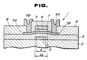
- the MOS transistor 1 has a substrate 2 which is made of quartz.
- a gate electrode 3 of polycrystalline silicon is formed on the quartz substrate 2.
- the polycrystalline silicon gate electrode 3 will be hereinafter referred to as "first gate electrode”.
- An insulation layer 4 of silicon dioxide (SiO2) is formed over the quartz substrate surface and over the polycrystalline silicon gate electrode 3.
- An active layer 5 of semiconductor layer is formed on the surface of the silicon dioxide insulation layer 4.
- the semiconductor active layer 5 is formed of polycrystalline silicon, by way of chemical vapor deposition and other appropriate process.
- the thickness of the semiconductor active layer 5 is in a range of less than or equal to 100 nm.
- the shown embodiment of the thin film MOS transistor employs polycrystalline silicon to form the semiconductor active layer
- any other material appropriate to use can be used for forming the semiconductor active layer.
- monocrystalline silicon can be used in place of the polycrystalline silicon for forming the semiconductor active layer.
- a gate insulation layer 6 and a gate electrode 7 are formed on the semiconductor active layer 5.
- the gate electrode 7 will be hereinafter referred to as "second gate electrode”.
- the gate insulation layer 6 is formed of silicon dioxide.
- the second gate electrode 7 is formed of polycrystalline silicon. These silicon dioxide gate insulation layer 6 and the second polycrystalline silicon gate electrode 7 are arranged on the semiconductor active layer 5 in alignment with the first polycrystalline silicon gate electrode 3. As will be seen from the drawing, the thickness of the silicon dioxide gate insulation layer 6 is thinner than that of the insulation layer 4. Therefore, the distance between the second polycrystalline silicon gate electrode 7 to the opposing surface of the semiconductor active layer 5 is set smaller than that between the first polycrystalline silicon gate electrode 3 and the opposing surface of the semiconductor active layer 5. As a result, the working function of the second polycrystalline silicon gate electrode 7 become greater than that of the first polycrystalline silicon gate electrode 7.
- the gate electrodes and the active layer may exhibit equivalent performance to that of the shown embodiment.
- the shown arrangement of the gate electrodes relative to the active layer is preferred because of the above discussed reasons.
- the MOS transistor 1 has an insulation layer 8 and aluminium electrodes 9A and 9B for external connection.
- the aluminium electrodes 9A and 9B are respectively connected to the source region 5A and the drain region 5B of the semiconductor active layer.
- the shown embodiment further features a novel geometry which allows easy alignment of the first and second polycrystalline silicon gate electrodes 3 and 7.
- the second polycrystalline silicon gate electrode 7 has a gate length l2.
- the first polycrystalline silicon gate electrode 3 has a gate length l1 which is shorter than the gate length l2 of the second polycrystalline silicon gate electrode 7.
- the semiconductor active layer 5 is formed in self-alignment with the first polycrystalline silicon gate electrode 7. Therefore, even when the first and second polycrystalline silicon gate electrodes 3 and 7 mutually offset to off center the each other, the first polycrystalline silicon gate electrode can be maintained beneath the second polycrystalline silicon gate electrode and beneath the region (channel region) between the source and drain regions 5A and 5B of the semiconductor active layer 5.
Landscapes
- Thin Film Transistor (AREA)
Claims (2)
- Dünnfilm-MOS-Transistor (1) mit:- einer ersten Gateelektrode (3);- einer zweiten Gateelektrode (7), die der ersten Gateelektrode gegenübersteht; und- einer aktiven Halbleiterschicht (5), die zwischen der ersten und der zweiten Gateelektrode ausgebildet ist und einen Sourcebereich (5A), einen Drainbereich (5B) und einen Kanalbereich festlegt;- wobei der Kanalbereich zwischen dem Source- und dem Drainbereich festgelegt ist und der ersten Gateelektrode über eine erste isolierende Schicht (4) gegenübersteht und der zweiten Gateelektrode über eine zweite isoliereden Schicht (6) gegenübersteht;dadurch gekennzeichnet, daß- die zweite Gateelektrode nicht mit dem Sourcebereich (5A) und dem Drainbereich überlappt;- die Gatelänge (l₁) der ersten Gateelektrode (3) kürzer ist als die Gatelänge (l₂) der zweiten Gateelektrode (7); und- die aktive Halbleiterschicht (5) in Selbstausrichtung mit der zweiten Gateelektrode (7) steht.
- Dünnfilm-MOS-Transistor (1) nach Anspruch 1, dadurch gekennzeichnet, daß die zweite isolierende Schicht (6) dünner ist als die erste isolierende Schicht (4).
Applications Claiming Priority (2)
| Application Number | Priority Date | Filing Date | Title |
|---|---|---|---|
| JP62209816A JPS6453460A (en) | 1987-08-24 | 1987-08-24 | Mos transistor |
| JP209816/87 | 1987-08-24 |
Publications (3)
| Publication Number | Publication Date |
|---|---|
| EP0304824A2 EP0304824A2 (de) | 1989-03-01 |
| EP0304824A3 EP0304824A3 (en) | 1989-05-03 |
| EP0304824B1 true EP0304824B1 (de) | 1993-03-17 |
Family
ID=16579090
Family Applications (1)
| Application Number | Title | Priority Date | Filing Date |
|---|---|---|---|
| EP88113531A Expired - Lifetime EP0304824B1 (de) | 1987-08-24 | 1988-08-19 | Dünnschicht-MOS-Transistor mit zwei Gate-Elektroden, die gegenüber der halbleitenden Schicht liegen |
Country Status (5)
| Country | Link |
|---|---|
| EP (1) | EP0304824B1 (de) |
| JP (1) | JPS6453460A (de) |
| KR (1) | KR970011766B1 (de) |
| CA (1) | CA1315421C (de) |
| DE (1) | DE3879323T2 (de) |
Families Citing this family (17)
| Publication number | Priority date | Publication date | Assignee | Title |
|---|---|---|---|---|
| US4984040A (en) * | 1989-06-15 | 1991-01-08 | Xerox Corporation | High voltage thin film transistor with second gate |
| US4984041A (en) * | 1989-07-28 | 1991-01-08 | Xerox Corporation | High voltage thin film transistor with second control electrode |
| US5173753A (en) * | 1989-08-10 | 1992-12-22 | Industrial Technology Research Institute | Inverted coplanar amorphous silicon thin film transistor which provides small contact capacitance and resistance |
| JPH0824193B2 (ja) * | 1990-10-16 | 1996-03-06 | 工業技術院長 | 平板型光弁駆動用半導体装置の製造方法 |
| US5420048A (en) * | 1991-01-09 | 1995-05-30 | Canon Kabushiki Kaisha | Manufacturing method for SOI-type thin film transistor |
| JP3254007B2 (ja) | 1992-06-09 | 2002-02-04 | 株式会社半導体エネルギー研究所 | 薄膜状半導体装置およびその作製方法 |
| US5461250A (en) * | 1992-08-10 | 1995-10-24 | International Business Machines Corporation | SiGe thin film or SOI MOSFET and method for making the same |
| US5777364A (en) * | 1992-11-30 | 1998-07-07 | International Business Machines Corporation | Graded channel field effect transistor |
| JPH07302912A (ja) | 1994-04-29 | 1995-11-14 | Semiconductor Energy Lab Co Ltd | 半導体装置 |
| JP4076648B2 (ja) | 1998-12-18 | 2008-04-16 | 株式会社半導体エネルギー研究所 | 半導体装置 |
| JP4008133B2 (ja) | 1998-12-25 | 2007-11-14 | 株式会社半導体エネルギー研究所 | 半導体装置 |
| US8158980B2 (en) | 2001-04-19 | 2012-04-17 | Semiconductor Energy Laboratory Co., Ltd. | Semiconductor device having a pixel matrix circuit that includes a pixel TFT and a storage capacitor |
| US6576202B1 (en) | 2000-04-21 | 2003-06-10 | Kin-Chung Ray Chiu | Highly efficient compact capacitance coupled plasma reactor/generator and method |
| US6982460B1 (en) | 2000-07-07 | 2006-01-03 | International Business Machines Corporation | Self-aligned gate MOSFET with separate gates |
| JP4610455B2 (ja) * | 2005-09-29 | 2011-01-12 | 株式会社半導体エネルギー研究所 | 半導体装置 |
| JP2015188062A (ja) * | 2014-02-07 | 2015-10-29 | 株式会社半導体エネルギー研究所 | 半導体装置 |
| JP2019067938A (ja) * | 2017-10-02 | 2019-04-25 | シャープ株式会社 | 薄膜トランジスタ |
Family Cites Families (3)
| Publication number | Priority date | Publication date | Assignee | Title |
|---|---|---|---|---|
| US4422090A (en) * | 1979-07-25 | 1983-12-20 | Northern Telecom Limited | Thin film transistors |
| GB2064866A (en) * | 1979-11-30 | 1981-06-17 | Gen Electric Co Ltd | Field effect semiconductor device |
| JPH0750785B2 (ja) * | 1983-10-27 | 1995-05-31 | 工業技術院長 | 電界効果トランジスタにおける短チャネル効果の抑制方法 |
-
1987
- 1987-08-24 JP JP62209816A patent/JPS6453460A/ja active Pending
-
1988
- 1988-08-19 DE DE88113531T patent/DE3879323T2/de not_active Expired - Lifetime
- 1988-08-19 EP EP88113531A patent/EP0304824B1/de not_active Expired - Lifetime
- 1988-08-19 KR KR1019880010526A patent/KR970011766B1/ko not_active Expired - Lifetime
- 1988-08-23 CA CA000575400A patent/CA1315421C/en not_active Expired - Lifetime
Also Published As
| Publication number | Publication date |
|---|---|
| DE3879323D1 (de) | 1993-04-22 |
| EP0304824A3 (en) | 1989-05-03 |
| KR970011766B1 (ko) | 1997-07-15 |
| DE3879323T2 (de) | 1993-09-30 |
| JPS6453460A (en) | 1989-03-01 |
| CA1315421C (en) | 1993-03-30 |
| KR890004444A (ko) | 1989-04-22 |
| EP0304824A2 (de) | 1989-03-01 |
Similar Documents
| Publication | Publication Date | Title |
|---|---|---|
| EP0304824B1 (de) | Dünnschicht-MOS-Transistor mit zwei Gate-Elektroden, die gegenüber der halbleitenden Schicht liegen | |
| US5140391A (en) | Thin film MOS transistor having pair of gate electrodes opposing across semiconductor layer | |
| US3890632A (en) | Stabilized semiconductor devices and method of making same | |
| US5488243A (en) | SOI MOSFET with floating gate | |
| US4924279A (en) | Thin film transistor | |
| US6303412B1 (en) | Methods of forming semiconductor-on-insulator substrates and devices and structures formed thereby | |
| US5420048A (en) | Manufacturing method for SOI-type thin film transistor | |
| US6104065A (en) | Semiconductor device having an active region in a substrate with trapezoidal cross-sectional structure | |
| JPS61102782A (ja) | Dmos半導体素子製作方法 | |
| US5418392A (en) | LDD type MOS transistor | |
| JP3287038B2 (ja) | 液晶表示装置 | |
| KR20020001420A (ko) | 완전 공핍형 에스오아이 소자의 제조방법 | |
| US6033941A (en) | Method of forming a thin film transistor with asymmetrically arranged gate electrode and offset region | |
| US5376559A (en) | Method of manufacturing a lateral field effect transistor | |
| JPH01123476A (ja) | 半導体装置およびその製法 | |
| JPS6135709B2 (de) | ||
| JP3295188B2 (ja) | Soi構造mosトランジスタの製造方法 | |
| EP0571976B1 (de) | Statisches RAM mit einem Dünnschichttransistor | |
| US5859444A (en) | Semiconductor device | |
| JP2695843B2 (ja) | 半導体装置 | |
| JPH0384963A (ja) | 薄膜トランジスタ | |
| JP2586508B2 (ja) | Mosトランジスタ | |
| JPH0728043B2 (ja) | 半導体装置 | |
| JPS63193568A (ja) | 薄膜トランジスタ | |
| JP2525615B2 (ja) | トランジスタ |
Legal Events
| Date | Code | Title | Description |
|---|---|---|---|
| PUAI | Public reference made under article 153(3) epc to a published international application that has entered the european phase |
Free format text: ORIGINAL CODE: 0009012 |
|
| AK | Designated contracting states |
Kind code of ref document: A2 Designated state(s): DE FR GB NL |
|
| PUAL | Search report despatched |
Free format text: ORIGINAL CODE: 0009013 |
|
| AK | Designated contracting states |
Kind code of ref document: A3 Designated state(s): DE FR GB NL |
|
| 17P | Request for examination filed |
Effective date: 19890926 |
|
| 17Q | First examination report despatched |
Effective date: 19910528 |
|
| GRAA | (expected) grant |
Free format text: ORIGINAL CODE: 0009210 |
|
| AK | Designated contracting states |
Kind code of ref document: B1 Designated state(s): DE FR GB NL |
|
| PG25 | Lapsed in a contracting state [announced via postgrant information from national office to epo] |
Ref country code: NL Effective date: 19930317 |
|
| REF | Corresponds to: |
Ref document number: 3879323 Country of ref document: DE Date of ref document: 19930422 |
|
| ET | Fr: translation filed | ||
| NLV1 | Nl: lapsed or annulled due to failure to fulfill the requirements of art. 29p and 29m of the patents act | ||
| PLBE | No opposition filed within time limit |
Free format text: ORIGINAL CODE: 0009261 |
|
| STAA | Information on the status of an ep patent application or granted ep patent |
Free format text: STATUS: NO OPPOSITION FILED WITHIN TIME LIMIT |
|
| 26N | No opposition filed | ||
| REG | Reference to a national code |
Ref country code: GB Ref legal event code: IF02 |
|
| PGFP | Annual fee paid to national office [announced via postgrant information from national office to epo] |
Ref country code: DE Payment date: 20070816 Year of fee payment: 20 |
|
| PGFP | Annual fee paid to national office [announced via postgrant information from national office to epo] |
Ref country code: GB Payment date: 20070815 Year of fee payment: 20 |
|
| PGFP | Annual fee paid to national office [announced via postgrant information from national office to epo] |
Ref country code: FR Payment date: 20070808 Year of fee payment: 20 |
|
| REG | Reference to a national code |
Ref country code: GB Ref legal event code: PE20 Expiry date: 20080818 |
|
| PG25 | Lapsed in a contracting state [announced via postgrant information from national office to epo] |
Ref country code: GB Free format text: LAPSE BECAUSE OF EXPIRATION OF PROTECTION Effective date: 20080818 |