EP0304064A2 - Mehrstufige Koppelanordnung - Google Patents
Mehrstufige Koppelanordnung Download PDFInfo
- Publication number
- EP0304064A2 EP0304064A2 EP88113451A EP88113451A EP0304064A2 EP 0304064 A2 EP0304064 A2 EP 0304064A2 EP 88113451 A EP88113451 A EP 88113451A EP 88113451 A EP88113451 A EP 88113451A EP 0304064 A2 EP0304064 A2 EP 0304064A2
- Authority
- EP
- European Patent Office
- Prior art keywords
- binary
- optical
- couplers
- coupler
- switching
- Prior art date
- Legal status (The legal status is an assumption and is not a legal conclusion. Google has not performed a legal analysis and makes no representation as to the accuracy of the status listed.)
- Granted
Links
Images
Classifications
-
- H—ELECTRICITY
- H04—ELECTRIC COMMUNICATION TECHNIQUE
- H04Q—SELECTING
- H04Q11/00—Selecting arrangements for multiplex systems
- H04Q11/0001—Selecting arrangements for multiplex systems using optical switching
- H04Q11/0005—Switch and router aspects
-
- H—ELECTRICITY
- H04—ELECTRIC COMMUNICATION TECHNIQUE
- H04Q—SELECTING
- H04Q11/00—Selecting arrangements for multiplex systems
- H04Q11/0001—Selecting arrangements for multiplex systems using optical switching
- H04Q11/0005—Switch and router aspects
- H04Q2011/0052—Interconnection of switches
Definitions
- LWL fiber optic
- two strip waveguides - are narrow thin strips produced by diffusion (e.g. of titanium in lithium niobate) in a substrate and have a larger optical refractive index than the substrate - are very narrow in a coupling area of a certain length, at a distance of typically about 5 ⁇ m, guided side by side so that the optical fields overlap and light energy can be coupled from one strip waveguide to the other strip waveguide;
- 2x2 coupling elements which are only capable of two switching states - namely uncrossed switching and crossed switching - are also referred to as binary couplers in switching technology (DE-PS 2 036 176), controllable electro-optical directional couplers used as 2x2 coupling elements can also be used as optical binary couplers be addressed.
- the object of the invention is to provide a switching network in which, in such a case, no switching network connection is nevertheless connected to another switching network connection.
- the invention relates to a multi-stage coupling arrangement with a plurality of optical binary couplers interconnected symmetrically to the switching center line;
- This coupling arrangement is characterized according to the invention in that each switching matrix connection forms the tip of an individual pyramid of optical binary couplers, each pyramid ending in front of the switching center line, in which each optical binary coupler on the side facing away from the switching center line is unconnected in one of its two optical paths and that is via the switching center is connected to each other on the other side of the binary coupler pyramid in a light-conducting manner such that each switching matrix interconnection path starting from a switching matrix connection or leading to a switching matrix connection contains such an unconnected optical fiber path of an optical binary coupler when all binary couplers are switched through.
- the invention has the advantage of being able to avoid undesired connections of switching matrix connections in a coupling arrangement formed with optical binary couplers in the event of failure of the binary coupler control voltages.
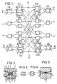
- FIG. 1 shows schematically, in a scope necessary for understanding the invention, an exemplary embodiment of a multi-stage coupling arrangement according to the invention, which is connected to a plurality of optical binary couplers IIA,..., INA; IlJl, ..., INJn; lJlO, ..., nJNO; AlO, ..., ANO is formed; these binary couplers are grouped into switching matrix connection-specific pyramids, the apex of which is formed by the respective switching matrix connection and the base of which lies in front of the switching matrix center line M - M.
- Optical binary couplers are known per se, for example in the form of controllable electro-optical directional couplers (e.g. from the literature references mentioned at the beginning); they are each capable of only two switching states, namely the state of an uncrossed connection, as indicated in FIG. 3, and the state of a crossed connection, as indicated in FIG. 4. 2 schematically shows such an optical binary coupler formed with a controllable electro-optical directional coupler in essential details:
- Two strip waveguides a ′ - i ′ and a ⁇ - i ⁇ are diffused into a substrate, for example lithium niobate; In the actual coupling area having a certain length, the two strip waveguides are closely guided at a distance of typically about 5 ⁇ m, so that light energy can be coupled from one to the other strip waveguide.
- control electrodes E, E ', E ⁇ and O, O', O ⁇ which can be acted upon by a corresponding electrical control voltage from control signal terminals s, so that no overcoupling takes place; the binary coupler is then in the uncrossed state in which, for example, light entering the light guide path a ⁇ exits the light guide path i ⁇ again.
- the state of a cross-connection in which, for example, light entering the light guide path a ⁇ emerges again from the light guide path i ′, there is such an optical binary coupler in the absence of a control voltage, for example due to a supply voltage failure. Accordingly, in order to return to FIG.
- the switching network connection IN is optically connected to the switching network connection 10, and it is, for example, at uncrossed connection of the two binary couplers IlA and 1JNO and crossed connection of the two binary couplers IlJn and ANO the switching network connection Il with the switching network connection NO is connected in a light-conducting manner.
- each optical binary coupler of the individual switching network connection individual pyramids of optical binary couplers on the side applied to the switching network center line M - M is not connected in one of its two light guide paths; Over the switching center line M - M, the binary coupler pyramids are connected in a light-conducting manner to each binary coupler pyramid lying on the other side such that each switching matrix interconnection path starting from a switching matrix connection or leading to a switching matrix connection, with all binary couplers crossed through, connects such an unconnected optical conductor path of an optical binary coupler contains.
- the coupling arrangement sketched in FIG. 1 is a 4-stage 4x4 coupling arrangement with 2-stage coupling field connection-specific binary coupler pyramids.
- the invention is not limited to the realization of the binary couplers with controllable optoelectric directional couplers, which is illustrated in FIG. 2; Rather, the binary couplers can also be implemented differently, for example with so-called Bragg reflectors, as is indicated schematically in FIG. 5:
- an electro-optical crystal for example lithium niobate
- diffusion for example of titanium
- two are under twice the so-called Bragg-Winkel intersecting strip waveguides a '- i ⁇ and a ⁇ - i' are formed, in the intersection of which a finger-shaped electrode structure is provided, which can be acted upon by a corresponding electrical control voltage from control signal terminals s.
- a refractive index grating can be generated in the intersection area due to the electro-optical effect, on which light incident at the Bragg angle is deflected, so that incident light and deflected light enclose the double Bragg angle (see, for example, DE-A 3 025 083, FIG. 1):
- the binary coupler according to FIG. 5 is then in the uncrossed state in which, for example, light entering the light guide path a ⁇ exits the light guide path i ⁇ again.
- the binary coupler is then in the state of crossed connection, in which, for example, light entering the light guide path a ⁇ emerges again from the light guide path i '.
- the unconnected light guide path of the optical binary coupler denoted by a in FIG. 5 can in turn be terminated with a light-absorbing layer Z.
Landscapes
- Engineering & Computer Science (AREA)
- Computer Networks & Wireless Communication (AREA)
- Use Of Switch Circuits For Exchanges And Methods Of Control Of Multiplex Exchanges (AREA)
- Optical Communication System (AREA)
- Optical Integrated Circuits (AREA)
- Oscillators With Electromechanical Resonators (AREA)
- Data Exchanges In Wide-Area Networks (AREA)
- Small-Scale Networks (AREA)
Abstract
Description
- Neuere Entwicklungen der Fernmeldetechnik führen zu Lichtwellenleiter-(LWL-)Kommunikationssystemen, in denen nicht nur die zwischen Vermittlungsstelle und Teilnehmerstellen verlaufenden Teilnehmeranschlußleitungen durch Lichtwellenleiter gebildet sind (DE-PS 24 21 002), sondern in denen auch die Verbindungsdurchschaltung in der Vermittlungsstelle mit Hilfe von lichtleitenden IO-(Integrierte-Optik-)2x2-Schaltelementen z.B. in Form von steuerbaren elektrooptischen Richtkopplern bewirkt werden kann (ISS'84 Conference Papers 41A4, Fig. 3, 5, 6 und 8; 1986 International Zürich Seminar Conf. Papers C7, Fig.1, 2, 4).
- Bei einem steuerbaren elektrooptischen Richtkoppler sind zwei Streifenwellenleiter - das sind durch Eindiffusion (z.B. von Titan in Lithiumniobat) in einem Substrat erzeugte schmale dünne Streifen, die eine größere optische Brechzahl als das Substrat haben, - in einem Koppelbereich bestimmter Länge sehr eng, in einem Abstand von typischerweise etwa 5µm, nebeneinander geführt, so daß sich die optischen Felder überlappen und Lichtenergie von dem einen Streifenwellenleiter auf den anderen Streifenwellenleiter übergekoppelt werden kann; im Koppelbereich neben und zwischen den Streifenwellenleitern befinden sich Steuerelektroden, die mit einem die Überkopplung beeinflussenden elektrischen Steuersignal beaufschlagt sind: Bei Anliegen einer entsprechenden Steuerspannung findet keine Überkopplung statt; das Fehlen einer Steuerspannung kann mit einer vollständigen Überkopplung verbunden sein (ntz 39(1986)12, 828...830, Bild 3c und 3d; telcom report 10(1987)2, 90...98, Bild 8).
- Nachdem in der Vermittlungstechnik 2x2-Koppelelemente, die nur zweier Schaltzustände - nämlich ungekreuzte Durchschaltung und gekreuzte Durchschaltung - fähig sind, auch als Binärkoppler bezeichnet werden (DE-PS 2 036 176), können als 2x2-Koppelelemente eingesetzte steuerbare elektrooptische Richtkoppler auch als optische Binärkoppler angesprochen werden.
- Mit Binärkopplern können auch grössere Koppelanordnungen gebildet werden (DE-PS 2 036 176; ISS'84 Conf. Papers a.a.O.; 1986 Intern. Zürich Seminar Conf. Papers a.a.O); mit wenigstens fünf in drei Stufen angeordneten, auf einem IO-(Integrierte-Optik-)Baustein enthaltenen optischen Binärkopplern lässt sich z.B. eine optische 4x4-Koppelanordnung realisieren (ElectronicsWeek March 18, 1985, 55...58, Fig. 7).
- Daß bei mit Binärkopplern gebildeten Koppelanordnungen die einzelnen Binärkoppler sich jeweils stets in dem einen oder in dem anderen Durchschaltezustand befinden, - einer mit optischen Binärkopplern gebildeten Koppelanordnung sind bei einem z.B. durch den Ausfall der Versorgungsspannung bedingten Fehlen aller Steuerspannungen alle Binärkoppler im Zustand der gekreuzten Durchschaltung, - macht ggf. die Vermeidung unerwünschter Verbindungen zu einem Problem.
- Die Erfindung stellt sich nun die Aufgabe, eine Koppelanordnung anzugeben, in der in einem solchen Fall dennoch kein Koppelfeldanschluß mit einem anderen Koppelfeldanschluß verbunden ist.
- Die Erfindung betrifft eine mehrstufige Koppelanordnung mit einer Mehrzahl von symmetrisch zur Koppelfeldmittellinie miteinander verbundenen optischen Binärkopplern; diese Koppelanordnung ist erfindungsgemäß dadurch gekennzeichnet, daß jeder Koppelfeldanschluß die Spitze einer koppelfeldanschlußindividuellen, jeweils vor der Koppelfeldmittellinie endenden Pyramide von optischen Binärkopplern bildet, in der jeder optische Binärkoppler auf der der Koppelfeldmittellinie abgewandten Seite in dem einen seiner beiden Lichtleitpfade unbeschaltet ist und die über die Koppelfeldmittellinie hinweg mit jeder auf deren anderer Seite liegenden Binärkopplerpyramide derart lichtleitend verbunden ist, daß jeder von einem Koppelfeldanschluß ausgehende bzw. zu einem Koppelfeldanschluß hinführende Koppelfelddurchschaltepfad bei gekreuzter Durchschaltung aller Binärkoppler einen solchen unbeschalteten Lichtleiterpfad eines optischen Binärkopplers enthält.
- Es sei an dieser Stelle bemerkt, daß (z.B. aus DE-PS 582 206 oder aus DE-PS 1 115 775) Relais-Umschaltkontakt-Pyramiden und (z.B. aus EP-A-O 146 275) auch andere mit einfachen Umschaltern gebildete Koppelfeldstrukturen bekannt sind. Probleme einer Vermeidung unerwünschter Verbindungen bei Spannungsausfall in einer mit optischen Binärkopplern gebildeten Koppelanordnung bleiben dabei unberührt; hierzu zeigt aber die Erfindung einen Weg.
- Die Erfindung bringt den Vorteil mit sich, in einer mit optischen Binärkopplern gebildeten Koppelanordnung unerwünschte Verbindungen von Koppelfeldanschlüssen bei Ausfall der Binärkoppler-Steuerspannungen vermeiden zu können.
- Weitere Besonderheiten der Erfindung werden aus der nachfolgenden näheren Erläuterung eines Ausführungsbeispiels anhand der Zeichnung ersichtlich. Dabei zeigt
- FIG 1 ein Ausführungsbeispiel einer Koppelanordnung gemäß der Erfindung;
- FIG 2 und FIG 5 zeigen jeweils schematisch einen darin enthaltenen optischen Binärkoppler in Form eines steuerbaren elektrooptischen Richtkopplers bzw. eines Bragg-Reflektors.
- FIG 3 und FIG 4 verdeutlichen die beiden Durchschaltzustände solcher Binärkoppler.
- In FIG 1 ist schematisch in einem zum Verständnis der Erfindung erforderlichen Umfange ein Ausführungsbeispiel einer mehrstufigen Koppelanordnung gemäß der Erfindung dargestellt, die mit einer Mehrzahl von symmetrisch zu einer Koppelfeldmittellinie M - M stufenweise miteinander verbundenen optischen Binärkopplern IlA, ...,INA; IlJl,...,INJn; lJlO,...,nJNO; AlO,...,ANO gebildet ist; diese Binärkoppler sind zu koppelfeldanschlußindividuellen Pyramiden gruppiert, deren Spitze vom jeweiligen Koppelfeldanschluß gebildet wird und deren Basis jeweils vor der Koppelfeldmittellinie M - M liegt.
- Optische Binärkoppler sind beispielsweise in Form von steuerbaren elektrooptischen Richtkopplern an sich (z.B. aus den dazu eingangs genannten Literaturstellen) bekannt; sie sind jeweils nur zweier Schaltzustände fähig, nämlich des Zustands einer ungekreuzten Durchschaltung, wie dies in FIG 3 angedeutet ist, und des Zustands einer gekreuzten Durchschaltung, wie dies in FIG 4 angedeutet ist. FIG 2 zeigt schematisch einen solchen mit einem steuerbaren elektrooptischen Richtkoppler gebildeten optischen Binärkoppler in wesentlichen Einzelheiten:
- In ein Substrat, z.B. Lithiumniobat, sind zwei Streifenwellenleiter a′ - i′ und a˝ - i˝ eindiffundiert; in dem eine bestimmte Länge aufweisenden eigentlichen Koppelbereich sind die beiden Streifenwellenleiter eng, in einem Abstand von typischerweise etwa 5 µm, nebeneinander geführt, so daß Lichtenergie vom jeweils einen auf den jeweils anderen Streifenwellenleiter übergekoppelt werden kann. Im Koppelbereich befinden sich Steuerelektroden E, E′, E˝ und O, O′, O˝, die von Steuersignalklemmen s her mit einer entsprechenden elektrischen Steuerspannung beaufschlagt sein können, so daß keine Überkopplung stattfindet; der Binärkoppler befindet sich dann im Zustand der ungekreuzten Durchschaltung, in dem z.B. in den Lichtleiterpfad a˝ eintretendes Licht aus dem Lichtleiterpfad i˝ wieder austritt. Im Zustand einer gekreuzten Durchschaltung, in dem z.B. in den Lichtleiterpfad a˝ eintretendes Licht aus dem Lichtleiterpfad i′ wieder austritt, befindet sich ein solcher optischer Binärkoppler bei - etwa durch einen Versorgungsspannungsausfall bedingt - fehlender Steuerspannung. Dementsprechend ist dann, um wieder auf FIG 1 zurückzukommen, in der dort skizierten Koppelanordnung beispielsweise bei ungekreuzter Durchschaltung der zwei Binärkoppler INA und nJlO und Gekreuzter Durchschaltung der zwei Binärkoppler INJl und AlO der Koppelfeldanschluß IN mit dem Koppelfeldanschluß lO lichtleitend verbunden, und es ist beispielsweise bei ungekreuzter Durchschaltung der beiden Binärkoppler IlA and 1JNO und gekreuzter Durchschaltung der beiden Binärkoppler IlJn und ANO der Koppelfeldanschluß Il mit dem Koppelfeldanschluß NO lichtleitend verbunden.
- Bei einem z.B. durch einen Versorgungsspannungsausfall bedingten Fehlen aller Steuerspannungen befinden sich alle Binärkoppler der in FIG 1 skizzierten Koppelanordnung im Zustand der gekreuzten Durchschaltung. Um nun sicherzustellen, daß dabei dennoch kein Koppelfeldanschluß mit einem anderen Koppelfeldanschluß verbunden ist, ist jeder optische Binärkoppler der einzelnen koppelfeldanschlußindividuellen Pyramiden von optischen Binärkopplern auf der der Koppelfeldmittellinie M - M angewandten Seite in dem einen seiner beiden Lichtleitpfade unbeschaltet; über Koppelfeldmittellinie M - M hinweg sind die Binärkoppler-Pyramiden mit jeder auf der anderen Seite liegenden Binärkoppler-Pyramide derart lichtleitend verbunden, daß jeder von einem Koppelfeldanschluß ausgehende bzw. zu einem Koppelfeldanschluß hinführende Koppelfelddurchschaltepfad bei gekreuzter Durchschaltung aller Binärkoppler einen solchen unbeschalteten Lichtleiterpfad eines optischen Binärkopplers enthält. In FIG 1 und ebenso in FIG 2 ist der jeweils unbeschaltete Lichtleiterpfad eines optischen Binärkopplers jeweils mit a′ bezeichnet. Um störende Reflektionen in einem solchen unbeschalteten Lichtleiterpfad a′ zu vermeiden, kann dieser zweckmäßigerweise mit einem Lichtabsorber abgeschlossen sein, der auf ihn vom Lichtleiterpfad a′ her auftreffendes Licht völlig absorbiert; in FIG 2 ist eine solche lichtabsorbierende Schicht mit Z bezeichnet.
- Kommt es nun zu einem Spannungsausfall, aufgrund dessen sämtliche optische Binärkoppler in den Zustand gekreuzter Durchschaltung gelangen, so wird in der in FIG 1 skizzierten Koppelanordnung beispielsweise eine vom Koppelfeldenanschluß Il ausgehende Verbindung über die jeweils gekreuzt durchschaltenden Binärkoppler IlA, IlJl und lJlO zum unbeschalteten Lichtleiterpfad a′ des Binärkopplers lJlO geführt und endet dort; in ähnlicher Weise sind auch alle übrigen Koppelfeldanschlüsse ...,IN; lO, ...,NO über zwei oder drei jeweils gekreuzt durchschaltende optische Binärkoppler mit einem umbeschalteten Lichtleiterpfad a′ eines solchen Binärkopplers verbunden, ohne daß dies hier jeweils einzeln erläutert werden werden muß.
- Bei der in FIG 1 skizzierten Koppelanordnung handelt es sich um eine 4-stufige 4x4-Koppelanordnung mit 2-stufigen koppelfeldanschlußindividuellen Binärkopplerpyramiden. Die Erfindung ist indessen auf eine solche Konfiguration nicht beschränkt; sie kann vielmehr ganz allgemein in 2n-stufigen NxN-Koppelanordnungen mit n-stufigen koppelfeldanschlußindividuellen Binärkopplerpyramiden (mit n = 1b N) Anwendung finden.
- Ebenso ist die Erfindung nicht auf die in FIG 2 verdeutlichte Realisierung der Binärkoppler mit steuerbaren optoelektrischen Richtkopplern beschränkt; die Binärkoppler können vielmehr auch anders realisiert sein, etwa mit sog. Bragg-Reflektoren, wie dies in FIG 5 schematisch angedeutet ist: Hier sind in einen elektrooptischen Kristall, z.B. Lithiumniobat, durch Eindiffusion (z.B. von Titan) zwei sich unter dem Doppelten des sog. Bragg-Winkels kreuzende Streifenwellenleiter a′ - i˝ und a˝ - i′ gebildet, in deren Kreuzungsbereich eine fingerförmige Elektrodenstruktur vorgesehen ist, die von Steuersignalklemmen s her mit einer entsprechenden elektrischen Steuerspannung beaufschlagbar sind. Durch eine solche Steuerspannung kann auf Grund des elektrooptischen Effekts im Kreuzungsbereich ein Brechzahlgitter erzeugt werden, an dem unter dem Bragg-Winkel auftreffendes Licht abgelenkt wird, so daß auftreffendes Licht und abgelenktes Licht den doppelten Bragg-Winkel einschliessen (vgl. z.B. DE-A-3 025 083, FIG 1): Der Binärkoppler gemäß FIG 5 befindet sich dann im Zustand der ungekreuzten Durchschaltung, in dem z.B. in den Lichtleiterpfad a˝ eintretendes Licht aus dem Lichtleiterpfad i˝ wieder austritt.
Bei fehlender Steuerspannung kommt es nicht zu einer solchen Ablenkung des Lichts; der Binärkoppler befindet sich dann im Zustand der gekreuzten Durchschaltung, in dem z.B. in den Lichtleiterpfad a˝ eintretendes Licht aus dem Lichtleiterpfad i′ wieder austritt.
Der in FIG 5 mit a′ bezeichnete unbeschaltete Lichtleiterpfad des optischen Binärkopplers kann wiederum mit einer lichtabsorbierenden Schicht Z abgeschlossen sein.
Claims (2)
dadurch gekennzeichnet,
daß jeder Koppelfeldanschluß (Ilm ..., IN; lO, ..., NO) die Spitze einer koppelfeldanschlußindividuellen, jeweils vor der Koppelfeldmittellinie (M - M) endenden Pyramide von optischen Binärkopplern (IAl, IlJl, IlJn, ..., nJNO, lJNO, ANO) bildet,
in der jeder optische Binärkoppler (IAl, IlJl, IlJn; ...; nJNO, lJNO, ANO) auf der der Koppelfeldmittellinie (M - M) abgewandten Seite in dem einen seiner beiden Lichtleitpfade (a′) unbeschaltet ist
und die über die Koppelfeldmittellinie (M - M) hinweg mit jeder auf deren anderer Seite liegenden Binärkopplerpyramide (lJ10 nJ10, A10; ...; lJNO, nJNO, ANO; IlJ1, IlJn, IlA; ...; INJl, INJn, INA) derart lichtleitend verbunden ist, daß jeder von einem Koppelfeldanschluß (Il, ..., IN) ausgehende bzw. zu einem Koppelfeldanschluß (lO, ..., NO) hinführende Koppelfelddurchschaltepfad bei gekreuzter Durchschaltung aller Binärkoppler (IlA, ..., ANO) einen solchen unbeschalteten Lichtleiterpfad (a′) eines optischen Binärkopplers enthält.
dadurch gekennzeichnet,
daß der unbeschaltete Lichtleiterpfad (a′) mit einem Lichtabsorber (Z) abgeschlossen ist.
Priority Applications (1)
| Application Number | Priority Date | Filing Date | Title |
|---|---|---|---|
| AT88113451T ATE96598T1 (de) | 1987-08-20 | 1988-08-18 | Mehrstufige koppelanordnung. |
Applications Claiming Priority (2)
| Application Number | Priority Date | Filing Date | Title |
|---|---|---|---|
| DE3727827 | 1987-08-20 | ||
| DE3727827 | 1987-08-20 |
Publications (3)
| Publication Number | Publication Date |
|---|---|
| EP0304064A2 true EP0304064A2 (de) | 1989-02-22 |
| EP0304064A3 EP0304064A3 (en) | 1990-07-04 |
| EP0304064B1 EP0304064B1 (de) | 1993-10-27 |
Family
ID=6334147
Family Applications (1)
| Application Number | Title | Priority Date | Filing Date |
|---|---|---|---|
| EP88113451A Expired - Lifetime EP0304064B1 (de) | 1987-08-20 | 1988-08-18 | Mehrstufige Koppelanordnung |
Country Status (9)
| Country | Link |
|---|---|
| US (1) | US5010542A (de) |
| EP (1) | EP0304064B1 (de) |
| JP (1) | JPS6490423A (de) |
| AT (1) | ATE96598T1 (de) |
| CA (1) | CA1311384C (de) |
| DE (1) | DE3885198D1 (de) |
| HU (1) | HU200051B (de) |
| LU (1) | LU87165A1 (de) |
| RU (1) | RU1776358C (de) |
Families Citing this family (13)
| Publication number | Priority date | Publication date | Assignee | Title |
|---|---|---|---|---|
| GB8904281D0 (en) * | 1989-02-24 | 1989-04-12 | British Telecomm | Optical interconnect networks |
| GB8925454D0 (en) * | 1989-11-10 | 1989-12-28 | British Telecomm | Generalised connection network |
| US5311345A (en) * | 1992-09-30 | 1994-05-10 | At&T Bell Laboratories | Free space optical, growable packet switching arrangement |
| JPH07312576A (ja) * | 1994-05-17 | 1995-11-28 | Sumitomo Electric Ind Ltd | 光伝送路の故障検出方式 |
| US5524154A (en) * | 1994-08-31 | 1996-06-04 | At&T Corp. | Hybrid architecture for an optical switching fabric implemented with 1×2 switching devices |
| DE4437325A1 (de) * | 1994-10-19 | 1996-04-25 | Bosch Gmbh Robert | Optischer Schalter und optisches Koppelfeld damit |
| KR0159663B1 (ko) * | 1995-10-28 | 1998-12-01 | 김광호 | 광데이타 전송 이중화를 구현한 광데이타 전송장치 |
| US6236775B1 (en) * | 1998-05-19 | 2001-05-22 | Lynx Photonic Networks Inc. | Integrated optical switch array |
| US6445843B1 (en) * | 2000-12-20 | 2002-09-03 | Lynx Photonic Networks Inc. | Optical switching system with power balancing |
| CA2404473A1 (en) * | 2000-03-27 | 2001-10-04 | Lynx Photonic Networks, Inc. | Optical switching system with power balancing |
| JP2003199130A (ja) * | 2001-12-27 | 2003-07-11 | Fujitsu Ltd | 光パスクロスコネクト装置及びその切替方法 |
| US8351338B2 (en) * | 2009-03-23 | 2013-01-08 | Jds Uniphase Corporation | Sharing single tester among plurality of active communication links |
| CN103370650B (zh) * | 2011-02-15 | 2016-01-06 | 日本电信电话株式会社 | 波导型光开关 |
Family Cites Families (15)
| Publication number | Priority date | Publication date | Assignee | Title |
|---|---|---|---|---|
| DE582206C (de) * | 1929-01-09 | 1933-08-10 | Siemens & Halske Akt Ges | Schaltungsanordnung fuer Relaiswaehler |
| DE1115775B (de) * | 1960-03-08 | 1961-10-26 | Siemens Ag | Relaiskontaktpyramide fuer Fernmelde-, insbesondere Fernsprechanlagen |
| AT318018B (de) * | 1970-07-21 | 1974-09-25 | Siemens Ag | Koppelanordnung mit einer Mehrzahl von untereinander verbundenen, jeweils nur zwei erste und zwei zweite Leitungen aufweisenden Koppelvielfachen (Binärkopplern) |
| DE2421002C3 (de) * | 1974-04-30 | 1980-07-03 | Siemens Ag, 1000 Berlin Und 8000 Muenchen | Nachrichtenvermittlungssystem |
| US4011543A (en) * | 1976-02-20 | 1977-03-08 | Sperry Rand Corporation | Low crosstalk optical switch |
| DE3025083A1 (de) * | 1980-07-02 | 1982-01-21 | Siemens AG, 1000 Berlin und 8000 München | Planarer elektrooptischer lichtablenker fuer mehrere strahlpositionen |
| DE3230251A1 (de) * | 1981-09-30 | 1984-01-05 | Siemens AG, 1000 Berlin und 8000 München | Als schalter dienender richtungskoppler fuer optische signale und verfahren zur herstellung desselben |
| DE3235266A1 (de) * | 1982-09-23 | 1984-03-29 | Siemens AG, 1000 Berlin und 8000 München | Kopplernetzwerk zum verkoppeln mehrerer teilnehmersender mit mehreren teilnehmerempfaengern |
| GB8333519D0 (en) * | 1983-12-16 | 1984-01-25 | Gen Electric Co Plc | Data signal switching systems |
| DE3423221A1 (de) * | 1984-06-21 | 1984-11-29 | Heinrich-Hertz-Institut für Nachrichtentechnik Berlin GmbH, 1000 Berlin | Optischer sternkoppler mit einer grossen zahl von ein- und ausgaengen |
| SE450173B (sv) * | 1985-08-15 | 1987-06-09 | Ericsson Telefon Ab L M | Polarisationsoberoende elektrooptisk omkopplare |
| US4731878A (en) * | 1985-11-29 | 1988-03-15 | American Telephone And Telegraph Company, At&T Bell Laboratories | Self-routing switch node combining electronic and photonic switching |
| CA1284904C (en) * | 1986-01-31 | 1991-06-18 | Kazuo Hajikano | Optical space switch |
| US4787692A (en) * | 1987-03-13 | 1988-11-29 | American Telephone And Telegraph Company At&T Bell Laboratories | Electro optical switch architectures |
| US4807280A (en) * | 1987-09-18 | 1989-02-21 | Pacific Bell | Cross-connect switch |
-
1988
- 1988-03-16 LU LU87165A patent/LU87165A1/de unknown
- 1988-07-29 RU SU884356166A patent/RU1776358C/ru active
- 1988-08-15 US US07/232,504 patent/US5010542A/en not_active Expired - Fee Related
- 1988-08-15 JP JP63203689A patent/JPS6490423A/ja active Pending
- 1988-08-18 DE DE88113451T patent/DE3885198D1/de not_active Expired - Fee Related
- 1988-08-18 CA CA000575087A patent/CA1311384C/en not_active Expired - Lifetime
- 1988-08-18 EP EP88113451A patent/EP0304064B1/de not_active Expired - Lifetime
- 1988-08-18 AT AT88113451T patent/ATE96598T1/de active
- 1988-08-19 HU HU884410A patent/HU200051B/hu not_active IP Right Cessation
Also Published As
| Publication number | Publication date |
|---|---|
| JPS6490423A (en) | 1989-04-06 |
| ATE96598T1 (de) | 1993-11-15 |
| EP0304064B1 (de) | 1993-10-27 |
| DE3885198D1 (de) | 1993-12-02 |
| EP0304064A3 (en) | 1990-07-04 |
| RU1776358C (ru) | 1992-11-15 |
| CA1311384C (en) | 1992-12-15 |
| HUT47772A (en) | 1989-03-28 |
| US5010542A (en) | 1991-04-23 |
| LU87165A1 (de) | 1988-08-23 |
| HU200051B (en) | 1990-03-28 |
Similar Documents
| Publication | Publication Date | Title |
|---|---|---|
| DE3876434T2 (de) | Verbesserungen in elektro-optischen schalterarchitekturen. | |
| EP0304064B1 (de) | Mehrstufige Koppelanordnung | |
| DE3124488C2 (de) | Elektrooptischer Schalter mit Flüssigkristallmatrixzelle | |
| DE69529626T2 (de) | Optischer wellenleiterkreuzungspunktschalter | |
| DE2400491C2 (de) | Fasernetz für die optoelektronische Übertragung von Daten | |
| DE69927636T2 (de) | Multiport optischer Zirkulator welcher eine Abbildungslinse und ein korrigierendes optisches Element benutzt | |
| DE60023048T2 (de) | Optische Raumkoppelfelder mit Mehrtor-Kopplern | |
| WO1996008932A1 (de) | Optische 1xn- und nxn-schaltmatrix in baumstruktur | |
| EP0968452B1 (de) | Optisches schaltelement und schaltanordnung | |
| EP0053324B1 (de) | Optisches Verzweigungsglied | |
| DE69901650T2 (de) | Optischer Mehrfachkoppler mit Linse | |
| DE3644309A1 (de) | Integrierter optischer schalter | |
| EP0419720B1 (de) | Lichtwellenleiter-Telekommunikationssystem mit einem oder mehreren im LWL-Weg liegenden optischen Schalter(n) | |
| DE60101369T2 (de) | Optische Schaltmatrix | |
| EP0587930B1 (de) | Verfahren zur Durchschaltung von optischen Nachrichtenzellen | |
| EP0807357B1 (de) | VERFAHREN ZUM BETRIEB EINER MEHRSTUFIGEN NxN-RAUMKOPPELANORDNUNG | |
| EP0968454A1 (de) | Optischer mehrfachschalter | |
| LU87901A1 (de) | Passives optisches telekommunikationssystem | |
| DE60127667T2 (de) | Optischer flüssigkristallschalter mit zuverlässiger steuerung | |
| DE102007015766A1 (de) | Lasermodul für Projektoren | |
| DD152212A1 (de) | Optisches system zur umwandlung der polarisation von licht | |
| EP0304065A1 (de) | Telekommunikationssystem mit einem Sternnetz von LWL-Anschlussleitungen | |
| DE3423221A1 (de) | Optischer sternkoppler mit einer grossen zahl von ein- und ausgaengen | |
| EP1337900B1 (de) | Schaltungsanordnung | |
| DE3218193A1 (de) | Opto-elektronische schaltmatrix |
Legal Events
| Date | Code | Title | Description |
|---|---|---|---|
| PUAI | Public reference made under article 153(3) epc to a published international application that has entered the european phase |
Free format text: ORIGINAL CODE: 0009012 |
|
| AK | Designated contracting states |
Kind code of ref document: A2 Designated state(s): AT BE CH DE FR GB IT LI NL SE |
|
| PUAL | Search report despatched |
Free format text: ORIGINAL CODE: 0009013 |
|
| AK | Designated contracting states |
Kind code of ref document: A3 Designated state(s): AT BE CH DE FR GB IT LI NL SE |
|
| 17P | Request for examination filed |
Effective date: 19901220 |
|
| 17Q | First examination report despatched |
Effective date: 19921216 |
|
| GRAA | (expected) grant |
Free format text: ORIGINAL CODE: 0009210 |
|
| AK | Designated contracting states |
Kind code of ref document: B1 Designated state(s): AT BE CH DE FR GB IT LI NL SE |
|
| REF | Corresponds to: |
Ref document number: 96598 Country of ref document: AT Date of ref document: 19931115 Kind code of ref document: T |
|
| REF | Corresponds to: |
Ref document number: 3885198 Country of ref document: DE Date of ref document: 19931202 |
|
| ITF | It: translation for a ep patent filed | ||
| GBT | Gb: translation of ep patent filed (gb section 77(6)(a)/1977) |
Effective date: 19940107 |
|
| ET | Fr: translation filed | ||
| PLBE | No opposition filed within time limit |
Free format text: ORIGINAL CODE: 0009261 |
|
| STAA | Information on the status of an ep patent application or granted ep patent |
Free format text: STATUS: NO OPPOSITION FILED WITHIN TIME LIMIT |
|
| 26N | No opposition filed | ||
| EAL | Se: european patent in force in sweden |
Ref document number: 88113451.4 |
|
| PGFP | Annual fee paid to national office [announced via postgrant information from national office to epo] |
Ref country code: GB Payment date: 19960718 Year of fee payment: 9 |
|
| PGFP | Annual fee paid to national office [announced via postgrant information from national office to epo] |
Ref country code: AT Payment date: 19960724 Year of fee payment: 9 |
|
| PGFP | Annual fee paid to national office [announced via postgrant information from national office to epo] |
Ref country code: BE Payment date: 19960819 Year of fee payment: 9 |
|
| PGFP | Annual fee paid to national office [announced via postgrant information from national office to epo] |
Ref country code: SE Payment date: 19960821 Year of fee payment: 9 Ref country code: NL Payment date: 19960821 Year of fee payment: 9 |
|
| PGFP | Annual fee paid to national office [announced via postgrant information from national office to epo] |
Ref country code: FR Payment date: 19960830 Year of fee payment: 9 |
|
| PGFP | Annual fee paid to national office [announced via postgrant information from national office to epo] |
Ref country code: DE Payment date: 19961022 Year of fee payment: 9 |
|
| PGFP | Annual fee paid to national office [announced via postgrant information from national office to epo] |
Ref country code: CH Payment date: 19961114 Year of fee payment: 9 |
|
| PG25 | Lapsed in a contracting state [announced via postgrant information from national office to epo] |
Ref country code: GB Free format text: LAPSE BECAUSE OF NON-PAYMENT OF DUE FEES Effective date: 19970818 Ref country code: AT Free format text: LAPSE BECAUSE OF NON-PAYMENT OF DUE FEES Effective date: 19970818 |
|
| PG25 | Lapsed in a contracting state [announced via postgrant information from national office to epo] |
Ref country code: SE Free format text: LAPSE BECAUSE OF NON-PAYMENT OF DUE FEES Effective date: 19970819 |
|
| PG25 | Lapsed in a contracting state [announced via postgrant information from national office to epo] |
Ref country code: LI Free format text: LAPSE BECAUSE OF NON-PAYMENT OF DUE FEES Effective date: 19970831 Ref country code: CH Free format text: LAPSE BECAUSE OF NON-PAYMENT OF DUE FEES Effective date: 19970831 Ref country code: BE Free format text: LAPSE BECAUSE OF NON-PAYMENT OF DUE FEES Effective date: 19970831 |
|
| BERE | Be: lapsed |
Owner name: SIEMENS A.G. Effective date: 19970831 |
|
| PG25 | Lapsed in a contracting state [announced via postgrant information from national office to epo] |
Ref country code: NL Free format text: LAPSE BECAUSE OF NON-PAYMENT OF DUE FEES Effective date: 19980301 |
|
| GBPC | Gb: european patent ceased through non-payment of renewal fee |
Effective date: 19970818 |
|
| REG | Reference to a national code |
Ref country code: CH Ref legal event code: PL |
|
| PG25 | Lapsed in a contracting state [announced via postgrant information from national office to epo] |
Ref country code: FR Free format text: LAPSE BECAUSE OF NON-PAYMENT OF DUE FEES Effective date: 19980430 |
|
| PG25 | Lapsed in a contracting state [announced via postgrant information from national office to epo] |
Ref country code: DE Free format text: LAPSE BECAUSE OF NON-PAYMENT OF DUE FEES Effective date: 19980501 |
|
| EUG | Se: european patent has lapsed |
Ref document number: 88113451.4 |
|
| NLV4 | Nl: lapsed or anulled due to non-payment of the annual fee |
Effective date: 19980301 |
|
| REG | Reference to a national code |
Ref country code: FR Ref legal event code: ST |
|
| PG25 | Lapsed in a contracting state [announced via postgrant information from national office to epo] |
Ref country code: IT Free format text: LAPSE BECAUSE OF NON-PAYMENT OF DUE FEES;WARNING: LAPSES OF ITALIAN PATENTS WITH EFFECTIVE DATE BEFORE 2007 MAY HAVE OCCURRED AT ANY TIME BEFORE 2007. THE CORRECT EFFECTIVE DATE MAY BE DIFFERENT FROM THE ONE RECORDED. Effective date: 20050818 |