EP0280131A2 - Korrektionsverfahren für Schaltungspatrone - Google Patents
Korrektionsverfahren für Schaltungspatrone Download PDFInfo
- Publication number
- EP0280131A2 EP0280131A2 EP88102080A EP88102080A EP0280131A2 EP 0280131 A2 EP0280131 A2 EP 0280131A2 EP 88102080 A EP88102080 A EP 88102080A EP 88102080 A EP88102080 A EP 88102080A EP 0280131 A2 EP0280131 A2 EP 0280131A2
- Authority
- EP
- European Patent Office
- Prior art keywords
- circuit pattern
- conductive film
- film
- plating
- ion beam
- Prior art date
- Legal status (The legal status is an assumption and is not a legal conclusion. Google has not performed a legal analysis and makes no representation as to the accuracy of the status listed.)
- Granted
Links
Images


Classifications
-
- G—PHYSICS
- G03—PHOTOGRAPHY; CINEMATOGRAPHY; ANALOGOUS TECHNIQUES USING WAVES OTHER THAN OPTICAL WAVES; ELECTROGRAPHY; HOLOGRAPHY
- G03F—PHOTOMECHANICAL PRODUCTION OF TEXTURED OR PATTERNED SURFACES, e.g. FOR PRINTING, FOR PROCESSING OF SEMICONDUCTOR DEVICES; MATERIALS THEREFOR; ORIGINALS THEREFOR; APPARATUS SPECIALLY ADAPTED THEREFOR
- G03F1/00—Originals for photomechanical production of textured or patterned surfaces, e.g., masks, photo-masks, reticles; Mask blanks or pellicles therefor; Containers specially adapted therefor; Preparation thereof
- G03F1/68—Preparation processes not covered by groups G03F1/20 - G03F1/50
- G03F1/72—Repair or correction of mask defects
- G03F1/74—Repair or correction of mask defects by charged particle beam [CPB], e.g. focused ion beam
-
- G—PHYSICS
- G03—PHOTOGRAPHY; CINEMATOGRAPHY; ANALOGOUS TECHNIQUES USING WAVES OTHER THAN OPTICAL WAVES; ELECTROGRAPHY; HOLOGRAPHY
- G03F—PHOTOMECHANICAL PRODUCTION OF TEXTURED OR PATTERNED SURFACES, e.g. FOR PRINTING, FOR PROCESSING OF SEMICONDUCTOR DEVICES; MATERIALS THEREFOR; ORIGINALS THEREFOR; APPARATUS SPECIALLY ADAPTED THEREFOR
- G03F1/00—Originals for photomechanical production of textured or patterned surfaces, e.g., masks, photo-masks, reticles; Mask blanks or pellicles therefor; Containers specially adapted therefor; Preparation thereof
- G03F1/22—Masks or mask blanks for imaging by radiation of 100nm or shorter wavelength, e.g. X-ray masks, extreme ultraviolet [EUV] masks; Preparation thereof
Definitions
- the present invention relates to a method for correction of a defect in a circuit pattern having a protective film such as an X-ray exposure mask used to form an extremely fine pattern of a magnetic bubble device, a semiconductor integrated circuit or the like.
- an X-ray exposure process is generally applied as a means for forming a fine pattern.
- a heavy metal pattern is formed on a thin backing member to serve as an X-ray absorber, subsequently an element such as a silicon wafer is coated with an X-ray sensitive resist, which is then exposed to X-rays. Since the X-ray wavelength is far shorter than that of light, a high precision is attainable in forming a pattern with another advantage of satisfactory adaptability for mass production.
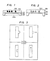
- Figs. 1 and 2 illustrate exemplary structures of such X-ray exposure mask (hereinafter referred to simply as X-ray mask).
- a thin film 202 of boron nitride BN is formed on a mask frame 201 composed of a silicon wafer with an X-ray pass window 201a and, after a plating electrode 101 permeable to X-rays is formed thereon, a heavy metal pattern 205 is formed by plating and then is coated with a protective film 204.
- a central portion of the mask frame 201 composed of a silicon wafer is removed by etching so that a window 201a is formed for achieving ready permeation of X-rays.
- a thin film 302 of silicon nitride or the like is formed on a mask frame 201 composed of a silicon substrate and, after a heavy metal 205 is deposited thereon, its pattern 303 is formed by dry etching and then is coated with a protective film 204.
- Fig. 3 illustrates examples of such defects, in which (a) represents a black spot defect where the pattern is deposited in excess, and (b) represents a white spot defect where the pattern is dropped out.
- the X-ray mask pattern is as fine as 0.5 ⁇ m or less and still has a height of 0.5 ⁇ m or more for absorbing X-rays.
- the present invention comprises the steps of initially forming a conductive film under a circuit pattern having a protective film like an X-ray absorbing metal (Au) pattern of an X-ray mask, subsequently boring the protective film in a dropout defective portion by the use of a high-intensity focused ion beam to expose the conductive film partially, and then plating the defective portion with a heavy metal while utilizing such exposed conductive film as a plating electrode, thereby correcting the dropout defect on the circuit pattern.
- a protective film like an X-ray absorbing metal (Au) pattern of an X-ray mask
- the feature of the present invention resides in that a dropout defective portion of a circuit pattern coated with a protective film is detected and then is irradiated with a high-intensity ion beam, so that a hole is bored accurately down to the vicinity of a conductive film formed under the circuit pattern, and the dropout defect on the circuit pattern is corrected by plating executed through such hole.
- any dropout defect where does not exist a circuit pattern in an X-ray mask or the like can be corrected within a short period of time to consequently render the X-ray mask satisfactory for practical use.
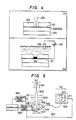
- Fig. 4 shows a means for correcting a white spot defect in an X-ray mask according to the present invention.
- a plating electrode 101 is formed immediately below a heavy metal circuit pattern 205 (303).
- a conductive material 101 is deposited correspondingly to the plating electrode.
- a protective film 204 is bored in its portion corresponding to the white spot defect by the use of a focused ion beam 502, whereby the conductive film 101 is partially exposed.
- the entire X-ray mask is immersed in a heavy metal plating solution (e.g. non-cyanic plating solution), and a voltage 107 is applied between the conductive film 101 and the heavy metal electrode 106 of the X-ray mask, so that a heavy metal film 108 is formed by the plating in the portion of the conductive film 101 exposed by previously boring the protective film 204 with an ion beam, thereby correcting the white spot defect.
- a heavy metal plating solution e.g. non-cyanic plating solution
- Fig. 5 shows a first embodiment designed to carry out the method of the present invention.
- An ion beam emitted from a fluid metal ion source 501 is converged by an electrostatic lens 503 and then is deflected by a combination of a blanking electrode 504 and a blanking apertur e 506, which are driven in response to a blanking signal 521 from a blanking power supply 520, and a deflection electrode 505 driven in response to a deflection signal 523 from a deflection power supply 522.
- the ion beam thus deflected is irradiated onto a workpiece 507.
- Denoted by 524 is a controller disposed for controlling the blanking power supply 520, the deflection power supply 522, the electrostatic lens 503 and so forth.
- secondary charged particles including secondary electrons and secondary ions
- a detector 508 a detector disposed for controlling the blanking power supply 520, the deflection power supply 522, the electrostatic lens 503 and so forth.
- secondary charged particles including secondary electrons and secondary ions
- a resultant scanned ion image is visually represented on a display 509 in accordance with the deflection signal 523, whereby the circuit pattern 510 and the defect 511 of the X-ray mask are detected.
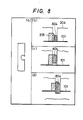
- the X-ray mask is generally so composed that the absorber (Au) circuit pattern 205 is coated with a protective film 204 of polyimide or the like.
- the protective film 204 is formed in a thickness of more than 1 ⁇ m on the upper portion of the absorber circuit pattern 205, but the surface unevenness of the protective film 204 is not conformable with that of the abosrber circuit pattern 205 therebelow.
- a wide area of the protective film 204 is scanned by an ion beam 701 and then the surface thereof is processed.
- the current flowing toward the detector 704 tends to overlap as denoted by reference numeral 706 in the case where the ion beam passes through the upper portion of the absorber circuit pattern 205 and in the place where the protective film 204 alone is existent without the absorber.
- Such tendency becomes more marked with reduction of the thickness t of the protective film 204 left on the absorber (Au) circuit pattern 205 posterior to the process.
- Fig. 8 (a) illustrates an exemplary defective circuit pattern with a white spot (dropout) defect.
- the protective film 204 is bored by a focused ion beam down to the conductive film 101 as illustrated in Fig. 8 (b), and in the next plating step, the lateral surface of the absorber metal pattern 205 also serves as a plating electrode in addition to the conductive film 101, so that a plating metal film grows therefrom as well.
- the conductive film needs to be thin for minimizing the amount of absorption of X-rays, and therefore it is difficult to interrupt the plating exactly in the region of the conductive film.
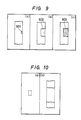
- Fig. 9 shows an example where a white spot defect is extremely small as 0.1 ⁇ m or so.
- a plating solution may fail to enter the hole formed in the protective film 204 of polyimide and consequently no plating film grows therein. Therefore, a wide area 902 surrounding the white spot defect is bored by a focused ion beam as illustrated in Fig. 9 (b), and subsequently a plating film 903 is formed as mentioned previously to perform rapid correction of the white spot defect.
- Fig. 11 illustrates how high-precision depth monitoring is executed for such purpose.
- the current indicates a small value (i) during the boring process of the protective film 204 as shown in Fig. 11 (b), but with gradual approach of the hole bottom to the conductive film, the current leaks through the remaining thin portion of the protective film and sharply increases in flowing into the conductive film 101 as represented by (ii).
- the boring can be terminated exactly upon arrival at the conductive film to eventually enable proper correction of the white spot defect with satisfactory plating.
- the monitoring is executed by detection of the current from the conductive film 101, it is also possible to achieve accurate monitoring by detection of the secondary electrons, secondary ions and fluorescent reflected electrons emitted from the workpiece (surface of X-ray mask) and the changes in the quantities thereof.
- Fig. 12 illustrates an embodiment for executing accurate depth monitoring as in the foregoing example.
- the protective film 204 is bored at a constant speed.
- the boring speed is high as represented by A ⁇ , and consequently the required time t2 - tl is short. Therefore it is difficult to attain high-precision depth monitoring on the basis of measuring such short boring time with the ion beam.
- the conductive-film boring speed is lowered to B ⁇ by replacing the ordinary material of the conductive film with another material such as nickel Ni of a lower sputtering rate, whereby the boring time is prolonged as t3 - tl.
- the monitoring can be executed with a high precision by controlling such boring time.
- the conductive film may be shaped into a multilayer structure which is composed of several kinds of metals.
- the same effect as mentioned can be attained by selectively employing a material of a lower sputtering rate to prolong the boring time.
- an additional step of forming another protective film of polyimide or the like may be carried out, if necessary, to protect the film in the portion corrected by the plating.
- the present invention can be applied also to a method which bores the protective film by a focused ion beam to make a hole or a slit therein and then forms a metal film in the bored portion by means of plating to correct the pattern.
- a dropout defect in a circuit pattern having a protective film such as an X-ray mask or the like can be corrected with safety and at low cost practically without causing contamination of a vacuum receptacle, an ion source or an ion-beam optical system.
- the required correction time can be shortened since a great quantity of X-ray masks can be plated and corrected at a time.
Landscapes
- Physics & Mathematics (AREA)
- General Physics & Mathematics (AREA)
- Preparing Plates And Mask In Photomechanical Process (AREA)
- Exposure Of Semiconductors, Excluding Electron Or Ion Beam Exposure (AREA)
Applications Claiming Priority (2)
| Application Number | Priority Date | Filing Date | Title |
|---|---|---|---|
| JP42542/87 | 1987-02-27 | ||
| JP62042542A JPS63210845A (ja) | 1987-02-27 | 1987-02-27 | 欠陥修正方法 |
Publications (3)
| Publication Number | Publication Date |
|---|---|
| EP0280131A2 true EP0280131A2 (de) | 1988-08-31 |
| EP0280131A3 EP0280131A3 (en) | 1989-10-11 |
| EP0280131B1 EP0280131B1 (de) | 1992-01-15 |
Family
ID=12638951
Family Applications (1)
| Application Number | Title | Priority Date | Filing Date |
|---|---|---|---|
| EP88102080A Expired - Lifetime EP0280131B1 (de) | 1987-02-27 | 1988-02-12 | Korrektionsverfahren für Schaltungspatrone |
Country Status (4)
| Country | Link |
|---|---|
| US (1) | US4925755A (de) |
| EP (1) | EP0280131B1 (de) |
| JP (1) | JPS63210845A (de) |
| DE (1) | DE3867651D1 (de) |
Families Citing this family (16)
| Publication number | Priority date | Publication date | Assignee | Title |
|---|---|---|---|---|
| JPH0262039A (ja) * | 1988-08-29 | 1990-03-01 | Hitachi Ltd | 多層素子の微細加工方法およびその装置 |
| EP0361516B1 (de) * | 1988-09-30 | 1996-05-01 | Canon Kabushiki Kaisha | Verfahren zur Herstellung einer Röntgenstrahlmasken-Struktur |
| US5246804A (en) * | 1988-11-08 | 1993-09-21 | Kyodo Printing Co., Ltd. | Method of retouching pattern |
| JP2710967B2 (ja) | 1988-11-22 | 1998-02-10 | 株式会社日立製作所 | 集積回路装置の製造方法 |
| JPH03102352A (ja) * | 1989-09-18 | 1991-04-26 | Hitachi Ltd | パターン形成方法 |
| JP2655215B2 (ja) * | 1991-11-18 | 1997-09-17 | 三菱電機株式会社 | フォトマスクのパターン欠陥修正方法 |
| US5235154A (en) * | 1992-04-28 | 1993-08-10 | International Business Machines Corporation | Laser removal of metal interconnects |
| US6897440B1 (en) * | 1998-11-30 | 2005-05-24 | Fab Solutions, Inc. | Contact hole standard test device |
| US6670717B2 (en) * | 2001-10-15 | 2003-12-30 | International Business Machines Corporation | Structure and method for charge sensitive electrical devices |
| US7674706B2 (en) * | 2004-04-13 | 2010-03-09 | Fei Company | System for modifying small structures using localized charge transfer mechanism to remove or deposit material |
| US8278220B2 (en) * | 2008-08-08 | 2012-10-02 | Fei Company | Method to direct pattern metals on a substrate |
| JP2011146690A (ja) * | 2009-12-18 | 2011-07-28 | Canon Anelva Corp | イオンビーム発生装置及びこれを用いた基板処理装置と電子デバイス製造方法 |
| US9255339B2 (en) | 2011-09-19 | 2016-02-09 | Fei Company | Localized, in-vacuum modification of small structures |
| CN104345548B (zh) * | 2013-07-31 | 2018-07-20 | 中芯国际集成电路制造(上海)有限公司 | 亚微米级掩模版的制造方法 |
| US11448467B1 (en) | 2018-09-28 | 2022-09-20 | Clean Energy Systems, Inc. | Micro-tube metal matrix heat exchanger and method of manufacture |
| US11503224B1 (en) * | 2021-11-29 | 2022-11-15 | Unity Technologies Sf | Increasing dynamic range of a virtual production display |
Family Cites Families (12)
| Publication number | Priority date | Publication date | Assignee | Title |
|---|---|---|---|---|
| JPS5423473A (en) * | 1977-07-25 | 1979-02-22 | Cho Lsi Gijutsu Kenkyu Kumiai | Photomask and method of inspecting mask pattern using same |
| US4328298A (en) * | 1979-06-27 | 1982-05-04 | The Perkin-Elmer Corporation | Process for manufacturing lithography masks |
| JPS5693323A (en) * | 1979-12-26 | 1981-07-28 | Nec Corp | Correcting method for photomask using laser beam and device thereof |
| JPS57210629A (en) * | 1981-06-19 | 1982-12-24 | Fujitsu Ltd | Correcting method for photo-mask pattern |
| JPS5852821A (ja) * | 1981-09-24 | 1983-03-29 | Fujitsu Ltd | ハ−ドマスクの修正法 |
| JPS5856332A (ja) * | 1981-09-30 | 1983-04-04 | Hitachi Ltd | マスクの欠陥修正方法 |
| JPS58111317A (ja) * | 1981-12-25 | 1983-07-02 | Oki Electric Ind Co Ltd | フオトマスクの修正方法 |
| JPS59169133A (ja) * | 1983-03-16 | 1984-09-25 | Hitachi Ltd | パタ−ン修正装置 |
| JPS60234320A (ja) * | 1984-05-08 | 1985-11-21 | Hitachi Ltd | フオトマスクの欠陥修正方法及び装置 |
| JPS6158233A (ja) * | 1984-08-29 | 1986-03-25 | Fujitsu Ltd | X線リソグラフイ−用マスク |
| JPS61111526A (ja) * | 1984-10-11 | 1986-05-29 | Sharp Corp | マスクパタ−ンの欠陥修正方法 |
| DE3576088D1 (de) * | 1985-05-29 | 1990-03-29 | Ibm Deutschland | Verfahren zur reparatur von transmissionsmasken. |
-
1987
- 1987-02-27 JP JP62042542A patent/JPS63210845A/ja active Pending
-
1988
- 1988-02-04 US US07/152,159 patent/US4925755A/en not_active Expired - Lifetime
- 1988-02-12 DE DE8888102080T patent/DE3867651D1/de not_active Expired - Lifetime
- 1988-02-12 EP EP88102080A patent/EP0280131B1/de not_active Expired - Lifetime
Also Published As
| Publication number | Publication date |
|---|---|
| DE3867651D1 (de) | 1992-02-27 |
| EP0280131B1 (de) | 1992-01-15 |
| US4925755A (en) | 1990-05-15 |
| JPS63210845A (ja) | 1988-09-01 |
| EP0280131A3 (en) | 1989-10-11 |
Similar Documents
| Publication | Publication Date | Title |
|---|---|---|
| EP0280131B1 (de) | Korrektionsverfahren für Schaltungspatrone | |
| US4683378A (en) | Apparatus for ion beam work | |
| US6583634B1 (en) | Method of inspecting circuit pattern and inspecting instrument | |
| US4609809A (en) | Method and apparatus for correcting delicate wiring of IC device | |
| EP0334680B1 (de) | Korrekturverfahren für Maske | |
| US4933565A (en) | Method and apparatus for correcting defects of X-ray mask | |
| US7521679B2 (en) | Inspection method and inspection system using charged particle beam | |
| JPH09283496A (ja) | 荷電粒子ビーム照射によるパターン形成方法及びその装置 | |
| US6642528B2 (en) | Alignment mark detection method, and alignment method, exposure method and device, and device production method, making use of the alignment mark detection method | |
| EP0104763B1 (de) | Mit einem Autofokussierungsmechanismus ausgestattetes Musterübertragungssystem | |
| US4316093A (en) | Sub-100A range line width pattern fabrication | |
| US5004927A (en) | Process for forming a fine pattern having a high aspect ratio | |
| JP2565121B2 (ja) | 電子線直接描画方法 | |
| JPH05215696A (ja) | 欠陥検査方法および装置 | |
| JP2519512B2 (ja) | 集束イオンビ―ム装置 | |
| JP2619435B2 (ja) | イオンビーム加工方法 | |
| KR100511816B1 (ko) | 반도체 제조 방법 및 플라즈마 처리 방법 및 그 장치 | |
| JPS6269527A (ja) | 検査装置 | |
| US7060397B2 (en) | EPL mask processing method and device thereof | |
| JPS6146965B2 (de) | ||
| JP2746554B2 (ja) | イオンビーム除去加工方法及びその装置並びにイオンビーム局所成膜方法及びその装置 | |
| JP2525221B2 (ja) | マスク修正装置 | |
| JP2000058473A (ja) | 半導体製造装置 | |
| JP2000036278A (ja) | Fib操作の自動シ―ケンス動作 | |
| JPH04257216A (ja) | X線マスク |
Legal Events
| Date | Code | Title | Description |
|---|---|---|---|
| PUAI | Public reference made under article 153(3) epc to a published international application that has entered the european phase |
Free format text: ORIGINAL CODE: 0009012 |
|
| AK | Designated contracting states |
Kind code of ref document: A2 Designated state(s): DE FR GB |
|
| PUAL | Search report despatched |
Free format text: ORIGINAL CODE: 0009013 |
|
| AK | Designated contracting states |
Kind code of ref document: A3 Designated state(s): DE FR GB |
|
| 17P | Request for examination filed |
Effective date: 19890829 |
|
| 17Q | First examination report despatched |
Effective date: 19910507 |
|
| GRAA | (expected) grant |
Free format text: ORIGINAL CODE: 0009210 |
|
| AK | Designated contracting states |
Kind code of ref document: B1 Designated state(s): DE FR GB |
|
| REF | Corresponds to: |
Ref document number: 3867651 Country of ref document: DE Date of ref document: 19920227 |
|
| ET | Fr: translation filed | ||
| PLBE | No opposition filed within time limit |
Free format text: ORIGINAL CODE: 0009261 |
|
| 26N | No opposition filed | ||
| PGFP | Annual fee paid to national office [announced via postgrant information from national office to epo] |
Ref country code: GB Payment date: 19940202 Year of fee payment: 7 |
|
| PGFP | Annual fee paid to national office [announced via postgrant information from national office to epo] |
Ref country code: FR Payment date: 19940217 Year of fee payment: 7 |
|
| PGFP | Annual fee paid to national office [announced via postgrant information from national office to epo] |
Ref country code: DE Payment date: 19940428 Year of fee payment: 7 |
|
| PG25 | Lapsed in a contracting state [announced via postgrant information from national office to epo] |
Ref country code: GB Effective date: 19950212 |
|
| GBPC | Gb: european patent ceased through non-payment of renewal fee |
Effective date: 19950212 |
|
| PG25 | Lapsed in a contracting state [announced via postgrant information from national office to epo] |
Ref country code: FR Effective date: 19951031 |
|
| PG25 | Lapsed in a contracting state [announced via postgrant information from national office to epo] |
Ref country code: DE Effective date: 19951101 |
|
| REG | Reference to a national code |
Ref country code: FR Ref legal event code: ST |