EP0277657A2 - Appareil d'affichage d'images - Google Patents
Appareil d'affichage d'images Download PDFInfo
- Publication number
- EP0277657A2 EP0277657A2 EP88101621A EP88101621A EP0277657A2 EP 0277657 A2 EP0277657 A2 EP 0277657A2 EP 88101621 A EP88101621 A EP 88101621A EP 88101621 A EP88101621 A EP 88101621A EP 0277657 A2 EP0277657 A2 EP 0277657A2
- Authority
- EP
- European Patent Office
- Prior art keywords
- picture
- character
- pictures
- output
- block
- Prior art date
- Legal status (The legal status is an assumption and is not a legal conclusion. Google has not performed a legal analysis and makes no representation as to the accuracy of the status listed.)
- Granted
Links
Images


Classifications
-
- H—ELECTRICITY
- H04—ELECTRIC COMMUNICATION TECHNIQUE
- H04N—PICTORIAL COMMUNICATION, e.g. TELEVISION
- H04N5/00—Details of television systems
- H04N5/66—Transforming electric information into light information
- H04N5/68—Circuit details for cathode-ray display tubes
-
- G—PHYSICS
- G09—EDUCATION; CRYPTOGRAPHY; DISPLAY; ADVERTISING; SEALS
- G09G—ARRANGEMENTS OR CIRCUITS FOR CONTROL OF INDICATING DEVICES USING STATIC MEANS TO PRESENT VARIABLE INFORMATION
- G09G5/00—Control arrangements or circuits for visual indicators common to cathode-ray tube indicators and other visual indicators
- G09G5/02—Control arrangements or circuits for visual indicators common to cathode-ray tube indicators and other visual indicators characterised by the way in which colour is displayed
- G09G5/026—Control of mixing and/or overlay of colours in general
-
- G—PHYSICS
- G09—EDUCATION; CRYPTOGRAPHY; DISPLAY; ADVERTISING; SEALS
- G09G—ARRANGEMENTS OR CIRCUITS FOR CONTROL OF INDICATING DEVICES USING STATIC MEANS TO PRESENT VARIABLE INFORMATION
- G09G5/00—Control arrangements or circuits for visual indicators common to cathode-ray tube indicators and other visual indicators
- G09G5/22—Control arrangements or circuits for visual indicators common to cathode-ray tube indicators and other visual indicators characterised by the display of characters or indicia using display control signals derived from coded signals representing the characters or indicia, e.g. with a character-code memory
- G09G5/222—Control of the character-code memory
Definitions
- the present invention relates to an image display apparatus and, more particularly, to an image display apparatus for synthesizing one color picture from a plurality of overlapping pictures and outputting the synthesized picture.
- Image display apparatus which adopt a dot-map-display system or a character block system have convectionally been known and widely used for synthesizing and outputting various pictures to be displayed on a CRT.
- a picture displayed on a CRT for games is generally composed of 224 horizontal scanning lines, and each line is composed of picture elements of 288 dots.
- One picture of such a picture to be displayed on a CRT is therefore composed of picture elements of 288 ⁇ 224 dots, and in order to display 256 colors on the CRT, it is necessary that a color corresponds to color data of 8 bits which designate the color for each dot.
- a dot-map-memory of as large a capacity as 288 (the number of dots per line) ⁇ 224 (the number of horizontal scanning lines) ⁇ 8 (color code) is inconveniently necessary in order to display one picture.
- the picture to be displayed on the CRT is often selected by scrolling vertically and horizontally in the scroll reference picture which displays the object of display.
- CRT display picture In the case where the picture to be displayed on the CRT (hereinunder referred to as "CRT display picture") is determined while scrolling in this way, it is often the case that the scroll reference picture has such a large square configuration as 512 ⁇ 512 dots. If a color code of 8 bits is set for each dot of such a large scroll reference picture, the capacity of the dot-map-memory becomes disadvantageously large.
- an image display apparatus of a character block system a picture to be displayed on a CRT is divided into a plurality of character blocks, so that the CRT display picture is efficiently synthesized and output with a memory of a small capacity.
- the present invention relates to an image display apparatus of this system.
- a CRT display picture is divided by a unit of a character block 100 of an 8 dot ⁇ 8 dot square, as shown in Fig. 7(B)
- the CRT display picture is divided vertically into 36 blocks and horizontally 28 blocks, namely, into 36 ⁇ 28 character blocks in total, as shown in Fig. 7(A).
- Fig. 8 shows the principle of an image display apparatus of a character block system in the prior art which has been widely used.
- the image display apparatus is provided with a character generator 10 in which a plural items of character data are registered in advance which are to be displayed in the corresponding character block 100.
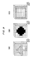
- Figs. 9(A) to 9(C) respectively show examples of color data registered in advance in the character generator 10.
- Each item of character data is composed as an item of color data which fills in the character block 100 of 8 dots ⁇ 8 dots.
- the above-described conventional apparatus includes a video RAM 12 serving as a picture display memory, a CRT controller 14 and a latch circuit 16.
- a video RAM 12 serving as a picture display memory
- a CRT controller 14 controls the video RAM 12
- a latch circuit 16 controls the video RAM 12
- an address for reading a color character which is to be displayed in the corresponding character block is registered in each character block address.
- the CRT controller 14 outputs a character block address signal 200 in synchronization with horizontal and vertical scans of the CRT.
- the video RAM 12 then reads a color character read address signal 210 which has been registered in advance and outputs it to the character generator 10 through the latch circuit 16.
- the character generator 10 outputs the color character data designated by the read address signal 210 to a parallel-serial conversion circuit 18.
- Each item of character color data registered in the character generator 10 is composed of a combination of 8 lines of horizontal scanning information, each line consisting of 8 dots, as shown in Figs. 9(A) to 9(C).
- the CRT controller 12 therefore outputs a vertical scanning position address signal 220 in each character block 100 to the character generator 10 in synchronization with the horizontal and vertical scans.
- the character read address 210 when an item of character color data such as that shown in Fig. 9 is designated by the character read address 210, the color character data for one line which is designated by the vertical scanning position address signal 220 is read from the character generator 10 to the parallel-serial conversion circuit 18. The thus-read out color character data for one line (A) is output as a video signal 230 in synchronization with the horizontal scan of the CRT.
- the CRT controller 14 outputs the character block address signal 200 which designates the character block 100-1 to the video RAM 12.
- the video RAM 12 outputs the color character read address signal 210 for reading the color character data shown in Fig. 9(A) to the character generator 10 through the latch circuit 16.
- the CRT controller 14 outputs the vertical scanning position address signal 220 which indicates the third line scan to the character generator 10.
- the character generator 10 outputs the data at the third line of the color character data shown in Fig. 9(A) to the parallel-serial conversion circuit 18 as a parallel signal.
- the parallel-serial conversion circuit 18 consecutively outputs an item of character color data for one line as a video signal 230 for each dot in synchronization with the horizontal scan of the CRT.
- the CRT controller 14 When the horizontal scan of the eighth dot of the CRT is finished in this way, the CRT controller 14 outputs the address signal 200 which designates the next character block 100-2 to the video RAM 12 in the same way, and the vertical scanning position address 220 which indicates the horizontal scan of the third line to the character generator 10 in the same way.
- the character generator 10 therefore outputs the character color data at the third line of the character block 100-2 as the video signal 230 through the parallel-serial conversion circuit 18.
- this image display apparatus has a structure in which color character data to be used are registered in the character generator 10 in advance and only the color character read addresses 210 for the color characters to be displayed in the corresponding character blocks are registered in the video RAM 12, the memory capacity of the video RAM 12 is much smaller than that of the image display apparatus of the dot-map-display system, and the structure of the image display apparatus is simplified in comparison with that of the image picture display apparatus of the dot-map-display system.
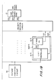
- Such an image display apparatus of a character block system is often used for synthesizing one color picture by placing a plurality of pictures with one on top of another.
- the image display apparatus is used for laying a top picture 300-1 on a bottom picture 300-2 for displaying a synthesized picture 400.
- Fig. 11 shows an example of such an image display apparatus for synthesizing a picture by placing a plurality of pictures with one on top of another.
- the same numerals are provided for the elements which correspond to those shown in Fig. 8, and explanation thereof will be omitted.
- the three pictures are generally formed by using three picture formation circuits 500-1, 500-2 and 500-3.
- the video signals 230-0, 230-1 and 230-2 which are output from the respective picture formation circuits 500-0, 500-1 and 500-2 are output to a priority decision circuit 20.
- the priority decision circuit 20 compares the video signals 230-0, 230-1 and 230-2 in each dot which are output from the respective picture formation circuits 500-0, 500-1 and 500-2 in accordance with predetermined priorities, and the signal which is judged to have the highest priority is output as a video signal 240 for picture synthesis.
- the pictures are determined to have a priority in the order of 300-0, 300-1, and 300-2, and character codes "0008H", "0009H” and "000AH" which correspond to the character data shown in Figs. 9(A), 9(B) and 9(C), respectively, are respectively registered in the first character blocks of the respective pictures, the color characters are displayed in the first character block 100-1 of the CRT display picture which is indicated by the video signal 240 with the color characters placed with one on top of another in the order of priority, as shown in Fig. 13.
- the conventional image display apparatus of a character block system is very suitable for synthesizing one picture from a plurality of overlapping pictures, because the memory capacity (capacity of the video RAM) required for synthesizing one picture is very small.
- the priority decision circuit 20 compares 8-bit color data in each dot in order to determine the priorities of the video signals 230 output from the respective picture formation circuits 500-0, 500-1, 500-2, ..., and the circuitry structure of the priority decision circuit 20 becomes complicated and, in addition, processing of determining the priority takes a long time.
- the present invention provides a picture display apparatus for synthesizing one color picture by placing a plurality of pictures with one on top of another, comprising: a picture display memory for dividing each of the pictures before synthesis into a plurality of character blocks, and registering addresses for reading the color characters to be displayed in the respective character blocks at the respective character block addresses; a raster display controller for successively outputting the character block address signals of the respective pictures before synthesis to said picture display memory in synchronization with horizontal and vertical scans of a raster display so that said picture display memory successively outputs the corresponding character read address signals in the numerical order of said pictures, and for successively outputting vertical scanning position address signals for the corresponding character blocks of the respective pictures; a shape generator in which a plurality of character shapes to be displayed in the respective character blocks are registered in advance, and which outputs, in the numerical order of said pictures, character shape data for one horizontal scan of the character blocks which are designated by the corresponding vertical scanning position address signals in
- the image display apparatus according to the present invention is sufficed with only one character generator, the space in the apparatus occupied by the character generator is small.
- the space occupied by the character generator is much smaller than that in the conventional apparatus, thereby enabling efficient arrangement of circuitry.
- the shape data (data including no color information) output from a shape generator are compared with each other in accordance with predetermined priorities in order to determine the priorities of the plurality of pictures which are displayed in an overlapping state in each dot.
- the priority is therefore determined in each dot only by the processing of an item of shape data (information as to whether or not the dot is transparent) of 1 bit.
- the image display apparatus is capable of executing the arithmetic processing for synthesizing and outputting one color picture with a much simpler structure and a higher speed than the conventional apparatus and, in addition, it is possible to manufacture the apparatus itself at a lower cost.
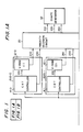
- Fig. 1 shows a preferred embodiment of an image display apparatus according to the present invention.
- the apparatus of this embodiment includes six picture formation circuits 500-0, 500-1, ... 500-5.
- Each picture formation circuit 500 is composed of a CRT controller 14 and a video RAM 12 serving as a picture display memory.
- Fig. 2 shows the relationship between the image in each picture formed by using each of the picture formation circuits 500-0, 500-1, .... 500-5 and the video RAM 12.
- the video RAMs 12-0, 12-1, ... 12-5 provided in the picture formation circuits 500-0, 500-1, ... 500-5, respectively, are composed of six divisions of the storage region of the video RAM 12 which is divided by predetermined addresses, as shown in Fig. 2.
- the video RAMs 12-0, 12-1 and 12-2 are used for forming scroll reference pictures 600-0, 600-1 and 600-2, respectively, each having 64 character blocks in the vertical direction and 64 character blocks in the horizontal direction.
- a character read address 210 necessary for reading color character data which are to be displayed in the respective scroll reference pictures from a character generator 10 is registered in each of the video RAMs 12-0, 12-1 and 12-2.
- the data on a scroll reference picture 600-3 having a rectangular configuration of 32 character blocks in the vertical direction and 64 character blocks in the horizontal direction are registered in the same way.
- the data on the scroll reference pictures 600-0, 600-1, ... 600-3 are registered in the respective video RAMs 12-0, ... 12-3 of the respective picture formation circuits 500-0 to 500-3. It is therefore necessary to designate the pictures 300-0, 300-1, ... 300-3 to be displayed on the CRT from the respective scroll reference pictures.
- the fixed pictures 600-4 and 600-5 are registered, as described above, which are displayed as they are on the CRT as the CRT display pictures 300-4 and 300-5.
- the apparatus of this embodiment is therefore provided with a picture computing circuit 30 for designating the CRT display pictures 300-0, 300-1, ... 300-3 from the scroll reference pictures 600-0, 600-1, ... 600-3, respectively, and the designation signals are output from the picture computing circuit 30 to the CRT controllers 14 of the respective picture formation circuits.
- the character read address signal 210 and a vertical scanning position address signals 220 of the corresponding character block which are necessary for forming the CRT display pictures 300-0, 300-1, ... 300-3 are output from each of the picture formation circuits 500-0, 500-1, ... 500-3, respectively, to a priority decision circuit 20.
- the first characteristic feature of the present invention is that the image display apparatus is provided with a shape generator 32 in which plural items of character shape data which are displayed in the corresponding character blocks are registered in advance.
- the shape generator 32 outputs character shape data 250 for one horizontal scan of the character block which is designated by the vertical scanning position address signal 220 (shape data for a horizontal scan of 8 dots) in accordance with the character shape data which are designated by the character read address signal 210 every time the address signal 210 and the vertical scanning position address signal 220 are output from each of the picture formation circuits 500-0, 500-1, ... 500-5.
- the priority decision circuit 20 compares the character shape data 250 of the respective pictures which are output from the shape generator 32 in this way with each other in each dot in accordance with predetermined priorities. During the horizontal scan of each character block of the CRT, the priority picture to be displayed on the CRT is determined in each dot.
- the character shape data 250 for one horizontal scan which is compared with another character shape data 250 is information as to whether or not the corresponding dot is transparent, so that data of 1 bit is sufficient for one dot.
- the necessary amount of character shape data 250 for one horizontal scan which is output from the shape generator 32 is 1/8 the amount of color character data for one horizontal scan which is output from the character generator 10 in the same way. It is therefore possible to greatly shorten the arithmetic processing time required for determining the priority picture by comparing plural items of character shape data output from the shape generator 32, as described above. In addition, since the amount of data to be processed is small, it is possible to simplify the structure of the priority decision circuit to a large extent.
- the second characteristic feature of the present invention is that the utilization of the results of the priority decision circuit enables the one character generator 10 to synthesize one color picture by placing a plurality of pictures with one on top of another.
- the priority decision circuit 20 determines the priority picture which is to be displayed on the CRT for each dot, the priority decision circuit 20 inputs the character read address signal 210, the vertical scanning position address signal 220 and the horizontal scanning position address signal 260 for the character generator block which are output from the picture formation circuit 500 in the character generator 10 in correspondence with the priority picture.
- the character generator read address signal 210 informs the character generator 10 of the designated color character data.
- the character generator 10 then outputs color data for one dot which are specified by the vertical scanning position (vertical scanning position address signal 220) and the horizontal scanning position (horizontal scanning position address signal 260) as the video signal 240 for picture synthesis.
- the one character generator 10 successively outputs the color data for the dot which indicates the scanning position as the video signal 240 in synchronization with the horizontal scanning and the vertical scanning of the CRT, thereby synthesizing one color picture.
- the one character generator 10 is sufficient even if the number of the overlapping pictures is increased, so that the effect of reducing the cost in comparison with a conventional apparatus is heightened as the number of the overlapping pictures is increased.
- the only one character generator 10 is used according to the present invention, it is possible to register the color character data which are to be displayed in the corresponding character blocks of the pictures 600-0, 600-1, ... 600-5 without overlapping as in a conventional apparatus and, hence, to utilize the memory space in the character generator with efficiency.
- the space in the interior of the apparatus which is occupied by the character generator 10 is small, thereby enabling comparatively free and efficient arrangement of circuitry in the limited space.
- Figs. 3 and 4 show the structure of the circuitry of another embodiment of an image display apparatus according to the present invention.
- Fig. 3 shows the structure of the picture formation circuit. 500 used in this embodiment.
- This embodiment is characterized in that the plurality of picture formation circuits 500-0, 500-1, ... 500-5 shown in Fig. 1 are formed as one picture formation circuit 500 by using the technique of time sharing.
- the picture formation circuit 500 is so composed as to output the character read address signals 210 and the vertical scanning position address signals 220 of the respective pictures 600-0, 600-1, ... 600-5 in that order in synchronization with the horizontal and vertical scans of the CRT.
- the picture formation circuit 500 in this embodiment is composed of the one CRT controller 14 and the video RAM 12 serving as the picture display memory.
- the memory region of the video RAM 12 is divided into six regions by predetermined addresses, as shown in Fig. 2.
- the character read address of the corresponding scroll reference picture 600-0, 600-1, ... or 600-3 or the corresponding fixed picture 600-4 or 600-5 is registered in the same way as in the video RAMs 12-0, 12-1, ... 12-5 shown in Fig. 1.
- the character read address 210 is composed of data of 2 bytes, and each byte of data is registered in the two consecutive character block addresses in the video RAM 12.
- the CRT controller 14 includes a first block address generation circuit 34 and a second block address generation circuit 36 and selectively outputs the signals output from these block address generation circuits 34 and 36 to an address computing circuit 40 through a multiplexer 38.
- the first block address generation circuit 34 generates block addresses for the scroll reference pictures 600-0, 600-1, ... 600-3 shown in Fig. 2.
- the second block address generation circuit 36 generates block addresses for the fixed pictures 600-4 and 600-5.
- the first block address generation circuit 34 in this embodiment is composed of a horizontal block computing circuit 42 for outputting a signal 700a which indicates the block position in the horizontal direction of the corresponding scroll reference picture 600-0, 600-1, ... or 600-3, and a vertical position computing circuit 44 for outputting a signal 700b which indicates the vertical position of the scanning line in the corresponding scroll reference picture 600-0, 600-1, ... or 600-3.
- the horizontal block computing circuit 42 is composed of four block displacement latch circuits 46-0, 46-1, 46-2 and 46-3 which correspond to the respective scroll reference pictures, a multiplexer 48 for selectively switching and outputting the output of each latch circuit 46 at a predetermined timing, an H counter 50 for increasing the count value by one at the end of every horizontal scan of one block of the CRT and an adder 52 for adding the output of the H counter 50 and the output of the multiplexer 48 and outputting the signal 700a which indicates the block position in the horizontal direction of the corresponding scroll reference picture.
- the vertical position computing circuit 44 is composed of four latch circuits 54-0, 54-1, 54-2 and 54-3 for setting the dot displacements relative to the vertical direction of the scroll reference pictures 600-0, 600-1, ... 600-3, respectively, a multiplexer 56 for selectively outputting the output of each latch circuit 54 at a predetermined timing, a V counter for increasing the count value by one at the end of every horizontal scan of the picture to be displayed in the CRT and an adder 60 for adding the output of the V counter 58 and the output of the multiplexer 56 and outputting the signal 700b which indicates the vertical position of the scanning line in the scroll reference picture 600.
- the displacements relative to the horizontal direction of the CRT display pictures 300-0, 300-1, ... 300-3, respectively, are set in blocks, and the displacements in blocks in this way are set in the displacement latch circuits 46-0, 46-1, ... 46-3, respectively, which correspond to the respective pictures.
- the displacements relative to the vertical direction of the CRT display pictures 300-0, 300-1, ... 300-3, respectively, are set in dots, and the displacements set in dots in this way are set in the displacement latch circuits 54-0, 54-1, ... 54-3, respectively, which correspond to the respective pictures.
- the adders 52 and 60 successively output the signals 700a which indicate the block positions in the horizontal direction of the scroll reference pictures 600-0, 600-1, ... 600-3 and the signals 700b which indicate the vertical positions of the scanning lines in correspondence with the scroll reference pictures 600-0, 600-1, ... 600-3 in that order.
- the second block generation circuit 36 outputs a signal 700c which indicates the position of the character block itself of the corresponding fixed picture 600-4 or 600-5 shown in Fig. 2.
- the multiplexer 38 outputs the pairs of signals 700a and 700b to the address computing circuit 40 which are successively output from the first block address generation circuit 34 in correspondence with the scroll reference pictures 600-0, 600-1, 600-2 and 600-3 in that order.
- the multiplexer 38 thereafter outputs the signals 700c to the address computing circuit 40 which are output from the second block address generation circuit 36 in correspondence with the fixed pictures 600-4 and 600-5 in that order.
- the signals 700 are successively input in the address computing circuit 40 in correspondence with the pictures 600-0, 600-1, ... 600-5 in that order.
- the CRT controller 14 in this embodiment is provided with a picture number generation circuit 62 for outputting the identification number 900 (identification number of the memory space in the video RAM 12) of the picture which corresponds to the signal 700 which is selectively output from the multiplexer 38.
- the picture number generation circuit 62 also outputs a signal 950 which designates the upper 1 byte and the lower 1 byte of the character read address signal 210 for the character to be displayed in the picture identified by the picture number generation circuit 62.
- the address computing circuit 40 are input the picture identification numbers 900 which are successively output from the picture number generation circuit 62 in correspondence with the pictures 600-0, 600-1, ... 600-5 in that order, the signal 950 for designating the upper 1 byte and the lower 1 byte of each character read address signal 210, and the signal 700 which is output through the multiplexer 38 in correspondence with the signal 950.
- the address computing circuit 40 On the basis of the signals input in this way and in synchronization with the horizontal and vertical scans of the CRT, the address computing circuit 40 successively computes the character block address signals 200 for designating the respective character blocks 100, the signals 950 for designating the upper 1 byte and the lower 1 byte of the character read addresses which are registered in the corresponding character blocks and outputs these signals (the signal obtained by combining the signals 200 and 950 constitutes the read address of the video RAM 12) to the video RAM 12 in correspondence with the CRT display pictures 300-0, 300-1, ... 300-5 in that order.
- the address computing circuit 40 also computes the vertical scanning position address signal 220 in each character block 100, and outputs the result as information of 3 bits through a line flip flop 64.
- the video RAM 12 outputs the read address signals 210 for the characters which are to be displayed in the corresponding character blocks on the basis of the input character block address signals 200 in correspondence with the CRT display pictures 300-0, 300-1, ... 300-5 in that order.
- the line flip flop 64 outputs the vertical scanning position address signal 220 corresponding to the read address signal 210 which is being output.
- the CRT controller 14 in this embodiment is also provided with a CPU address mixing circuit 66, which sets and registers a new character read address signal 210, if necessary, in a predetermined address under the instruction of the CPU by utilizing the spare time of the multiplexer 38 and the address computing circuit 40.
- the character read address signal 210 registered in the video RAM 12 is composed of data of 2 bytes, as described above. Accordingly, when the character block address signal 200 is output from the address computing circuit 40 together with the signal 950 from the picture number generation circuit 62, the video RAM 12 outputs the corresponding read address signal 210 twice, 1 byte at each time.
- the read address signal 210 of 1 byte output first from the video RAM 12 is therefore temporarily latched in a latch circuit 70, as shown in Fig. 4.
- the first read address signal 210 latched in the latch circuit 70 is output to a flip flop 72, while the second read address signal 210 is output to a flip flop 74.
- the read address signal 210 of 2 bytes which are respectively set in the flip flops 72 and 74 in this way is output to a 19-bit flip flop 76 which constitutes a part of the shape generator 32 and the priority decision circuit 20.
- the flip flop 64 outputs the vertical scanning position address signal 220 of 3 bits which correspond to the read address signal 210 to the shape generator 32 and the 19-bit flip flop 76.
- the read address signal 220 and the corresponding vertical scanning position address signal 210 are input.
- the character shape data 250 for one horizontal scan of the character block which is designated by the vertical scanning position address signal 220 from among the character shape data which are designated by the character read address signal 210 are output from the shape generator 32 to an 8-bit flip flop 78 in the priority decision circuit 20.
- the priority decision circuit 20 is provided with six picture data storage circuits 80-0, 80-1, ... 80-5 which correspond to the six CRT display pictures 300-0, 300-1, ... 300-5, respectively, which are shown in Fig. 2.
- the picture data storage circuit 80 is selected in correspondence with picture 300 containing the character read address signal 210 which is being output from the flip flops 72 and 74.
- the character read address signals 210 output from the flip flops 72 and 74 are input the character read address signals 210 output from the flip flops 72 and 74, the vertical scanning position address signal 220 output from the line flip flop 64 and the character shape data 250 for one horizontal scan output from the shape generator 32.
- each picture data storage circuit 80 is composed of the 19-bit flip flop 76, the 8-bit flip flop 78, a 16-bit flip flop 82, an 8-bit shift register 84, a 3-bit cyclic counter 86 and a latch circuit 88 for setting the displacement in the horizontal direction.
- the read address signal 210 for the corresponding picture is output from the pair of flip flops 72 and 74, the read address signal 210 and the vertical scanning position address signal 220 are input in the 19-bit flip flop 76, as described above. In the 16-bit flip flop 82, only the character read address signal 210 is input from the 19-bit flip flop 76.
- the character shape data 250 for one horizontal scan of the character block of the corresponding picture is input, as described above.
- the 3-bit cyclic counter 86 outputs the command of writing the data 250 in the 8-bit flip flop 78 to the 8-bit shift register 84 every time the count value becomes 0.
- the displacement in the horizontal direction is written into the latch circuit 88 from the outside through a data bus, and the 3-bit cyclic counter 86 cyclically counts the horizontal scanning synchronized signals by adding one with the displacement written in the latch circuit as the initial value every time the horizontal scanning synchronized signal for one dot is output.
- the initial values of the respective counters 86 are set at the timings of TM1 to TM0 corresponding to the respective pictures, which are shown in Fig. 6 and will be described later.
- the 3-bit cyclic counter 86 counts cyclically in the order of 2 ⁇ 3 ⁇ 4 ⁇ 5 ⁇ 6 ⁇ 7 ⁇ 8 ⁇ 0 ⁇ 1 in synchronization with a horizontal scan of the CRT, and every time the count value becomes 0, the above-described write command is output to the shift register 84.
- Fig. 6 shows the timing chart of this embodiment.
- a clock pulse of 6 MHz is used as the horizontal scanning synchronized signal for executing a horizontal scan of the CRT.
- one dot of the CRT is scanned for the time T which corresponds to one period of the synchronized signal.
- the timing chart shown in Fig. 6 shows the operation of the apparatus in the case of scanning 8 dots of the CRT.
- the CRT controller 14 outputs the character block address signal 200 of the corresponding CRT display picture 300 and the character read address signal 210 of the corresponding picture 300 is read from the video RAM 12 every time the synchronized signal is turned on or off.
- the character read address signals 210 are read from the video RAM 12 in correspondence with the CRT display pictures 300-2, 300-3, 300-4, 300-5, 300-0, 300-1 in that order.
- the character shape data 250 for one horizontal scan of the corresponding picture is output from the shape generator and is output to the 8-bit flip flop 78 of the corresponding picture data storage circuit 80.
- the character shape data output from the shape generator 32 are input in the respective 8-bit flip flops 78 of the picture data storage circuits 80-1, 80-2, ... 80-0 at the timings of TM1, TM2, ... TM0, respectively, as shown in Fig. 6.
- the character shape data 250 for one horizontal scan of the character blocks which are written into the respective 8-bit shift registers of the picture data storage circuits 80-0, 80-1, ... 80-5, namely, data of 8 bits are output to the priority circuit 90.
- the priority decision circuit 20 of this embodiment is provided with a latch circuit 92 in which the priorities of the six pictures are registered.
- the priority of the picture 300-0, 300-1, ... or 300-5 is registered as data of 3 bits under the instruction of the CPU, and further picture mask information showing whether the corresponding picture is transparent or not is registered as data of 1 bit.
- the priority circuit 90 compares the character shape data 250 output from the 8-bit shift register 84 of the picture data storage circuit 80 with another character shape data in each dot on the basis of the priorities of the respective pictures which are set and registered in the latch circuit 92 so as to determine the picture having the highest priority for each dot, and outputs a selection signal commanding the selection of the priority picture (the selection of the picture data storage circuit which corresponds to the picture having the highest priority) to a multiplexer 93.
- the priorities of the six pictures vary, it is preferable to set the priorities of the pictures in the latch circuit 92 whenever the priorities vary, but if the priorities of the pictures are fixed and do not change, it is possible to use the priority circuit 92 in which the priorities are set in advance.
- the multiplexer 93 outputs (1) the horizontal scanning position address signal 260 in one character block which is output from the 3-bit cyclic counter 86, (2) the vertical scanning position address signal 220 in one character block which is output from the 19-bit flip flop 76 and (3) the character read address signal 210 which is output from the 16-bit flip flop 82 to the character generator 10 through a flip flop 94.
- the color character data are therefore specified in the character generator 10 by the character read address signal 210.
- the color data of 8 bits for one dot which is specified by the vertical scanning position address signal 220 and the horizontal scanning position address signal 260 in the corresponding character block are output from the character generator 10 as the video signal 240 for the picture being synthesized.
- the color data of the respective dots which indicate the scanning positions are successively output as the video signals 240 from the character generator 10 in synchronization with horizontal and vertical scans of the CRT, thereby enabling one picture to be synthesized.
- one character block 100 is set at 8 ⁇ 8 dots in this embodiment, but the present invention is not restricted thereto and one character block 100 may be set at a given size as occasion demands.
- the displacement in the horizontal direction of the display picture 300 with respect to the scroll reference picture 600 is set in blocks in this embodiment, as shown in Fig. 5, but the apparatus of this embodiment also enables the displacement relative to the horizontal direction of the display picture 300 to be set in dots in the same way as in the vertical direction if the value which corresponds to the dot displacement is set relative to the other pictures in the latch circuit 88.
- the present invention it is possible to utilize the memory space in the character generator with efficiency without producing a problem of overlapping registration of the same color character data in a plurality of character generators unlike a conventional apparatus.
- the space of the interior of the apparatus which is occupied by the character generator is small.
- the space of the apparatus which is occupied by the character generator is much smaller than in a conventional apparatus, thereby enabling efficient arrangement of circuitry.
Applications Claiming Priority (2)
| Application Number | Priority Date | Filing Date | Title |
|---|---|---|---|
| JP25672/87 | 1987-02-05 | ||
| JP62025672A JPH068993B2 (ja) | 1987-02-05 | 1987-02-05 | 映像表示装置 |
Publications (3)
| Publication Number | Publication Date |
|---|---|
| EP0277657A2 true EP0277657A2 (fr) | 1988-08-10 |
| EP0277657A3 EP0277657A3 (en) | 1990-05-16 |
| EP0277657B1 EP0277657B1 (fr) | 1993-07-21 |
Family
ID=12172274
Family Applications (1)
| Application Number | Title | Priority Date | Filing Date |
|---|---|---|---|
| EP88101621A Expired - Lifetime EP0277657B1 (fr) | 1987-02-05 | 1988-02-04 | Appareil d'affichage d'images |
Country Status (6)
| Country | Link |
|---|---|
| US (1) | US4857905A (fr) |
| EP (1) | EP0277657B1 (fr) |
| JP (1) | JPH068993B2 (fr) |
| KR (1) | KR950012369B1 (fr) |
| DE (1) | DE3882386T2 (fr) |
| ES (1) | ES2043694T3 (fr) |
Families Citing this family (16)
| Publication number | Priority date | Publication date | Assignee | Title |
|---|---|---|---|---|
| JP2653078B2 (ja) * | 1987-05-25 | 1997-09-10 | セイコーエプソン株式会社 | 画像表示制御装置及びこれを具備する電子機器 |
| JPS6459426A (en) * | 1987-08-31 | 1989-03-07 | Toshiba Corp | Bit map display device |
| US5448687A (en) * | 1988-09-13 | 1995-09-05 | Computer Design, Inc. | Computer-assisted design system for flattening a three-dimensional surface and for wrapping a flat shape to a three-dimensional surface |
| US5107444A (en) * | 1988-09-13 | 1992-04-21 | Computer Design, Inc. | Method and apparatus for flattening three-dimensional surfaces |
| JPH07105914B2 (ja) * | 1990-05-23 | 1995-11-13 | 三菱電機株式会社 | 画像出力制御装置 |
| US5363119A (en) * | 1991-05-01 | 1994-11-08 | Atari Games Corporation | Scaling processor for raster images |
| WO1992021117A1 (fr) * | 1991-05-23 | 1992-11-26 | Atari Games Corporation | Simulateur a affichage modulaire |
| US5333264A (en) * | 1991-06-14 | 1994-07-26 | Rohm Co., Ltd. | Picture display apparatus for displaying fringed characters on an image |
| JPH06180574A (ja) * | 1992-10-01 | 1994-06-28 | Hudson Soft Co Ltd | コンピュータ画像処理装置 |
| US5523958A (en) * | 1992-06-10 | 1996-06-04 | Seiko Epson Corporation | Apparatus and method of processing image |
| JPH06180580A (ja) * | 1992-10-01 | 1994-06-28 | Hudson Soft Co Ltd | 画像処理装置 |
| JP2905343B2 (ja) * | 1992-10-01 | 1999-06-14 | 株式会社 ハドソン | バックグラウンドアトリビュートテーブルのスタートアドレス指定レジスタ付きコンピュータ装置 |
| US5912656A (en) * | 1994-07-01 | 1999-06-15 | Ohmeda Inc. | Device for producing a display from monitored data |
| JP3802091B2 (ja) * | 1994-12-01 | 2006-07-26 | 株式会社平和 | 遊技機の画像表示装置 |
| US5977990A (en) * | 1997-06-30 | 1999-11-02 | Northrop Grumman Corporation | Parallel computer for real time map synthesis |
| JP2004233742A (ja) * | 2003-01-31 | 2004-08-19 | Renesas Technology Corp | 表示駆動制御装置および表示装置を備えた電子機器 |
Citations (3)
| Publication number | Priority date | Publication date | Assignee | Title |
|---|---|---|---|---|
| US3821730A (en) * | 1973-06-14 | 1974-06-28 | Lektromedia Ltd | Method and apparatus for displaying information on the screen of a monitor |
| DE3419219A1 (de) * | 1983-05-24 | 1984-12-06 | Hitachi, Ltd., Tokio/Tokyo | Steuervorrichtung zur anzeige von teilbildern |
| EP0201428A1 (fr) * | 1985-05-10 | 1986-12-17 | Thomson-Csf | Circuit de commande pour machine graphique et utilisation d'un tel circuit dans une machine graphique interactive |
Family Cites Families (3)
| Publication number | Priority date | Publication date | Assignee | Title |
|---|---|---|---|---|
| US4691295A (en) * | 1983-02-28 | 1987-09-01 | Data General Corporation | System for storing and retreiving display information in a plurality of memory planes |
| JPS60183628A (ja) * | 1984-03-01 | 1985-09-19 | Minolta Camera Co Ltd | 文字信号発生装置 |
| EP0166045B1 (fr) * | 1984-06-25 | 1988-11-30 | International Business Machines Corporation | Station terminale d'affichage de données graphiques |
-
1987
- 1987-02-05 JP JP62025672A patent/JPH068993B2/ja not_active Expired - Fee Related
-
1988
- 1988-02-01 US US07/150,908 patent/US4857905A/en not_active Expired - Lifetime
- 1988-02-04 EP EP88101621A patent/EP0277657B1/fr not_active Expired - Lifetime
- 1988-02-04 ES ES88101621T patent/ES2043694T3/es not_active Expired - Lifetime
- 1988-02-04 DE DE88101621T patent/DE3882386T2/de not_active Expired - Fee Related
- 1988-02-05 KR KR1019880001043A patent/KR950012369B1/ko not_active IP Right Cessation
Patent Citations (3)
| Publication number | Priority date | Publication date | Assignee | Title |
|---|---|---|---|---|
| US3821730A (en) * | 1973-06-14 | 1974-06-28 | Lektromedia Ltd | Method and apparatus for displaying information on the screen of a monitor |
| DE3419219A1 (de) * | 1983-05-24 | 1984-12-06 | Hitachi, Ltd., Tokio/Tokyo | Steuervorrichtung zur anzeige von teilbildern |
| EP0201428A1 (fr) * | 1985-05-10 | 1986-12-17 | Thomson-Csf | Circuit de commande pour machine graphique et utilisation d'un tel circuit dans une machine graphique interactive |
Also Published As
| Publication number | Publication date |
|---|---|
| DE3882386D1 (de) | 1993-08-26 |
| US4857905A (en) | 1989-08-15 |
| KR950012369B1 (ko) | 1995-10-17 |
| ES2043694T3 (es) | 1994-01-01 |
| EP0277657A3 (en) | 1990-05-16 |
| EP0277657B1 (fr) | 1993-07-21 |
| DE3882386T2 (de) | 1994-01-13 |
| KR880010612A (ko) | 1988-10-10 |
| JPS63193180A (ja) | 1988-08-10 |
| JPH068993B2 (ja) | 1994-02-02 |
Similar Documents
| Publication | Publication Date | Title |
|---|---|---|
| US4857905A (en) | Image display apparatus | |
| US4580134A (en) | Color video system using data compression and decompression | |
| KR100196123B1 (ko) | 배경화상표시장치 및 그것에 이용되는 외부메모리 | |
| US4829295A (en) | Image synthesizer | |
| KR100261688B1 (ko) | 수평주사선용 표시 스캔메모리를 사용한 화소연산 생성형 테리비전 온스크린 표시장치 | |
| US4757310A (en) | Display controller | |
| US5295235A (en) | Polygon engine for updating computer graphic display employing compressed bit map data | |
| US5125671A (en) | T.V. game system having reduced memory needs | |
| US4367466A (en) | Display control apparatus of scanning type display | |
| CA1220293A (fr) | Systeme d'affichage numerique de balayage de trame | |
| KR20070095984A (ko) | 묘화 장치 및 묘화 방법 | |
| EP0658858B1 (fr) | Ordinateur graphique | |
| JPS642955B2 (fr) | ||
| WO1984002026A1 (fr) | Systeme video en couleurs utilisant un procede de compression et d'expansion de donnees | |
| JP2820068B2 (ja) | 画像データ合成表示装置 | |
| KR900000091B1 (ko) | 컬러화상(Color 畵像)의 표시장치 | |
| JP2898482B2 (ja) | コンピュータゲーム装置 | |
| US5721884A (en) | Apparatus for combining and separating color component data in an image processing system | |
| JPH06149223A (ja) | 表示装置とその関連装置、及び画像表示方式 | |
| JPS61138329A (ja) | デイスプレイコントロ−ラ | |
| JP3115634B2 (ja) | 画像表示装置 | |
| JPH04354069A (ja) | 画像処理装置 | |
| JPH01123279A (ja) | 画像修飾回路 | |
| JPH05204588A (ja) | カーソルパターン表示制御装置 | |
| JPS63127287A (ja) | カ−ソル表示方式 |
Legal Events
| Date | Code | Title | Description |
|---|---|---|---|
| PUAI | Public reference made under article 153(3) epc to a published international application that has entered the european phase |
Free format text: ORIGINAL CODE: 0009012 |
|
| AK | Designated contracting states |
Kind code of ref document: A2 Designated state(s): DE ES FR GB IT |
|
| PUAL | Search report despatched |
Free format text: ORIGINAL CODE: 0009013 |
|
| AK | Designated contracting states |
Kind code of ref document: A3 Designated state(s): DE ES FR GB IT |
|
| 17P | Request for examination filed |
Effective date: 19900612 |
|
| 17Q | First examination report despatched |
Effective date: 19920421 |
|
| GRAA | (expected) grant |
Free format text: ORIGINAL CODE: 0009210 |
|
| AK | Designated contracting states |
Kind code of ref document: B1 Designated state(s): DE ES FR GB IT |
|
| REF | Corresponds to: |
Ref document number: 3882386 Country of ref document: DE Date of ref document: 19930826 |
|
| ET | Fr: translation filed | ||
| ITF | It: translation for a ep patent filed |
Owner name: STUDIO JAUMANN |
|
| REG | Reference to a national code |
Ref country code: ES Ref legal event code: FG2A Ref document number: 2043694 Country of ref document: ES Kind code of ref document: T3 |
|
| PLBE | No opposition filed within time limit |
Free format text: ORIGINAL CODE: 0009261 |
|
| STAA | Information on the status of an ep patent application or granted ep patent |
Free format text: STATUS: NO OPPOSITION FILED WITHIN TIME LIMIT |
|
| 26N | No opposition filed | ||
| PGFP | Annual fee paid to national office [announced via postgrant information from national office to epo] |
Ref country code: ES Payment date: 19990216 Year of fee payment: 12 |
|
| PGFP | Annual fee paid to national office [announced via postgrant information from national office to epo] |
Ref country code: FR Payment date: 19990226 Year of fee payment: 12 Ref country code: DE Payment date: 19990226 Year of fee payment: 12 |
|
| PG25 | Lapsed in a contracting state [announced via postgrant information from national office to epo] |
Ref country code: ES Free format text: THE PATENT HAS BEEN ANNULLED BY A DECISION OF A NATIONAL AUTHORITY Effective date: 20000205 |
|
| PG25 | Lapsed in a contracting state [announced via postgrant information from national office to epo] |
Ref country code: FR Free format text: LAPSE BECAUSE OF NON-PAYMENT OF DUE FEES Effective date: 20001031 |
|
| PG25 | Lapsed in a contracting state [announced via postgrant information from national office to epo] |
Ref country code: DE Free format text: LAPSE BECAUSE OF NON-PAYMENT OF DUE FEES Effective date: 20001201 |
|
| REG | Reference to a national code |
Ref country code: FR Ref legal event code: ST |
|
| REG | Reference to a national code |
Ref country code: GB Ref legal event code: IF02 |
|
| REG | Reference to a national code |
Ref country code: ES Ref legal event code: FD2A Effective date: 20020204 |
|
| PGFP | Annual fee paid to national office [announced via postgrant information from national office to epo] |
Ref country code: GB Payment date: 20050120 Year of fee payment: 18 |
|
| PG25 | Lapsed in a contracting state [announced via postgrant information from national office to epo] |
Ref country code: IT Free format text: LAPSE BECAUSE OF NON-PAYMENT OF DUE FEES;WARNING: LAPSES OF ITALIAN PATENTS WITH EFFECTIVE DATE BEFORE 2007 MAY HAVE OCCURRED AT ANY TIME BEFORE 2007. THE CORRECT EFFECTIVE DATE MAY BE DIFFERENT FROM THE ONE RECORDED. Effective date: 20050204 |
|
| PG25 | Lapsed in a contracting state [announced via postgrant information from national office to epo] |
Ref country code: GB Free format text: LAPSE BECAUSE OF NON-PAYMENT OF DUE FEES Effective date: 20060204 |
|
| GBPC | Gb: european patent ceased through non-payment of renewal fee |
Effective date: 20060204 |