EP0266159A2 - Digitale Stummschaltung - Google Patents
Digitale Stummschaltung Download PDFInfo
- Publication number
- EP0266159A2 EP0266159A2 EP87309445A EP87309445A EP0266159A2 EP 0266159 A2 EP0266159 A2 EP 0266159A2 EP 87309445 A EP87309445 A EP 87309445A EP 87309445 A EP87309445 A EP 87309445A EP 0266159 A2 EP0266159 A2 EP 0266159A2
- Authority
- EP
- European Patent Office
- Prior art keywords
- mute
- data
- output
- state
- level
- Prior art date
- Legal status (The legal status is an assumption and is not a legal conclusion. Google has not performed a legal analysis and makes no representation as to the accuracy of the status listed.)
- Granted
Links
- 238000005070 sampling Methods 0.000 claims description 47
- 230000000630 rising effect Effects 0.000 abstract 1
- 230000005236 sound signal Effects 0.000 description 6
- 238000010586 diagram Methods 0.000 description 3
- 230000005540 biological transmission Effects 0.000 description 2
- 238000006243 chemical reaction Methods 0.000 description 2
- 238000007562 laser obscuration time method Methods 0.000 description 2
- 238000013139 quantization Methods 0.000 description 2
- 238000010521 absorption reaction Methods 0.000 description 1
- 230000000295 complement effect Effects 0.000 description 1
- 230000006835 compression Effects 0.000 description 1
- 238000007906 compression Methods 0.000 description 1
- 230000003111 delayed effect Effects 0.000 description 1
- 238000001514 detection method Methods 0.000 description 1
- 238000004519 manufacturing process Methods 0.000 description 1
- 230000002035 prolonged effect Effects 0.000 description 1
- 230000001360 synchronised effect Effects 0.000 description 1
Images


Classifications
-
- G—PHYSICS
- G11—INFORMATION STORAGE
- G11B—INFORMATION STORAGE BASED ON RELATIVE MOVEMENT BETWEEN RECORD CARRIER AND TRANSDUCER
- G11B20/00—Signal processing not specific to the method of recording or reproducing; Circuits therefor
- G11B20/02—Analogue recording or reproducing
- G11B20/08—Pulse-modulation recording or reproducing
-
- H—ELECTRICITY
- H03—ELECTRONIC CIRCUITRY
- H03G—CONTROL OF AMPLIFICATION
- H03G3/00—Gain control in amplifiers or frequency changers
- H03G3/002—Control of digital or coded signals
Definitions
- the present invention relates to a digital muting circuit, and more particularly to a digital muting circuit for muting sounds or aural data having been subjected to pulse code modulation (PCM) or releasing such muting.
- PCM pulse code modulation
- the muting circuit in conventional digital audio signal recording/reproducing systems has applied on-mute or off-mute to a reproduced analog sound signal obtained by applying digital-to-analog conversion to reproduced and demodulated PCM sound data using a D/A converter.
- ICs Integrated Circuits
- digital ICs have various advantages such that they have resistance to power supply voltage change, noise, temperature change etc., and they are stable in performance in the prolonged use, and permit high reliable and stable operation. For this reason, it is advantageous to construct the above-mentioned muting circuit as a digital circuit, thereby permitting it to be incorporated into the digital IC. Such an implementation can realize non-adjustment.
- the present invention has been made in view of the above and its object is to provide a digital muting circuit capable of applying on-mute and off-mute to PCM sound data.
- the digital muting circuit includes: an input terminal for inputting a first digital sound data comprising data of N-bits (N is an integer equal to 2 or more); an input terminal for inputting a mute control signal indicating either on-mute state signifying the state where mute operation is conducted or off-mute state signifying the state where no mute operation is conducted; an input terminal for inputting a sampling clock having a predetermined time period; level control means; a register for holding a given data of N-bits thereafter to output it in synchronism with the sampling clock; shift means for inputting an output data of the register to shift the data thus inputted in a direction of lower order bits and to output it in synchronism with the sampling clock.
- the above-mentioned level control means has a following function. Within a time period where the mute control signal indicates the on-mute state, it outputs a second digital sound data corresponding to soundless state. Within a time period where the mute control signal indicates the off-mute state, it outputs data which gradually vary with lapse of time from the level of the soundless state to the level that the first digital sound data indicate for a time period until a predetermined time elapses after the off-mute state is initiated and it outputs the first digital sound data after the predetermined time has elapsed.
- selector means which has a function to input both the output data of the shift means and the output data of the level control means, whereby for a time period until a predetermined time elapses from a time point when the mute control signal has been brought into the on mute state, it selects the output data of the shift means to deliver the same to the register, and for a time period except for the above, it delivers the output data of the level control means to the register.
- Another embodiment of the present invention may be implemented such that the level control means outputs the output data of the register in place of the first digital sound data and that the selector means inputs the first digital sound data instead of the output data of the level control means to deliver it to the register in place of the shift means.
- an output of the level control means is to be taken out as an output signal.
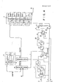
- Fig. 1 is a circuit diagram showing an embodiment of a digital muting circuit according to the present invention.
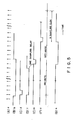
- a sampling clock a incoming to an input terminal 1 at a timing shown in Fig. 2 (A) in a model form is delivered to each clock terminal of D-type flip-flops 4 and 5 and a serial-to-parallel (S/P) converter 9, and to each clock terminal of an N-nary counter 10 and an N-bit register 16 which will be described later.
- This sampling clock a is incoming at a period equal to the transmission period of each word of a PCM sound data i having a number of quantized bits of N (N is an integer equal to 2 or more and e.g. N is 16) shown in Fig. 2(I).
- a mute control signal b shown in Fig. 2(B) from an external control circuit (not shown) is incoming to an input terminal 2 and is applied to a data input terminal of the D-type flip-flop 4.
- This mute control signal b is a binary signal which assumes low level at the time of on mute and high level at the time of off-mute.
- a mute release signal c which assumes low level only at the time of releasing the on-mute state as shown in Fig. 2(C), is incoming to an input terminal 3 from the above-mentioned external control circuit.
- the D-type flip-flops 4 and 5 form a circuit of two stages cascade-connected. From a Q output terminal of the D-type flip-flop 5, as shown in Fig. 2(E), a pulse e is taken out. The pulse e falls to low level at the second sampling clock after the mute control signal b fell to low level and arises to high level at the second sampling clock after the mute control signal b rose to high level.
- a NAND circuit 6 receives a output pulse of the D-type flip-flop 4 and the Q output pulse e of the flip-flop 5 to generate and output a pulse d as shown in Fig. 2(D).
- the D-type flip-flops 4 and 5 and the NAND circuit 6 constitute an on-mute control signal generating circuit 7.
- This circuit 7 generates and outputs from the NAND circuit 6 a negative polarity pulse d of one sampling clock period width synchronous with the sampling clock a in phase (i.e., one word transmission period of the input PCM sound data i) immediately after the mute control signal b shifted to low level to apply the negative polarity pulse d to a clear terminal of the N-nary counter 10 to clear this counter.
- the N-nary counter 10 is constituted so that its carry output is applied to its enable terminal through an inverter 11. This counter 10 outputs, from its carry output terminal a pulse f (shown in Fig.
- a D-type flip-flop 8 is constituted so that it is preset by the above-mentioned negative mute release signal c and is cleared for a time period during which the pulse e is at low level. As shown in Fig. 2(G), this flip-flop 8 generates a pulse g which shifts to low level at the time point when the pulse e has shifted to low level and shifts to high level at the time point when the mute release signal c is incoming after the pulse e shifted to high level to apply the pulse g to the clear terminal of the P/S converter 9.
- the S/P converter 9 Since the S/P converter 9 is cleared for a time period during which the above-mentioned pulse g is at low level, respective output signals of output terminals of N-bits are all at low level. Thus, at the time point when the first sampling clock a immediately after the pulse g shifted to high level is inputted, the S/P converter 9 produces a signal of high level from its output terminal labeled "1" to output it to the select terminal of a data selector 13 N as shown in Fig. 2(H). Further, at the time when the second sampling clock a is incoming, the S/P converter 9 produces a signal of high level from its output terminal labeled "2" to output it to the select terminal of a data selector 131 as shown in Fig. 2(H).
- the S/P converter 9 produces signals of high level in turn from the third to N-th terminals as shown in Fig. 2(H) to output them to select terminals of the data selectors 132 to 13 N-1 , respectively.
- the data selectors 131 to 13 N are circuits of the two-input, one-output type. Each selector is constituted so that when the input level of the select terminal is low, it selects and outputs the input data of the input terminal A, while when the input level of the select terminal is high, it selects and outputs the input data of the input terminal B.
- the reproduced PCM sound data i which has been reproduced from, e.g., a recording medium and then has been undergone all of de-interleaving, time axis compression, jitter absorption, and error detection and correction etc. is inputted through an input terminal 12 to respective input terminals B of the data selectors 131 to 13 N every corresponding bits.
- MSB of the PCM sound data is inputted to the input terminal B of the data selector 13 N and LSB of the PCM sound data is inputted to the input terminal B of the data selector 131.
- This PCM sound data have the number of quantized bits of N.
- Fig. 2 (I) in a model form they are inputted in the original order as indicated by the (M-3)th one word data ( M-3 D N to M-3 D1), the (M-2)th one word data ( M-2 D N to M-2 D1), the (M-1)th one word data ( M-1 D N to M-1 D1), the Mth one word data ( M D N to M D1) ...
- a D B in Fig. 2(I) and Figs. 3(A) to 3(C), which will be described later indicates the PCM sound data of the Bth bit of the Ath word.
- an explanation will be made on the assumption that the code form of the PCM sound data is offset binary.
- the data selector assembly has an arrangement such that a signal of high level H is always inputted to the input terminal A of the data selector 13 N among respective input terminal A of the data selectors 131 to 13 N , and that data obtained by applying polarity inversion to the output data of the data selector 13 N using the inverter 14 is delivered to each input terminal A of the other data selectors 131 to 13 N-1 .
- respective output data of the data selectors 13 N , 13 N-1 , ... 131 are outputted in a manner that data of MSB of input PCM sound data i, data of the (N-1)th bit thereof, ..., data of LSB thereof are selectively outputted during the off-mute period until the above-mentioned pulse g shifts to low level, as shown in Fig. 3(A) in a model form.
- this pulse g shifts to low level (this time point is indicated by GL at the upper portion of Fig. 3(A))
- all the outputs of N-bits of the S/P converter 9 shift to low level.
- the output data of the data selector 13 N shifts to high level (logical "1") which is the level of a signal incoming to its input terminal A. Further, respective output data of the data selectors 13 N-1 to 131 shift to low level (logical "0") which is the level of a signal obtained by applying polarity conversion to the output high level of the data selector 13 N using the inverter 14 which is incoming to each input terminal A of the data selectors 13 N-1 to 131.
- the value of the PCM sound data j of N-bits in total taken from the data selectors 13 N to 131 at the time of on-mute is indicated by "1000 ...0" as shown in Fig. 3(A).
- MSB which indicates the porality the PCM sound data assumes "1” and all the values of N-1 bits except for the former assume "0"
- the value of the PCM sound data j is held at this value during the on-mute period.
- This value represents "0" as well known in terms of offset binary, i.e., ground potential.
- the data selectors 13 N to 131 are switched so that the data selector 13 N first selects and outputs the input PCM sound data i of the input terminal B in sychronism with the sampling clock a. At times subsequent thereto, they are switched so as to select and output the input PCM sound data i in order of the data selectors 131, 132, ..., 13 N-1 every time the sampling clock a is incoming.
- the value of the PCM sound data j of N-bits in total taken from the data selectors 13 N to 131 changes as shown in Fig. 3(A).
- the value of the PCM sound data j assumes "1000 ...0" at the first time and then becomes equal to a value of N-bits in total comprising MSB which is the same value as the value P D N of MSB of the input PCM sound data i and remaining N-1 bits which are equal to the value P N of an inverted output of the MSB (this value indicates ground potential or an extremely small potential which is a value shifted on the negative side by a level corresponding to one quantization step with respect to the ground potential).
- An N-bit selector 15 is constructed so that when the above-mentioned pulse f is at low level, it selects and outputs the input data of the input terminal A, while when at high level, it selects and outputs the input data of the input terminal B.
- An N-bit register 16 stores and holds the parallel output PCM sound data of N-bits from the N-bit register 15 every time the sampling clock a is incoming and outputs the N-bit PCM sound data which have been stored when a preceding sampling clock is incoming, to a shift circuit 17 and to an output terminal 18.
- the shift circuit 17 outputs only MSB of the input N-bit data as MSB as it is, outputs data obtained by applying polarity inversion to the data of MSB of the input N-bit data as data of the second bit of higher order, and shifts bit by bit in a direction of lower order data of N-2 bits in total from the second bit of higher order to the second bit of lower order of the input N-bit data to output them to the input terminal A of the N-bit selector 15.
- the output signal of the N-bit register 16 becomes the PCM sound data l obtained by delaying the input PCM sound data i by one sampling clock as shown in Fig. 3(C) in a model form.
- the above-mentioned pulse f shifts to low level by the application of on-mute (the time point when this pulse f has just shifted to low level is indicated by FL at the upper portion of Fig.
- the PCM sound data i of one sampling clock immediately therebefore (indicated by M-1 D N , M-1 D N-1 , ..., M-1 D1 in Fig. 2(I)) is outputted from the N-bit register 16 as shown in Fig. 3(C).
- the input PCM sound data k of the input terminal A of the N-bit selector 15 is initiated to be outputted through the output terminal 18 with delay of one sampling clock period.
- the PCM sound data k is taken out from the shift circuit 17 as data of which value gradually decays by approximately -6 dB per each sampling clock.
- the PCM sound data k thus obtained is delivered to the input terminal A of the N-bit selector 15, and is then delivered to the N-bit register 16 via the N-bit selector 15.
- the output PCM sound data l of the N-bit register 16 becomes data obtained by delaying the PCM sound data k by one sampling clock period.
- the data thus obtained is then delivered to a D/A converter (not shown) via the output terminal 18.
- the output PCM sound data is not instantaneously muted to the minimum level, but gradually decays by approximately -6 dB per each sampling clock to reach the minimum level.
- this can prevent noise produced when muting is suddenly applied.
- the N-bit selector 15 is switched so as to output the input data of the input terminal B.
- the value "1000...0" of the PCM sound data j is taken out from the N-bit register 16.
- the N-bit register 16 begins outputting, as shown in Fig.
- the output of the S/P converter 9 shifts to high level in accordance with a predetermined sequence as previously described.
- the PCM sound data i at this time is initiated to be outputted as the output PCM sound data l from the N-bit register 16 with delay of one sampling clock period.
- the PCM sound data l during the duration T OFF varies in a manner that its level gradually returns from the minimum level to the level of the input PCM sound data i. According, even at the time of transition to the off- mute, the muting is not instantaneously released, but gradual returning to the ordinary level is conducted, thus making it possible to prevent occurrence of noise.
- FIG. 4 Another embodiment of a circuit according to the present invention will be now described with reference to Figs. 4 and 5.
- Fig. 4 components identical to those in Fig. 1 are respectively designated by like reference numerals and their explanation will be omitted.
- signals identical to those in Fig. 2 are respectively designated by like reference numerals and their explanation will be omitted.
- the output pulse f of the counter 19 is applied to the data input terminal of a D-type flip-flop 20 of a flip-flop circuit which comprises two stages of cascade-connected D-type flip-flops 20 and 21.
- a NAND circuit 22 performs not-logical-product of the Q output of the D-type flip-flop 20 and the Q output of the D-type flip-flop 21 to generate a negative polarity pulse m having one sampling clock width which falls at time point delayed by one sampling clock from the time point of the rise of the pulse f as shown in Fig. 5(E) to apply this pulse m to the clear terminal of the D-type flip-flop 8.
- the D-type flip-flop 8 produces as shown in Fig. 5(G) from the Q output terminal thereof a pulse n which falls at the incoming time point of the above-mentioned pulse m and rises at the incoming time point of the mute release signal c to apply this pulse n to the clear terminal of the S/P converter 9.
- the S/P converter outputs from its N-bit output terminals a pulse which shifts to high level in sequence for N sampling clock periods from the time point when the pulse n has shifted to high level.
- This embodiment provides a reciprocal arrangement of the input and output units in Fig. 3 by addition of the D-type flip-flops 20 and 21 and the NAND circuit 22.
- This embodiment can output the PCM sound data to which the mute processing has been implemented similar to that in the above-mentioned embodiment of Fig. 1 to the output terminal 18.
- the present invention is not limited to the above-mentioned embodiments, and hence the PCM sound data may have other code forms, e.g., twos complement notation etc.
- the inverter 14 and the inverter in the shift circuit 17 are removed, and inputs and the outputs thereof are directly coupled.
- the present invention can carry out on and off of muting with respect to the PCM sound data using a digital circuit configuration, thus making it possible to incorporate the muting circuit into ICs.
- the digital muting circuit implemented as IC has a greater resistance to change of power supply voltage, noise, temperature change, secular change and the like, and high reliability, and makes it possible to realize non-adjustment implementation, to reduce parts externally attached, and to be constructed at low cost and in a small size.
- this digital muting circuit is constituted so that level gradually changes immediately after on mute and immediately after off-mute, noise produced when suddenly changing the level can be prevented and thus on/off operation of muting natural from an aural point of view can be conducted.
Landscapes
- Engineering & Computer Science (AREA)
- Signal Processing (AREA)
- Signal Processing For Digital Recording And Reproducing (AREA)
- Analogue/Digital Conversion (AREA)
- Transmission Systems Not Characterized By The Medium Used For Transmission (AREA)
Applications Claiming Priority (2)
| Application Number | Priority Date | Filing Date | Title |
|---|---|---|---|
| JP61253678A JPS63108566A (ja) | 1986-10-27 | 1986-10-27 | デイジタルミユ−テイング回路 |
| JP253678/86 | 1986-10-27 |
Publications (3)
| Publication Number | Publication Date |
|---|---|
| EP0266159A2 true EP0266159A2 (de) | 1988-05-04 |
| EP0266159A3 EP0266159A3 (en) | 1989-11-08 |
| EP0266159B1 EP0266159B1 (de) | 1993-02-17 |
Family
ID=17254641
Family Applications (1)
| Application Number | Title | Priority Date | Filing Date |
|---|---|---|---|
| EP87309445A Expired - Lifetime EP0266159B1 (de) | 1986-10-27 | 1987-10-26 | Digitale Stummschaltung |
Country Status (5)
| Country | Link |
|---|---|
| US (1) | US4811370A (de) |
| EP (1) | EP0266159B1 (de) |
| JP (1) | JPS63108566A (de) |
| KR (1) | KR910006154B1 (de) |
| DE (1) | DE3784212T2 (de) |
Cited By (3)
| Publication number | Priority date | Publication date | Assignee | Title |
|---|---|---|---|---|
| GB2222331A (en) * | 1988-08-23 | 1990-02-28 | Samsung Electronics Co Ltd | A muting circuit for use in a digital audio system |
| EP0514041A3 (en) * | 1991-05-02 | 1993-12-15 | Texas Instruments Ltd | Digital data decoder using error information for selecting one of a plurality of transmissions |
| KR100499481B1 (ko) * | 2002-11-09 | 2005-07-07 | 엘지전자 주식회사 | 디지털 오디오의 음량 자동 조절 장치 및 방법 |
Families Citing this family (5)
| Publication number | Priority date | Publication date | Assignee | Title |
|---|---|---|---|---|
| JPH08321132A (ja) * | 1995-05-26 | 1996-12-03 | Canon Inc | 記録再生装置 |
| US5918205A (en) * | 1996-01-30 | 1999-06-29 | Lsi Logic Corporation | Audio decoder employing error concealment technique |
| US5920833A (en) * | 1996-01-30 | 1999-07-06 | Lsi Logic Corporation | Audio decoder employing method and apparatus for soft-muting a compressed audio signal |
| US6405092B1 (en) * | 1997-09-29 | 2002-06-11 | William Vincent Oxford | Method and apparatus for amplifying and attenuating digital audio |
| US7337026B2 (en) * | 2004-03-19 | 2008-02-26 | Via Technologies Inc. | Digital audio volume control |
Family Cites Families (7)
| Publication number | Priority date | Publication date | Assignee | Title |
|---|---|---|---|---|
| JPS5542384A (en) * | 1978-09-21 | 1980-03-25 | Mitsubishi Electric Corp | Pcm sound reproducer |
| US4291405A (en) * | 1979-09-07 | 1981-09-22 | Bell Telephone Laboratories, Incorporated | Error reduction speech communication system |
| DE3034756C2 (de) * | 1979-09-18 | 1986-09-04 | Victor Company Of Japan, Ltd., Yokohama, Kanagawa | Audiosignalverarbeitungseinrichtung |
| US4430742A (en) * | 1981-11-20 | 1984-02-07 | Motorola, Inc. | Data muting method and apparatus for radio communications systems |
| JPH0619904B2 (ja) * | 1983-05-20 | 1994-03-16 | 日本ビクター株式会社 | デジタル信号の波形処理方式 |
| JPH0770177B2 (ja) * | 1984-01-25 | 1995-07-31 | 株式会社日立製作所 | ディジタル信号再生装置 |
| JPH0777331B2 (ja) * | 1986-08-12 | 1995-08-16 | ソニー株式会社 | デジタルオ−デイオ信号の減衰装置 |
-
1986
- 1986-10-27 JP JP61253678A patent/JPS63108566A/ja active Granted
-
1987
- 1987-10-26 US US07/112,489 patent/US4811370A/en not_active Expired - Fee Related
- 1987-10-26 DE DE8787309445T patent/DE3784212T2/de not_active Expired - Fee Related
- 1987-10-26 EP EP87309445A patent/EP0266159B1/de not_active Expired - Lifetime
- 1987-10-26 KR KR1019870011862A patent/KR910006154B1/ko not_active Expired
Cited By (5)
| Publication number | Priority date | Publication date | Assignee | Title |
|---|---|---|---|---|
| GB2222331A (en) * | 1988-08-23 | 1990-02-28 | Samsung Electronics Co Ltd | A muting circuit for use in a digital audio system |
| DE3927377A1 (de) * | 1988-08-23 | 1990-03-08 | Samsung Electronics Co Ltd | Rauschsperrenschaltkreis in einem digitalen tonsystem |
| GB2222331B (en) * | 1988-08-23 | 1993-05-19 | Samsung Electronics Co Ltd | A muting circuit for use in a digital audio system |
| EP0514041A3 (en) * | 1991-05-02 | 1993-12-15 | Texas Instruments Ltd | Digital data decoder using error information for selecting one of a plurality of transmissions |
| KR100499481B1 (ko) * | 2002-11-09 | 2005-07-07 | 엘지전자 주식회사 | 디지털 오디오의 음량 자동 조절 장치 및 방법 |
Also Published As
| Publication number | Publication date |
|---|---|
| JPH0578104B2 (de) | 1993-10-28 |
| DE3784212T2 (de) | 1993-08-05 |
| KR910006154B1 (ko) | 1991-08-16 |
| US4811370A (en) | 1989-03-07 |
| JPS63108566A (ja) | 1988-05-13 |
| EP0266159B1 (de) | 1993-02-17 |
| KR880005603A (ko) | 1988-06-29 |
| DE3784212D1 (de) | 1993-03-25 |
| EP0266159A3 (en) | 1989-11-08 |
Similar Documents
| Publication | Publication Date | Title |
|---|---|---|
| JP2573850B2 (ja) | アナログ−デイジタル変換装置 | |
| JPH0631989B2 (ja) | 電子楽器の波形発生装置 | |
| US4811370A (en) | Digital muting circuit | |
| US4584701A (en) | Reverberator having tapped and recirculating delay lines | |
| KR950012379B1 (ko) | 직렬 비트 디지털 신호 처리 장치 | |
| JPS5927347A (ja) | 到来信号の所望の関数を発生する関数発生器 | |
| US5576709A (en) | Delay circuit using a digital memory | |
| CA1210517A (en) | Broadband transmission on limited bandwidth digital line | |
| GB2095952A (en) | Bi-phase space code data signal reproducing circuit | |
| US5329484A (en) | Semiconductor memory circuit, semiconductor memory module using the same, and acoustic signal reproducing system | |
| KR100196477B1 (ko) | A/d 변환기 | |
| JP2762941B2 (ja) | 背景雑音発生装置 | |
| US5357248A (en) | Sampling rate converter | |
| US4549305A (en) | Adaptive differential PCM decoder | |
| US4805508A (en) | Sound synthesizing circuit | |
| FI92778C (fi) | Digitaalisignaalin amplitudinsäätöjärjestelmä digitaalisignaalien muuttamiseksi jokseenkin tasaisin dB-askelin | |
| JP2989431B2 (ja) | 遅延回路 | |
| JPS602688B2 (ja) | デイジタル信号減衰器 | |
| JP2698843B2 (ja) | 電子楽器 | |
| JP3041932B2 (ja) | サンプルレート変換回路 | |
| KR920000407Y1 (ko) | Dat시스템에서의 샘플링 데이타 변환회로 | |
| JPH07123214B2 (ja) | D/a変換装置 | |
| JPH06188685A (ja) | Firフィルタ | |
| JPH0339415B2 (de) | ||
| JPS59172104A (ja) | デイジタル・デ−タ・エンベロ−プ・コントロ−ル回路 |
Legal Events
| Date | Code | Title | Description |
|---|---|---|---|
| PUAI | Public reference made under article 153(3) epc to a published international application that has entered the european phase |
Free format text: ORIGINAL CODE: 0009012 |
|
| AK | Designated contracting states |
Kind code of ref document: A2 Designated state(s): DE FR GB |
|
| PUAL | Search report despatched |
Free format text: ORIGINAL CODE: 0009013 |
|
| AK | Designated contracting states |
Kind code of ref document: A3 Designated state(s): DE FR GB |
|
| 17P | Request for examination filed |
Effective date: 19891208 |
|
| 17Q | First examination report despatched |
Effective date: 19911125 |
|
| GRAA | (expected) grant |
Free format text: ORIGINAL CODE: 0009210 |
|
| AK | Designated contracting states |
Kind code of ref document: B1 Designated state(s): DE FR GB |
|
| REF | Corresponds to: |
Ref document number: 3784212 Country of ref document: DE Date of ref document: 19930325 |
|
| ET | Fr: translation filed | ||
| PLBE | No opposition filed within time limit |
Free format text: ORIGINAL CODE: 0009261 |
|
| STAA | Information on the status of an ep patent application or granted ep patent |
Free format text: STATUS: NO OPPOSITION FILED WITHIN TIME LIMIT |
|
| 26N | No opposition filed | ||
| PGFP | Annual fee paid to national office [announced via postgrant information from national office to epo] |
Ref country code: FR Payment date: 19951010 Year of fee payment: 9 |
|
| PGFP | Annual fee paid to national office [announced via postgrant information from national office to epo] |
Ref country code: GB Payment date: 19951017 Year of fee payment: 9 |
|
| PGFP | Annual fee paid to national office [announced via postgrant information from national office to epo] |
Ref country code: DE Payment date: 19951026 Year of fee payment: 9 |
|
| PG25 | Lapsed in a contracting state [announced via postgrant information from national office to epo] |
Ref country code: GB Effective date: 19961026 |
|
| GBPC | Gb: european patent ceased through non-payment of renewal fee |
Effective date: 19961026 |
|
| PG25 | Lapsed in a contracting state [announced via postgrant information from national office to epo] |
Ref country code: FR Effective date: 19970630 |
|
| PG25 | Lapsed in a contracting state [announced via postgrant information from national office to epo] |
Ref country code: DE Effective date: 19970701 |
|
| REG | Reference to a national code |
Ref country code: FR Ref legal event code: ST |