EP0265090B1 - Method for making multisensor piezoelectric elements - Google Patents
Method for making multisensor piezoelectric elements Download PDFInfo
- Publication number
- EP0265090B1 EP0265090B1 EP87308529A EP87308529A EP0265090B1 EP 0265090 B1 EP0265090 B1 EP 0265090B1 EP 87308529 A EP87308529 A EP 87308529A EP 87308529 A EP87308529 A EP 87308529A EP 0265090 B1 EP0265090 B1 EP 0265090B1
- Authority
- EP
- European Patent Office
- Prior art keywords
- gold
- piezoelectric
- germanium
- layers
- films
- Prior art date
- Legal status (The legal status is an assumption and is not a legal conclusion. Google has not performed a legal analysis and makes no representation as to the accuracy of the status listed.)
- Expired - Lifetime
Links
- 238000000034 method Methods 0.000 title claims description 22
- BYDQGSVXQDOSJJ-UHFFFAOYSA-N [Ge].[Au] Chemical compound [Ge].[Au] BYDQGSVXQDOSJJ-UHFFFAOYSA-N 0.000 claims description 36
- 238000000151 deposition Methods 0.000 claims description 10
- 238000010438 heat treatment Methods 0.000 claims description 7
- 238000004544 sputter deposition Methods 0.000 claims description 7
- 238000005452 bending Methods 0.000 claims description 6
- 238000002844 melting Methods 0.000 claims 3
- 230000008018 melting Effects 0.000 claims 3
- 239000000463 material Substances 0.000 description 23
- 229910045601 alloy Inorganic materials 0.000 description 18
- 239000000956 alloy Substances 0.000 description 18
- PCHJSUWPFVWCPO-UHFFFAOYSA-N gold Chemical group [Au] PCHJSUWPFVWCPO-UHFFFAOYSA-N 0.000 description 10
- 229910052737 gold Inorganic materials 0.000 description 8
- 239000010931 gold Substances 0.000 description 8
- 230000005496 eutectics Effects 0.000 description 5
- 239000004593 Epoxy Substances 0.000 description 4
- 239000011888 foil Substances 0.000 description 4
- 229910052732 germanium Inorganic materials 0.000 description 4
- GNPVGFCGXDBREM-UHFFFAOYSA-N germanium atom Chemical compound [Ge] GNPVGFCGXDBREM-UHFFFAOYSA-N 0.000 description 4
- 230000010287 polarization Effects 0.000 description 4
- 239000000758 substrate Substances 0.000 description 4
- 230000008859 change Effects 0.000 description 3
- 238000005304 joining Methods 0.000 description 3
- 238000005259 measurement Methods 0.000 description 3
- 230000035945 sensitivity Effects 0.000 description 3
- PXHVJJICTQNCMI-UHFFFAOYSA-N Nickel Chemical compound [Ni] PXHVJJICTQNCMI-UHFFFAOYSA-N 0.000 description 2
- BQCADISMDOOEFD-UHFFFAOYSA-N Silver Chemical compound [Ag] BQCADISMDOOEFD-UHFFFAOYSA-N 0.000 description 2
- 238000006664 bond formation reaction Methods 0.000 description 2
- 230000006835 compression Effects 0.000 description 2
- 238000007906 compression Methods 0.000 description 2
- 239000004020 conductor Substances 0.000 description 2
- 229910052709 silver Inorganic materials 0.000 description 2
- 239000004332 silver Substances 0.000 description 2
- 235000012431 wafers Nutrition 0.000 description 2
- 229910000497 Amalgam Inorganic materials 0.000 description 1
- 229910001369 Brass Inorganic materials 0.000 description 1
- RYGMFSIKBFXOCR-UHFFFAOYSA-N Copper Chemical group [Cu] RYGMFSIKBFXOCR-UHFFFAOYSA-N 0.000 description 1
- 230000001133 acceleration Effects 0.000 description 1
- 238000004026 adhesive bonding Methods 0.000 description 1
- 238000013459 approach Methods 0.000 description 1
- 239000010951 brass Substances 0.000 description 1
- 239000004568 cement Substances 0.000 description 1
- 239000000919 ceramic Substances 0.000 description 1
- 239000003795 chemical substances by application Substances 0.000 description 1
- 238000001816 cooling Methods 0.000 description 1
- 229910052802 copper Inorganic materials 0.000 description 1
- 239000010949 copper Substances 0.000 description 1
- 230000008021 deposition Effects 0.000 description 1
- 238000001514 detection method Methods 0.000 description 1
- 238000009792 diffusion process Methods 0.000 description 1
- 230000000694 effects Effects 0.000 description 1
- 229920006333 epoxy cement Polymers 0.000 description 1
- 238000010304 firing Methods 0.000 description 1
- 239000011521 glass Substances 0.000 description 1
- 239000007788 liquid Substances 0.000 description 1
- 238000004519 manufacturing process Methods 0.000 description 1
- QSHDDOUJBYECFT-UHFFFAOYSA-N mercury Chemical compound [Hg] QSHDDOUJBYECFT-UHFFFAOYSA-N 0.000 description 1
- 229910052753 mercury Inorganic materials 0.000 description 1
- CBBVHSHLSCZIHD-UHFFFAOYSA-N mercury silver Chemical compound [Ag].[Hg] CBBVHSHLSCZIHD-UHFFFAOYSA-N 0.000 description 1
- 229910052751 metal Inorganic materials 0.000 description 1
- 239000002184 metal Substances 0.000 description 1
- 239000007769 metal material Substances 0.000 description 1
- 230000005012 migration Effects 0.000 description 1
- 238000013508 migration Methods 0.000 description 1
- 239000000203 mixture Substances 0.000 description 1
- 238000012986 modification Methods 0.000 description 1
- 230000004048 modification Effects 0.000 description 1
- 229910052759 nickel Inorganic materials 0.000 description 1
- 238000003825 pressing Methods 0.000 description 1
- 230000008569 process Effects 0.000 description 1
- 229910052594 sapphire Inorganic materials 0.000 description 1
- 239000010980 sapphire Substances 0.000 description 1
- 229910000679 solder Inorganic materials 0.000 description 1
- 239000007787 solid Substances 0.000 description 1
- 238000006467 substitution reaction Methods 0.000 description 1
- 229910052715 tantalum Inorganic materials 0.000 description 1
- GUVRBAGPIYLISA-UHFFFAOYSA-N tantalum atom Chemical compound [Ta] GUVRBAGPIYLISA-UHFFFAOYSA-N 0.000 description 1
- WFKWXMTUELFFGS-UHFFFAOYSA-N tungsten Chemical compound [W] WFKWXMTUELFFGS-UHFFFAOYSA-N 0.000 description 1
- 229910052721 tungsten Inorganic materials 0.000 description 1
- 239000010937 tungsten Substances 0.000 description 1
- 239000013598 vector Substances 0.000 description 1
- 235000012773 waffles Nutrition 0.000 description 1
Images

Classifications
-
- G—PHYSICS
- G01—MEASURING; TESTING
- G01L—MEASURING FORCE, STRESS, TORQUE, WORK, MECHANICAL POWER, MECHANICAL EFFICIENCY, OR FLUID PRESSURE
- G01L1/00—Measuring force or stress, in general
- G01L1/16—Measuring force or stress, in general using properties of piezoelectric devices
-
- H—ELECTRICITY
- H10—SEMICONDUCTOR DEVICES; ELECTRIC SOLID-STATE DEVICES NOT OTHERWISE PROVIDED FOR
- H10N—ELECTRIC SOLID-STATE DEVICES NOT OTHERWISE PROVIDED FOR
- H10N30/00—Piezoelectric or electrostrictive devices
- H10N30/01—Manufacture or treatment
- H10N30/06—Forming electrodes or interconnections, e.g. leads or terminals
-
- H—ELECTRICITY
- H10—SEMICONDUCTOR DEVICES; ELECTRIC SOLID-STATE DEVICES NOT OTHERWISE PROVIDED FOR
- H10N—ELECTRIC SOLID-STATE DEVICES NOT OTHERWISE PROVIDED FOR
- H10N30/00—Piezoelectric or electrostrictive devices
- H10N30/30—Piezoelectric or electrostrictive devices with mechanical input and electrical output, e.g. functioning as generators or sensors
- H10N30/302—Sensors
-
- Y—GENERAL TAGGING OF NEW TECHNOLOGICAL DEVELOPMENTS; GENERAL TAGGING OF CROSS-SECTIONAL TECHNOLOGIES SPANNING OVER SEVERAL SECTIONS OF THE IPC; TECHNICAL SUBJECTS COVERED BY FORMER USPC CROSS-REFERENCE ART COLLECTIONS [XRACs] AND DIGESTS
- Y10—TECHNICAL SUBJECTS COVERED BY FORMER USPC
- Y10T—TECHNICAL SUBJECTS COVERED BY FORMER US CLASSIFICATION
- Y10T29/00—Metal working
- Y10T29/42—Piezoelectric device making
Definitions
- the present invention relates to a method for making devices for sensing elastic changes, and more particularly to piezoelectric elements for sensing dynamic bending moments in these sensing elements.
- One use for such a device is for detection and measurement of Coriolis accelerations in a multisensor rate gyro.
- the preferred configuration for the piezoelectric elements is in the form of a "piezo-pair" which consists of two layers of piezoelectric materials bonded together.
- the piezoelectric material is polarized in such a manner that, were axial stress applied thereto, a voltage would appear between the faces of the layers.
- an epoxy with a conducting material mixed in is used to cement the piezoelectric layers together.
- bias stresses are not harmful since they appear only as a temperature induced scale factor change that could be compensated.
- the temperature induced stresses would relax with time, thereby producing a scale factor/temperature change hysteresis which is prohibitively large.
- Noren describes a piezo-pair bond formation which is extremely complicated.
- the Noren piezo-pair bond is formed when the waffle shaped gold foil forms a flexible gold film bonded to the copper interfaces.
- the Noren process requires 650°C, 30 minutes and 5.5 x 10⁵ Nm ⁇ 2 above atmospheric pressure (80 PSI) applied per face. Since vacuum conditions do not exist during the bond formation, the Noren bond could be weak, and trapped gas could exist at the joint formed by the gold foil.
- IBM Technical Disclosure Bulletin, Volume 21, No. 7, Dec. 1978, page 2986 discloses a technique for bonding a piezoelectric member to a substrate.
- the substrate is provided with an electrically conductive surface on one face
- the piezoelectric member is provided with an electrically conductive surface on each face.
- the piezoelectric member is bonded to the substrate by placing the former on the latter and subjecting the combination to a load so as to bring the piezoelectric member and substrate into intimate contact.
- the piezoelectric device is activated by a suitable potential applied between the electrically conductive surfaces on the respective faces so that mechanical energy generated in the piezoelectric device is transferred to the interface and released as heat thereby bonding the piezoelectric material to the base member.
- U.S. 4078711 there is disclosed a method for attaching a silicon-on-sapphire device to a gold-plated surface.
- a gold layer is deposited on a layer of tungsten which is itself deposited on the device, and gold-germanium, being an alloy compatible with gold, is interposed between the two gold layers and heated so as to produce a bond.
- a metallic material such as gold-germanium (Au-Ge) is first deposited onto the opposed surfaces of the piezoelectric layers which are to be bonded.
- the layers are heated sufficiently to fuse the Au-Ge material so that the piezoelectric layers are bonded to form a piezo-pair.
- the piezo-pair is poled.
- the edges of the ceramic layers are chamfered prior to the sputtering operation. This results in a piezo-pair having a V shaped electrode contact at the center metallic layer.
- the present invention as disclosed below not only provides a method of making a sensing piezoelectric element which is impervious to any bias stresses caused by changes in temperature, but also a simple method for fabricating piezo-pair elements for detecting changes in stress in a multisensor.
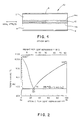
- FIG. 1 there is shown a conventional piezo-pair sensor having two layers of piezoelectric material 2 and 4 of approximately .024 inches (0.61 mm) thick. Coated on the outer surfaces of respective layers 2 and 4 are corresponding electrodes 6 and 8. These electrodes, which may be made up of silver, nickel, or gold for example cover all or part of the length of piezo-pair sensor 10. Piezoelectric layers 2 and 4 are bound to a center foil thereof by means of epoxy layers 14a and 14b. Center foil 12 is approximately .003 millimeters thick and can be made from a number of materials such as brass or tantalum, to name a few.
- center foil 12 and piezoelectric layers 2 and 4 have different coefficients of expansion, and therefore do not expand at the same rate.
- axial stresses between center foil 12 and piezoelectric layers 2 and 4 show up as shears in epoxy cement layers 14a and 14b, respectively.
- a presence of the axial stresses modifies the sensitivity of the piezo-pair sensor as a signal generator.
- the epoxy layers do flow with time, so as to relieve the stresses locked therein, "creep" results in the piezo-pair sensor.
- the method of bonding the two piezoelectric layers with this material must take into consideration the fact that the bonding temperature must be greater than the operating and poling temperature of a piezo-pair sensor thus formed, and less than the firing temperature for creating the piezoelectric layers.
- the Au-Ge alloy which has 12 weight percent germanium, [Au-12 w/o Ge] could be used for bonding the two piezoelectric layers to form a piezo-pair sensor.
- this Au-Ge alloy has a eutectic temperature 16 which is 356°C.
- a eutectic temperature is low enough so that it does not approach the temperature whereby the characteristics of the piezoelectric layers would be changed and yet high enough so that it is sufficiently above the operating temperature of a sensor made from piezoelectric elements bonded by such an alloy, and sufficiently above the poling temperature of the piezoelectric element.
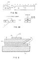
- [Au-Ge] film 22 is sputtered by the aforesaid Au-Ge alloy target of the same stoichiometry. For the ease of connecting an electrical contact to inner surface 18I, an edge of the same is chamfered at point 20. The reason sputtering is used to deposit the Au-Ge alloy onto inner surface 18I is that the depth of the deposition and the stoichiometry of the alloy can be precisely controlled. Needless to say, the thickness of Au-Ge film 22 is drawn for illustration purposes only and it may in fact have a thickness of less than 25,000 Angstroms.
- piezoelectric layer 18 After piezoelectric layer 18 has been sputtered with Au-Ge film 22, it is combined with a corresponding piezoelectric layer 18a, which also has sputtered thereon at its inner surface 181a a film 22a of Au-Ge alloy.
- element 18a is shown rotated over and in proximity with element 18; and a small pressure P is applied to expedite the bonding.
- the fused part then provides an internally chamfered edge which is electrically conducting and integral with the conducting layer which now forms the center electrode of the resultant piezo-pair.
- the chamfered notch is useful for the attachment of the wire lead. See also Figure 4a.
- film 22 also has an outer surface 22I chamfered at position 24.
- film 22a of the second wafer is placed on top of the corresponding surface 22I with chamfered edges 24 and 24a in alignment.
- a combination of layers 18 and 18a and films 22 and 22a, hereinafter designated as piezo-pair 26, is then heated at an elevated temperature so that the respective Au-Ge films on corresponding outer surfaces 22I and 22Ia can fuse, thereby bonding piezoelectric layer 18 intimately to the corresponding piezoelectric layer 18a. See Figure 3b.
- the temperature which is needed to cause the two Au-Ge alloy films to fuse is the eutectic temperature of the same. It should be appreciated that were a different composition or a chemically different alloy which contains all the criteria mentioned hereinabove used, the eutectic temperature, i.e., the temperature which is needed to fuse the alloy films for bonding the two piezoelectric layers, would of course be different.
- piezo-pair 26 After piezo-pair 26 has been heated at the Au-Ge alloy eutectic temperature for a specific length of time, it becomes "creep-free", as films 22 and 22a are bonded together to form a one piece piezo-pair. Hence, regardless of how much stress is applied thereto, there will not be any "creep" between film 22, 22a and the piezoelectric layers, 18 and 18a. Too, it should be appreciated that since the dimension of alloy film 22, 22a is extremely thin, stress experienced by layers 18 and 18a and film 22, 22a is minimal.
- a present invention method further includes the depositing of metallic conductor layers 30 and 32 on respective outer surfaces 18o and 18oa of corresponding layers 18 and 18a.
- a small pressure such as 3.4 x 10⁴ Nm ⁇ 2 above atmospheric pressure (5 PSI) may be applied.
- a 'V' notch 34 is formed from the aligned chamfered edges 24 and 24a. Note that notch 34 is necessitated by the fact that in a real world setting, because the dimension of alloy film 28 is extremely thin, a place must be provided somewhere on piezo-pair 26 for the attachment of an electrode to alloy film 28.
- an electrode 36 is connected to alloy film 28 by means of solder 38. It is via electrode 36 that signals corresponding to stress applied to piezo-pair 26 are obtained.
- the poling and sensing of the piezo-pair element is discussed hereinbelow.
- piezoelectric materials require that the sensor constructed therefrom be poled in order to be activated.
- Such poling is conventionally accomplished by heating the material to a temperature which is both high enough to permit poling and sufficiently above the device operating temperature to prevent depoling during operation.
- a high voltage is applied between the electrodes while at the elevated temperature to cause the dipole moments of the piezoelectric material to align parallel to the arrows 40 and 42 of Figure 4a.
- the poling polarity shown in Figure 4a if a bending moment is applied to the piezo-pair 26 about axis 44, one layer (18 for example) would be in tension and the other layer (18a for example) would be in compression.
- the sensor measures bending moments applied to the beam about axis 44. These bending moments apply a tension in one layer and a compression in the other layer.
- the layers are poled with polarization vectors 40 and 42 aligned antiparallel or parallel to each other. Polarization of the layers in the antiparallel direction requires that a voltage be applied between the center electrode and between the outer electrodes connected in parallel. Polarization of the layers in the parallel direction requires that a voltage be applied only between the outer electrodes. Sensing the output of the antiparallel polarized piezo-pair requires that the signal be measured between the outer electrodes.
- Sensing of the output of the parallel polarized piezo-pair requires that the signal be measured between the center electrode and between the outer electrodes connected in parallel. In either polarization case, it is necessary that an electrical connection to the center electrode be readily achieved. This electrical connection is facilitated by the "V" notch which results when the chamfered surface of these two wafers are combined into the piezo-pair of Figure 4b since the center electrode is continuous along the surface of the "V".
- piezo-pair 26 in effect is a unitary sensor, it is substantially impervious to "creep", thereby the measurements which the detector obtains from alloy film 28 are much more accurate and are devoid of distortions.
- Figure 4b shows. a perspective view of the piezo-pair sensor shown in Figure 4a.
- Another embodiment of this invention allows a piezoelectric layer to be bonded to materials other than another piezoelectric.
- a non-piezoelectric material layer 51 is bonded to a piezoelectric material layer 55.
- the bonding of piezoelectric material 55 to non-piezoelectric layer 51 requires that the non-piezoelectric layer be compatible (in terms of bonding) with gold/germanium layer 54.
- gold/germanium layer 54 is not compatible with non-piezoelectric layer 51, a suitable interface layer such as 52 needs to be deposited on non-piezoelectric layer 51.
- a gold/germanium layer 53 is then sputtered onto interface layer 52, and piezoelectric material layer 55 is joined to non-piezoelectric material layer 51 in a manner similar to that described hereinabove for the piezo-pair configuration.
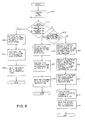
- Fig. 6 illustrates the steps for forming the different embodiments of the instant invention.
- the layers are chamfered for each of the embodiments.
- a determination is made as to whether the layers are both piezoelectric or are piezoelectric and non-piezoelectric, per block 601. If the layers are in fact both piezoelectric layers, then via route A, gold-germanium films are deposited on the opposed surfaces of the layers by sputtering, per block 602.
- the layers are positioned so as to form an assembly of layers and films. And the assembly is heated at an elevated temperature, per block 604.
- the layers, as determined in block 601 are found to be comprised of a piezoelectric and non-piezoelectric layer, then a next determination via route B, per block 605, as to whether these layers are compatible with gold-germanium is taken. If they are compatible, then gold-germanium films are deposited onto opposed surfaces of the layers by sputtering, per block 606. Next, these layers are positioned to form an assembly of layers and films per block 607. After which, the assembly is heated at an elevated temperature, per block 608.
- a bonding compatible film has to be deposited onto the surface of the incompatible layer so as to form a resultant surface, per block 609.
- gold-germanium films are deposited onto the resultant surface and the surface of the compatible layer, respectively, if only one of the layers is incompatible with gold-germanium, as shown in block 610. If both layers are incompatible with gold-germanium, the gold-germanium films are deposited onto the respective resultant surfaces, per block 611. Thereafter, like the previous embodiments, the layers are positioned to form an assembly of layers and films; and the assembly is then heated at an elevated temperature, per block 612 and 613, respectively.
Landscapes
- Physics & Mathematics (AREA)
- General Physics & Mathematics (AREA)
- Engineering & Computer Science (AREA)
- Manufacturing & Machinery (AREA)
- Gyroscopes (AREA)
- Measuring Fluid Pressure (AREA)
- Transmission And Conversion Of Sensor Element Output (AREA)
- Force Measurement Appropriate To Specific Purposes (AREA)
- Measurement Of Length, Angles, Or The Like Using Electric Or Magnetic Means (AREA)
Applications Claiming Priority (2)
| Application Number | Priority Date | Filing Date | Title |
|---|---|---|---|
| US06/921,520 US4769882A (en) | 1986-10-22 | 1986-10-22 | Method for making piezoelectric sensing elements with gold-germanium bonding layers |
| US921520 | 1997-09-02 |
Publications (3)
| Publication Number | Publication Date |
|---|---|
| EP0265090A2 EP0265090A2 (en) | 1988-04-27 |
| EP0265090A3 EP0265090A3 (en) | 1988-09-21 |
| EP0265090B1 true EP0265090B1 (en) | 1991-07-31 |
Family
ID=25445555
Family Applications (1)
| Application Number | Title | Priority Date | Filing Date |
|---|---|---|---|
| EP87308529A Expired - Lifetime EP0265090B1 (en) | 1986-10-22 | 1987-09-25 | Method for making multisensor piezoelectric elements |
Country Status (8)
| Country | Link |
|---|---|
| US (1) | US4769882A (cg-RX-API-DMAC7.html) |
| EP (1) | EP0265090B1 (cg-RX-API-DMAC7.html) |
| JP (1) | JPS63190391A (cg-RX-API-DMAC7.html) |
| AU (1) | AU595071B2 (cg-RX-API-DMAC7.html) |
| CA (1) | CA1317478C (cg-RX-API-DMAC7.html) |
| DE (1) | DE3771831D1 (cg-RX-API-DMAC7.html) |
| IL (1) | IL83901A (cg-RX-API-DMAC7.html) |
| NO (1) | NO178317C (cg-RX-API-DMAC7.html) |
Families Citing this family (21)
| Publication number | Priority date | Publication date | Assignee | Title |
|---|---|---|---|---|
| SU1642962A3 (ru) * | 1989-06-16 | 1991-04-15 | Е.И.Новиков | Пьезочастотный датчик силы |
| JP3039971B2 (ja) * | 1989-09-19 | 2000-05-08 | 株式会社日立製作所 | 接合型圧電装置及び製造方法並びに接合型圧電素子 |
| FR2693795B1 (fr) * | 1992-07-15 | 1994-08-19 | Commissariat Energie Atomique | Jauge de contrainte sur support souple et capteur muni de ladite jauge. |
| US6484585B1 (en) | 1995-02-28 | 2002-11-26 | Rosemount Inc. | Pressure sensor for a pressure transmitter |
| US5755909A (en) * | 1996-06-26 | 1998-05-26 | Spectra, Inc. | Electroding of ceramic piezoelectric transducers |
| US6164140A (en) * | 1998-10-09 | 2000-12-26 | Kalinoski; Richard W. | Solid state transducer for Coriolis flowmeter |
| US6505516B1 (en) | 2000-01-06 | 2003-01-14 | Rosemount Inc. | Capacitive pressure sensing with moving dielectric |
| US6561038B2 (en) | 2000-01-06 | 2003-05-13 | Rosemount Inc. | Sensor with fluid isolation barrier |
| US6520020B1 (en) | 2000-01-06 | 2003-02-18 | Rosemount Inc. | Method and apparatus for a direct bonded isolated pressure sensor |
| AU2629901A (en) | 2000-01-06 | 2001-07-16 | Rosemount Inc. | Grain growth of electrical interconnection for microelectromechanical systems (mems) |
| US6508129B1 (en) | 2000-01-06 | 2003-01-21 | Rosemount Inc. | Pressure sensor capsule with improved isolation |
| JP2002144239A (ja) * | 2000-11-08 | 2002-05-21 | Alps Engineering:Kk | ノズル |
| US6672168B2 (en) | 2001-09-24 | 2004-01-06 | Andrew Braugh | Multi-level machine vibration tester marker pen |
| US6848316B2 (en) | 2002-05-08 | 2005-02-01 | Rosemount Inc. | Pressure sensor assembly |
| AU2002339750A1 (en) * | 2002-08-30 | 2004-03-29 | Usc Corporation | Piezoelectric generator |
| WO2005026678A1 (de) * | 2003-09-17 | 2005-03-24 | Kistler Holding Ag | Mehrschichtiges piezoelektrisches messelement und ein druck- oder kraftsensor umfassend ein solches messelement |
| JP3866258B2 (ja) * | 2004-08-24 | 2007-01-10 | 太平洋セメント株式会社 | 圧電デバイスおよびこれを備える圧電スイッチ |
| JP2009534651A (ja) * | 2006-04-20 | 2009-09-24 | ヴェクトロン インターナショナル,インク | 高圧環境用の電気音響センサ |
| WO2011035147A2 (en) * | 2009-09-18 | 2011-03-24 | Delaware Capital Formation, Inc. | Controlled compressional wave components of thickness shear mode multi-measurand sensors |
| WO2020194026A1 (en) * | 2019-03-23 | 2020-10-01 | Secretary, Department Of Atomic Energy | Diffusion bonding of piezoelectric crystal to metal wear plate |
| CN110379916B (zh) * | 2019-07-05 | 2020-10-27 | 中国科学院物理研究所 | 压电陶瓷元件的制备方法 |
Family Cites Families (12)
| Publication number | Priority date | Publication date | Assignee | Title |
|---|---|---|---|---|
| US2709147A (en) * | 1951-09-12 | 1955-05-24 | Bell Telephone Labor Inc | Methods for bonding silica bodies |
| US3179826A (en) * | 1961-09-14 | 1965-04-20 | Trott Winfield James | Piezolelectric assembly |
| AT237930B (de) * | 1962-09-12 | 1965-01-11 | Hans Dipl Ing Dr Techn List | Piezoelektrische Einrichtung, insbesondere zur Kraftmessung, und Verfahren zu ihrer Herstellung |
| US3590467A (en) * | 1968-11-15 | 1971-07-06 | Corning Glass Works | Method for bonding a crystal to a solid delay medium |
| FR2182295A5 (cg-RX-API-DMAC7.html) * | 1972-04-25 | 1973-12-07 | Thomson Csf | |
| US3897628A (en) * | 1973-11-19 | 1975-08-05 | Rca Corp | Method of forming a thin piezoelectric body metallically bonded to a propagation medium crystal |
| US3986251A (en) * | 1974-10-03 | 1976-10-19 | Motorola, Inc. | Germanium doped light emitting diode bonding process |
| US4042951A (en) * | 1975-09-25 | 1977-08-16 | Texas Instruments Incorporated | Gold-germanium alloy contacts for a semiconductor device |
| US4109031A (en) * | 1976-12-27 | 1978-08-22 | United Technologies Corporation | Stress relief of metal-ceramic gas turbine seals |
| US4078711A (en) * | 1977-04-14 | 1978-03-14 | Rockwell International Corporation | Metallurgical method for die attaching silicon on sapphire devices to obtain heat resistant bond |
| US4295373A (en) * | 1980-04-03 | 1981-10-20 | United Technologies Corporation | Fluidic angular rate sensor with integrated impulse jet pump assembly |
| JPS59145583A (ja) * | 1983-02-09 | 1984-08-21 | Matsushita Electric Ind Co Ltd | 積層型圧電変位素子 |
-
1986
- 1986-10-22 US US06/921,520 patent/US4769882A/en not_active Expired - Lifetime
-
1987
- 1987-09-15 IL IL8390187A patent/IL83901A/en not_active IP Right Cessation
- 1987-09-23 CA CA000547658A patent/CA1317478C/en not_active Expired - Fee Related
- 1987-09-25 DE DE8787308529T patent/DE3771831D1/de not_active Expired - Fee Related
- 1987-09-25 EP EP87308529A patent/EP0265090B1/en not_active Expired - Lifetime
- 1987-10-07 AU AU79440/87A patent/AU595071B2/en not_active Ceased
- 1987-10-21 NO NO874390A patent/NO178317C/no unknown
- 1987-10-22 JP JP62267591A patent/JPS63190391A/ja active Granted
Also Published As
| Publication number | Publication date |
|---|---|
| DE3771831D1 (de) | 1991-09-05 |
| AU7944087A (en) | 1988-04-28 |
| US4769882A (en) | 1988-09-13 |
| NO874390L (no) | 1988-04-25 |
| AU595071B2 (en) | 1990-03-22 |
| IL83901A (en) | 1994-08-26 |
| JPH0346991B2 (cg-RX-API-DMAC7.html) | 1991-07-17 |
| NO178317B (no) | 1995-11-20 |
| EP0265090A3 (en) | 1988-09-21 |
| EP0265090A2 (en) | 1988-04-27 |
| NO874390D0 (no) | 1987-10-21 |
| JPS63190391A (ja) | 1988-08-05 |
| CA1317478C (en) | 1993-05-11 |
| NO178317C (no) | 1996-02-28 |
Similar Documents
| Publication | Publication Date | Title |
|---|---|---|
| EP0265090B1 (en) | Method for making multisensor piezoelectric elements | |
| US3800264A (en) | High temperature transducers and housing including fabrication methods | |
| JP4890708B2 (ja) | デュアルウエハー付設法 | |
| EP0580025B1 (en) | Piezoelectric vibrator and manufacturing method thereof | |
| US6424017B2 (en) | Silicon-on-sapphire transducer | |
| JPS6313356B2 (cg-RX-API-DMAC7.html) | ||
| US3930823A (en) | High temperature transducers and housing including fabrication methods | |
| GB2084399A (en) | Mounting a semiconductor device | |
| US4848643A (en) | Process of bonding plates | |
| US20020029638A1 (en) | Pressure transducer fabricated from beta silicon carbide | |
| US7516668B2 (en) | Silicon carbide piezoresistive pressure transducer and method of fabrication | |
| US6460416B1 (en) | Capacitor structure and fabrication process | |
| US4739298A (en) | High temperature transducers and methods of manufacturing | |
| EP0528251B1 (en) | Method of making a semiconductor type gas flow sensor | |
| US5375034A (en) | Silicon capacitive pressure sensor having a glass dielectric deposited using ion milling | |
| JPS6097678A (ja) | 半導体構成部品を基板表面に設置する方法 | |
| JP3061249B2 (ja) | 静電容量型圧力センサとその製造方法 | |
| JPS61245502A (ja) | 薄膜サ−ミスタ | |
| JP3377874B2 (ja) | 薄膜センサエレメント及びその製造方法 | |
| JPH06289049A (ja) | 加速度センサ | |
| JPH08116101A (ja) | 圧電素子及びその製造方法 | |
| JP2000241274A (ja) | 半導体圧力センサの部品、半導体圧力センサおよびその製造方法 | |
| JPH06302836A (ja) | 半導体歪センサーの製造方法 | |
| JP3114460B2 (ja) | 圧電素子の製造方法 | |
| EP0613010A1 (en) | An integrated accelerometer |
Legal Events
| Date | Code | Title | Description |
|---|---|---|---|
| PUAI | Public reference made under article 153(3) epc to a published international application that has entered the european phase |
Free format text: ORIGINAL CODE: 0009012 |
|
| AK | Designated contracting states |
Kind code of ref document: A2 Designated state(s): DE FR GB IT SE |
|
| PUAL | Search report despatched |
Free format text: ORIGINAL CODE: 0009013 |
|
| AK | Designated contracting states |
Kind code of ref document: A3 Designated state(s): DE FR GB IT SE |
|
| RHK1 | Main classification (correction) |
Ipc: G01L 1/10 |
|
| 17P | Request for examination filed |
Effective date: 19890314 |
|
| 17Q | First examination report despatched |
Effective date: 19891222 |
|
| GRAA | (expected) grant |
Free format text: ORIGINAL CODE: 0009210 |
|
| AK | Designated contracting states |
Kind code of ref document: B1 Designated state(s): DE FR GB IT SE |
|
| ITF | It: translation for a ep patent filed | ||
| REF | Corresponds to: |
Ref document number: 3771831 Country of ref document: DE Date of ref document: 19910905 |
|
| ET | Fr: translation filed | ||
| PLBE | No opposition filed within time limit |
Free format text: ORIGINAL CODE: 0009261 |
|
| STAA | Information on the status of an ep patent application or granted ep patent |
Free format text: STATUS: NO OPPOSITION FILED WITHIN TIME LIMIT |
|
| 26N | No opposition filed | ||
| EAL | Se: european patent in force in sweden |
Ref document number: 87308529.4 |
|
| PGFP | Annual fee paid to national office [announced via postgrant information from national office to epo] |
Ref country code: FR Payment date: 19960814 Year of fee payment: 10 |
|
| PGFP | Annual fee paid to national office [announced via postgrant information from national office to epo] |
Ref country code: SE Payment date: 19960819 Year of fee payment: 10 |
|
| PGFP | Annual fee paid to national office [announced via postgrant information from national office to epo] |
Ref country code: DE Payment date: 19960820 Year of fee payment: 10 |
|
| PG25 | Lapsed in a contracting state [announced via postgrant information from national office to epo] |
Ref country code: SE Free format text: LAPSE BECAUSE OF NON-PAYMENT OF DUE FEES Effective date: 19970926 |
|
| PG25 | Lapsed in a contracting state [announced via postgrant information from national office to epo] |
Ref country code: FR Free format text: THE PATENT HAS BEEN ANNULLED BY A DECISION OF A NATIONAL AUTHORITY Effective date: 19970930 |
|
| PG25 | Lapsed in a contracting state [announced via postgrant information from national office to epo] |
Ref country code: DE Free format text: LAPSE BECAUSE OF NON-PAYMENT OF DUE FEES Effective date: 19980603 |
|
| EUG | Se: european patent has lapsed |
Ref document number: 87308529.4 |
|
| REG | Reference to a national code |
Ref country code: FR Ref legal event code: ST |
|
| REG | Reference to a national code |
Ref country code: GB Ref legal event code: IF02 |
|
| PG25 | Lapsed in a contracting state [announced via postgrant information from national office to epo] |
Ref country code: IT Free format text: LAPSE BECAUSE OF NON-PAYMENT OF DUE FEES;WARNING: LAPSES OF ITALIAN PATENTS WITH EFFECTIVE DATE BEFORE 2007 MAY HAVE OCCURRED AT ANY TIME BEFORE 2007. THE CORRECT EFFECTIVE DATE MAY BE DIFFERENT FROM THE ONE RECORDED. Effective date: 20050925 |
|
| PGFP | Annual fee paid to national office [announced via postgrant information from national office to epo] |
Ref country code: GB Payment date: 20061222 Year of fee payment: 20 |
|
| REG | Reference to a national code |
Ref country code: GB Ref legal event code: PE20 |
|
| PG25 | Lapsed in a contracting state [announced via postgrant information from national office to epo] |
Ref country code: GB Free format text: LAPSE BECAUSE OF EXPIRATION OF PROTECTION Effective date: 20070924 |