EP0264780A2 - Dispositif à circuit intégré hybride qui peut être inséré dans une douille - Google Patents
Dispositif à circuit intégré hybride qui peut être inséré dans une douille Download PDFInfo
- Publication number
- EP0264780A2 EP0264780A2 EP87114938A EP87114938A EP0264780A2 EP 0264780 A2 EP0264780 A2 EP 0264780A2 EP 87114938 A EP87114938 A EP 87114938A EP 87114938 A EP87114938 A EP 87114938A EP 0264780 A2 EP0264780 A2 EP 0264780A2
- Authority
- EP
- European Patent Office
- Prior art keywords
- connector portion
- integrated circuit
- circuit device
- external leads
- hybrid integrated
- Prior art date
- Legal status (The legal status is an assumption and is not a legal conclusion. Google has not performed a legal analysis and makes no representation as to the accuracy of the status listed.)
- Granted
Links
Images


Classifications
-
- H—ELECTRICITY
- H01—ELECTRIC ELEMENTS
- H01L—SEMICONDUCTOR DEVICES NOT COVERED BY CLASS H10
- H01L27/00—Devices consisting of a plurality of semiconductor or other solid-state components formed in or on a common substrate
-
- H—ELECTRICITY
- H01—ELECTRIC ELEMENTS
- H01L—SEMICONDUCTOR DEVICES NOT COVERED BY CLASS H10
- H01L23/00—Details of semiconductor or other solid state devices
- H01L23/12—Mountings, e.g. non-detachable insulating substrates
- H01L23/14—Mountings, e.g. non-detachable insulating substrates characterised by the material or its electrical properties
- H01L23/142—Metallic substrates having insulating layers
-
- H—ELECTRICITY
- H01—ELECTRIC ELEMENTS
- H01L—SEMICONDUCTOR DEVICES NOT COVERED BY CLASS H10
- H01L25/00—Assemblies consisting of a plurality of individual semiconductor or other solid state devices ; Multistep manufacturing processes thereof
- H01L25/03—Assemblies consisting of a plurality of individual semiconductor or other solid state devices ; Multistep manufacturing processes thereof all the devices being of a type provided for in the same subgroup of groups H01L27/00 - H01L33/00, or in a single subclass of H10K, H10N, e.g. assemblies of rectifier diodes
- H01L25/04—Assemblies consisting of a plurality of individual semiconductor or other solid state devices ; Multistep manufacturing processes thereof all the devices being of a type provided for in the same subgroup of groups H01L27/00 - H01L33/00, or in a single subclass of H10K, H10N, e.g. assemblies of rectifier diodes the devices not having separate containers
-
- H—ELECTRICITY
- H01—ELECTRIC ELEMENTS
- H01L—SEMICONDUCTOR DEVICES NOT COVERED BY CLASS H10
- H01L25/00—Assemblies consisting of a plurality of individual semiconductor or other solid state devices ; Multistep manufacturing processes thereof
- H01L25/16—Assemblies consisting of a plurality of individual semiconductor or other solid state devices ; Multistep manufacturing processes thereof the devices being of types provided for in two or more different main groups of groups H01L27/00 - H01L33/00, or in a single subclass of H10K, H10N, e.g. forming hybrid circuits
- H01L25/165—Containers
-
- H—ELECTRICITY
- H05—ELECTRIC TECHNIQUES NOT OTHERWISE PROVIDED FOR
- H05K—PRINTED CIRCUITS; CASINGS OR CONSTRUCTIONAL DETAILS OF ELECTRIC APPARATUS; MANUFACTURE OF ASSEMBLAGES OF ELECTRICAL COMPONENTS
- H05K3/00—Apparatus or processes for manufacturing printed circuits
- H05K3/36—Assembling printed circuits with other printed circuits
- H05K3/366—Assembling printed circuits with other printed circuits substantially perpendicularly to each other
-
- H—ELECTRICITY
- H01—ELECTRIC ELEMENTS
- H01L—SEMICONDUCTOR DEVICES NOT COVERED BY CLASS H10
- H01L2224/00—Indexing scheme for arrangements for connecting or disconnecting semiconductor or solid-state bodies and methods related thereto as covered by H01L24/00
- H01L2224/01—Means for bonding being attached to, or being formed on, the surface to be connected, e.g. chip-to-package, die-attach, "first-level" interconnects; Manufacturing methods related thereto
- H01L2224/26—Layer connectors, e.g. plate connectors, solder or adhesive layers; Manufacturing methods related thereto
- H01L2224/31—Structure, shape, material or disposition of the layer connectors after the connecting process
- H01L2224/32—Structure, shape, material or disposition of the layer connectors after the connecting process of an individual layer connector
- H01L2224/321—Disposition
- H01L2224/32151—Disposition the layer connector connecting between a semiconductor or solid-state body and an item not being a semiconductor or solid-state body, e.g. chip-to-substrate, chip-to-passive
- H01L2224/32221—Disposition the layer connector connecting between a semiconductor or solid-state body and an item not being a semiconductor or solid-state body, e.g. chip-to-substrate, chip-to-passive the body and the item being stacked
- H01L2224/32225—Disposition the layer connector connecting between a semiconductor or solid-state body and an item not being a semiconductor or solid-state body, e.g. chip-to-substrate, chip-to-passive the body and the item being stacked the item being non-metallic, e.g. insulating substrate with or without metallisation
-
- H—ELECTRICITY
- H01—ELECTRIC ELEMENTS
- H01L—SEMICONDUCTOR DEVICES NOT COVERED BY CLASS H10
- H01L2224/00—Indexing scheme for arrangements for connecting or disconnecting semiconductor or solid-state bodies and methods related thereto as covered by H01L24/00
- H01L2224/01—Means for bonding being attached to, or being formed on, the surface to be connected, e.g. chip-to-package, die-attach, "first-level" interconnects; Manufacturing methods related thereto
- H01L2224/42—Wire connectors; Manufacturing methods related thereto
- H01L2224/47—Structure, shape, material or disposition of the wire connectors after the connecting process
- H01L2224/48—Structure, shape, material or disposition of the wire connectors after the connecting process of an individual wire connector
- H01L2224/4805—Shape
- H01L2224/4809—Loop shape
- H01L2224/48091—Arched
-
- H—ELECTRICITY
- H01—ELECTRIC ELEMENTS
- H01L—SEMICONDUCTOR DEVICES NOT COVERED BY CLASS H10
- H01L2224/00—Indexing scheme for arrangements for connecting or disconnecting semiconductor or solid-state bodies and methods related thereto as covered by H01L24/00
- H01L2224/01—Means for bonding being attached to, or being formed on, the surface to be connected, e.g. chip-to-package, die-attach, "first-level" interconnects; Manufacturing methods related thereto
- H01L2224/42—Wire connectors; Manufacturing methods related thereto
- H01L2224/47—Structure, shape, material or disposition of the wire connectors after the connecting process
- H01L2224/48—Structure, shape, material or disposition of the wire connectors after the connecting process of an individual wire connector
- H01L2224/481—Disposition
- H01L2224/48151—Connecting between a semiconductor or solid-state body and an item not being a semiconductor or solid-state body, e.g. chip-to-substrate, chip-to-passive
- H01L2224/48221—Connecting between a semiconductor or solid-state body and an item not being a semiconductor or solid-state body, e.g. chip-to-substrate, chip-to-passive the body and the item being stacked
- H01L2224/48225—Connecting between a semiconductor or solid-state body and an item not being a semiconductor or solid-state body, e.g. chip-to-substrate, chip-to-passive the body and the item being stacked the item being non-metallic, e.g. insulating substrate with or without metallisation
- H01L2224/48227—Connecting between a semiconductor or solid-state body and an item not being a semiconductor or solid-state body, e.g. chip-to-substrate, chip-to-passive the body and the item being stacked the item being non-metallic, e.g. insulating substrate with or without metallisation connecting the wire to a bond pad of the item
-
- H—ELECTRICITY
- H01—ELECTRIC ELEMENTS
- H01L—SEMICONDUCTOR DEVICES NOT COVERED BY CLASS H10
- H01L2224/00—Indexing scheme for arrangements for connecting or disconnecting semiconductor or solid-state bodies and methods related thereto as covered by H01L24/00
- H01L2224/73—Means for bonding being of different types provided for in two or more of groups H01L2224/10, H01L2224/18, H01L2224/26, H01L2224/34, H01L2224/42, H01L2224/50, H01L2224/63, H01L2224/71
- H01L2224/732—Location after the connecting process
- H01L2224/73251—Location after the connecting process on different surfaces
- H01L2224/73265—Layer and wire connectors
-
- H—ELECTRICITY
- H01—ELECTRIC ELEMENTS
- H01L—SEMICONDUCTOR DEVICES NOT COVERED BY CLASS H10
- H01L2924/00—Indexing scheme for arrangements or methods for connecting or disconnecting semiconductor or solid-state bodies as covered by H01L24/00
- H01L2924/30—Technical effects
- H01L2924/301—Electrical effects
- H01L2924/3025—Electromagnetic shielding
-
- H—ELECTRICITY
- H05—ELECTRIC TECHNIQUES NOT OTHERWISE PROVIDED FOR
- H05K—PRINTED CIRCUITS; CASINGS OR CONSTRUCTIONAL DETAILS OF ELECTRIC APPARATUS; MANUFACTURE OF ASSEMBLAGES OF ELECTRICAL COMPONENTS
- H05K1/00—Printed circuits
- H05K1/02—Details
- H05K1/03—Use of materials for the substrate
- H05K1/05—Insulated conductive substrates, e.g. insulated metal substrate
- H05K1/056—Insulated conductive substrates, e.g. insulated metal substrate the metal substrate being covered by an organic insulating layer
-
- H—ELECTRICITY
- H05—ELECTRIC TECHNIQUES NOT OTHERWISE PROVIDED FOR
- H05K—PRINTED CIRCUITS; CASINGS OR CONSTRUCTIONAL DETAILS OF ELECTRIC APPARATUS; MANUFACTURE OF ASSEMBLAGES OF ELECTRICAL COMPONENTS
- H05K1/00—Printed circuits
- H05K1/02—Details
- H05K1/11—Printed elements for providing electric connections to or between printed circuits
- H05K1/118—Printed elements for providing electric connections to or between printed circuits specially for flexible printed circuits, e.g. using folded portions
-
- H—ELECTRICITY
- H05—ELECTRIC TECHNIQUES NOT OTHERWISE PROVIDED FOR
- H05K—PRINTED CIRCUITS; CASINGS OR CONSTRUCTIONAL DETAILS OF ELECTRIC APPARATUS; MANUFACTURE OF ASSEMBLAGES OF ELECTRICAL COMPONENTS
- H05K1/00—Printed circuits
- H05K1/02—Details
- H05K1/14—Structural association of two or more printed circuits
- H05K1/144—Stacked arrangements of planar printed circuit boards
-
- H—ELECTRICITY
- H05—ELECTRIC TECHNIQUES NOT OTHERWISE PROVIDED FOR
- H05K—PRINTED CIRCUITS; CASINGS OR CONSTRUCTIONAL DETAILS OF ELECTRIC APPARATUS; MANUFACTURE OF ASSEMBLAGES OF ELECTRICAL COMPONENTS
- H05K2201/00—Indexing scheme relating to printed circuits covered by H05K1/00
- H05K2201/09—Shape and layout
- H05K2201/09818—Shape or layout details not covered by a single group of H05K2201/09009 - H05K2201/09809
- H05K2201/0999—Circuit printed on or in housing, e.g. housing as PCB; Circuit printed on the case of a component; PCB affixed to housing
-
- H—ELECTRICITY
- H05—ELECTRIC TECHNIQUES NOT OTHERWISE PROVIDED FOR
- H05K—PRINTED CIRCUITS; CASINGS OR CONSTRUCTIONAL DETAILS OF ELECTRIC APPARATUS; MANUFACTURE OF ASSEMBLAGES OF ELECTRICAL COMPONENTS
- H05K2201/00—Indexing scheme relating to printed circuits covered by H05K1/00
- H05K2201/10—Details of components or other objects attached to or integrated in a printed circuit board
- H05K2201/10227—Other objects, e.g. metallic pieces
- H05K2201/10424—Frame holders
-
- H—ELECTRICITY
- H05—ELECTRIC TECHNIQUES NOT OTHERWISE PROVIDED FOR
- H05K—PRINTED CIRCUITS; CASINGS OR CONSTRUCTIONAL DETAILS OF ELECTRIC APPARATUS; MANUFACTURE OF ASSEMBLAGES OF ELECTRICAL COMPONENTS
- H05K2201/00—Indexing scheme relating to printed circuits covered by H05K1/00
- H05K2201/10—Details of components or other objects attached to or integrated in a printed circuit board
- H05K2201/10613—Details of electrical connections of non-printed components, e.g. special leads
- H05K2201/10742—Details of leads
- H05K2201/10886—Other details
- H05K2201/10946—Leads attached onto leadless component after manufacturing the component
-
- H—ELECTRICITY
- H05—ELECTRIC TECHNIQUES NOT OTHERWISE PROVIDED FOR
- H05K—PRINTED CIRCUITS; CASINGS OR CONSTRUCTIONAL DETAILS OF ELECTRIC APPARATUS; MANUFACTURE OF ASSEMBLAGES OF ELECTRICAL COMPONENTS
- H05K3/00—Apparatus or processes for manufacturing printed circuits
- H05K3/36—Assembling printed circuits with other printed circuits
- H05K3/361—Assembling flexible printed circuits with other printed circuits
- H05K3/363—Assembling flexible printed circuits with other printed circuits by soldering
Definitions
- the present invention relates to a hybrid integrated circuit device and more particularly, to an improvement of a hybrid integrated circuit device capable of being directly inserted into a socket.
- a metal substrate 1 comprises an aluminum substrate, and an aluminum oxide film 2 is formed on the surface of the metal substrate 1 by anodic oxidation.
- An insulating layer 3 is formed of resin such as epoxy resin on the aluminum oxide film 2.
- copper foil is adhered on the insulating layer 3. The copper foil is etched to be a pattern of a desired shape, so that conductive paths 4 are formed.
- a plurality of circuit elements 5 are formed on the conductive paths 4.
- External leads 7 are connected to pads 6 in a tip portion of the conductive paths 4, with constant spacing between the leads.
- Fig. 2 is a diagram showing a hybrid integrated circuit device comprising two metal substrates, which is disclosed in Japanese Patent Publication No. 35817/1971.
- metal substrates 9 and 9a provided with circuit elements 8 and 8a are fixed on the upper end and the lower end of a frame member 10, respectively so that the circuit elements 8 and 8a are opposed to each other.
- External leads 11 and 11a are connected to the ends of the metal substrates 9 and 9a, respectively, with constant spacing.
- a hybrid integrated circuit device 12 When such a hybrid integrated circuit device is connected to a print board, external leads 13 of a hybrid integrated circuit device 12 are inserted into holes 15 of a print board 14 and soldered, as shown in Fig. 3.
- a hybrid integrated circuit device 19 itself comprising a ceramics substrate 18 is inserted into a slit 17 provided in a print board 16, and the substrate 18 and the print board 16 are directly soldered, as shown in Fig. 4.
- Such a hybrid integrated circuit device is disclosed in Japanese Patent Laying-Open Gazettes No. 92595/1984 or No. 149082/1984.
- Fig. 5 is a diagram showing another example of a conventional hybrid integrated circuit device to be inserted into a print board.
- a hybrid integrated circuit device 21 comprises a first substrate 22 and a second substrate 23.
- the first substrate 22 is adapted such that conductive paths 25 each having a desired shape are formed on a metal substrate 24 having a good heat conductive capability, and circuit elements 26 such as a transistor, a resistor and a diode are provided on the conductive paths 25.
- the second substrate 23 is adapted such that conductive paths 28 each having a desired shape are formed on an insulating substrate such as a print board 27 as in the first substrate 22, and a large-sized capacitor, a resistor and the like which have been conventionally used as parts externally provided are attached on the conductive paths 28.
- the side surface of the first substrate 22 comes into contact with the side surface of the second substrate 23, pads provided in the respective ends of the first substrate 22 and the second substrate 23 are soldered using metallic leads 29, a lid 30 is connected to regions A and B enclosed by dotted lines, so that the first substrate 22 and the second substrate 23 are formed integrally with each other.
- two framed portions 301 and 302 of the lid 30 are connected to the first substrate 22 and a frame portion 303 thereof is connected to the second substrate 23.
- Such a technique is disclosed in Japanese Patent Publication No. 45078/1982.
- the conventional hybrid integrated circuit device presents the following various problems.
- the external leads 13 each having a width of about 2 mm derived from the metal substrate 12 is liable to be deformed during the carriage. If and when the deformation is produced, the external leads 13 can not be automatically inserted into the holes 15 of the print board 14 by an automatic inserting apparatus.
- the above described problem can be solved if the substrate to be inserted into the print board comprises an insulating material.
- the slit should be formed to be slightly larger than the outside diameter of the metal substrate so that the metal substrate is easily inserted. Therefore, there is a space between the metal substrate and the slit, so that it is difficult to solder each of the electrodes.
- the hybrid integrated circuit device can not be used for high breakdown voltage and large current.
- the above described problem can be solved because the portion to be inserted into the print board is a print board (insulating material).
- a print board insulating material
- mechanical strength is very low.
- the first substrate 22 and the second substrate 23 must be connected to each other by leads, there is a problem in working ability or the reliability of the connecting portion.
- the print board is distorted, so that the connecting portion of leads are disconnected.
- a primary object of the present invention is to provide an improved hybrid integrated circuit device comprising a metal substrate, which is suitable for automatic insertion into a socket.
- a casing comprising a sealing portion surrounding circuit elements provided on the metal substrate and connected to the metal substrate and a connector portion projected from the sealing portion approximately parallel with the metal substrate and extending beyond an end of the metal substrate is formed of an insulating material, and external leads are supported on the side surface of the connector portion in the casing.
- the external leads are folded with respect to the tip portion of the connector portion so as to extend to the opposite side of the connector portion.
- the external leads are disposed in notched portions formed on one side surface or the other side surface of the connector portion.
- the tip portions of the external leads are inserted into an opening formed on one side surface or the other side surface of the connector portion.
- the external leads are flexible.
- the hybrid integrated circuit device comprises two metal substrates and the connector portion is provided between the substrates and the external leads are disposed on both the surfaces of the connector portion.
- the external leads are alternately arranged and folded with respect to the tip portion of the connector portion so as to extend to the opposite surface of the connector portion.
- at least a pair of external leads opposed to each other is electrically connected to each other in the tip portion of the connector portion.
- the hybrid integrated circuit device since a connector portion comprising an insulating material is provided in the hybrid integrated circuit device, the hybrid integrated circuit device is handled in the same manner as that in a print board and insertion can be simple made.
- the external leads are supported by the connector portion, the leads are prevented from being bent, so that the connector portion can be automatically inserted into the print board by an automatic inserting apparatus.
- a plurality of substrates having different properties are connected integrally as a simple substrate and are connected to a casing member, a single metal substrate and the casing member are connected to each other, as compared with the prior art in which the effect of distortion or the like caused by the difference in thermal expansion can be neglected.
- the hybrid integrated circuit device comprising two metal substrates has both surfaces covered with metal, the shielding effect is increased and the radiating effect is improved. Additionally, since circuit elements can be mounted on the two substrates, mounting can be achieved in high density.
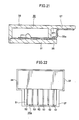
- Fig. 7 is a cross sectional view of a hybrid integrated circuit device according to a first embodiment of the present invention
- Fig. 8 is a plan view thereof.
- the hybrid integrated circuit device according to the present invention comprises a metal substrate 31, a casing member 32 and external leads 33.
- the metal substrate 31 comprises, for example, an aluminum substrate.
- An aluminum oxide film is formed on the surface of metal substrate 31 by anodic oxidation.
- An insulating film 34 is formed of resin such as epoxy resin or polyimide resin on the aluminum oxide film.
- copper foil is adhered on the insulating film 34.
- the copper foil is etched to be a desired pattern, so that conductive paths are formed.
- the conductive paths 35 extend along one major surface of the substrate 31 (in the direction of an arrow C in Fig. 7), and a plurality of conductive pads 36 to which external leads 33 are connected are formed in the tip portions thereof. As shown in Fig.
- a connector portion 37 is not provided in both ends 40 of the substrate 31, it should be considered that the conductive pads 36 are not formed around the corners of the substrate 31, so that the external leads 33 are arranged only on the connector portion 37 in the casing member 32.
- a plurality of circuit elements 38 such as a semiconductor integrated circuit, a transistor and a chip part are connected to the conductive paths 35.
- the casing member 32 comprises a sealing portion 39 surrounding the circuit elements 38 and the connector portion 37 supporting the external leads 33.
- the casing member 32 is injection-molded using insulating resin.
- the sealing portion 39 may have an arbitrary shape surrounding the circuit elements 38.
- the sealing portion 39 is formed in a box shape to fix the circumference excluding the pads 36 of the metal substrate 31 and hermetically seal the circuit elements 38.
- the connector portion 37 is formed in the shape projected from a bottom portion 391 of the box-shaped sealing portion 39 and extending beyond an end 311 of the metal substrate 31.
- the connector portion 37 is formed to be projected from the end 311 of the metal substrate 31 as described above, and the external leads 33 derived from the metal substrate 31 are arranged to contact a surface 371 (referred to as major surface hereinafter) opposed to the metal substrate 31.
- the external leads 33 may be fixed to the major surface 371 of the connector portion 37.
- the connector portion 37 is formed to be narrower than the sealing portion 39 for sealing the circuit elements 38.
- the width of the connector portion 37 can be arbitrarily changed according to the usage.
- the connector portion 37 is formed to be as thick as or thinner, by the thickness of the external leads 33 than a print board into which the connector portion is to be inserted.
- stepped portions 40 formed by the sealing portion 39 and the connector portion 37 serve as stoppers when the connector portion is inserted into the print board.
- an adhesive comprises an adhesive sheet.
- Fig. 9 is a cross sectional view of the hybrid integrated circuit device according to the present embodiment which is inserted into a print board 41.
- the connector portion 37 in the casing member 32 is inserted into an insertion hole 42 of the print board 41, and the external lead 33 is connected to an electrode 43 of the print board 41 by solder 44.
- the connector portion 37 can be automatically inserted into the print board using an automatic inserting apparatus.
- both the connector portion and the print board comprise insulating materials, an IC requiring large current and high breakdown voltage can be employed.
- Fig. 10 is a cross sectional view of a hybrid integrated circuit device according to the present embodiment
- Fig. 11 is a plan view thereof.
- the present embodiment is an improvement of a connector portion 37.
- notched portions 45 are provided in the intermediate portion of a major surface 371 of the connector portion 37 which an external lead 33 contacts, at the same pitch as the external leads 33.
- the external leads 33 are disposed in the notched portions 45.
- Fig. 12 illustrates a third embodiment.
- the present embodiment is an improvement of a connector portion 37.
- a hole 46 is provided near the tip portion on a major surface 371 of the connector portion 37 which an external lead 33 contacts, at the same pitch as the external leads 33.
- the tip portions of the external leads 33 are bent toward and inserted into the hole 46, so that the same effect of preventing offset as described above can be obtained.
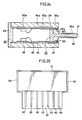
- FIG. 13 is a cross sectional view of a hybrid integrated circuit device according to the present embodiment
- Fig. 14 is a plan view thereof
- Fig. 15 is a cross sectional view of the hybrid integrated circuit device inserted into a print board according to the present embodiment.
- the present embodiment is an improvement of external leads 33 which contact a connector portion 37, wherein the external leads 33 which contact the connector portion 37 extend to a surface 372 opposite to a major surface 371 of the connector portion 37 along the outer surface of the connector portion 37.
- the connector portion 37 in a casing member 32 is inserted into an insertion hole 42 of a print board 41, and the external leads 33 are connected to an electrode 43 of the print board 41 by solder 44.
- the connection area of the external leads 33 is increased. For example, since current of 10 A to 40 A can be passed, the hybrid integrated circuit device can be employed with large current.
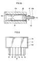
- FIG. 16 is a cross sectional view of a hybrid integrated circuit device according to the present embodiment
- Fig. 17 is a plan view thereof.
- the present embodiment is a further improvement of the connector portion 37 shown in Figs. 13 and 15.
- notched portions 47 are formed from the tip portions to the central portions on both surfaces, that is, surfaces 371 and 372 of the connector portion 37 which external leads contact, at the same pitch as the external leads 33.
- the external leads 33 are disposed in the notched portions 47. As a result, since the external leads 33 are limited in movement by the notched portions 47, offset of the leads 33 can be prevented.
- Fig. 18 illustrates a sixth embodiment.
- the present embodiment is an improvement of the connector portion 37 shown in Figs. 13 to 15.
- a hole 48 is provided near the intermediate portion of a surface 372 opposite to a major surface of a connector portion 37 in which the tip portions of the external leads 33 are located, at the same pitch as the external leads 33.
- the tip portions of the external leads 33 extending to the second major surface 372 of the connector portion 37 are bent toward and inserted into the hole 48.
- Fig. 19 illustrates a seventh embodiment.
- the present embodiment is an improvement of a casing member 32.
- the connector portion 37 is formed to be projected from the intermediate portion of a frame portion 321 in the casing member 32, so that spacing between a metal substrate 31 and a connector portion 37 can be decreased.
- the connector portion 37 is supported by a supporting member 49.
- the connector portion 37 is projected from the intermediate portion of the frame portion 321, the casing member 32 of an arbitrary shape may be formed by a metal mold.
- Fig. 20 illustrates an eighth embodiment.
- the present embodiment is an improvement of a connector portion 37.
- a slit 50 is formed between external leads 33 arranged on the connector portion 37. The slit 50 serves to prevent erroneous insertion into a print board.
- FIG. 21 is a cross sectional view of a hybrid integrated circuit device according to the present embodiment
- Fig. 22 is a plan view thereof
- Fig. 23 is a cross sectional view of the hybrid integrated circuit device according to the present embodiment which is inserted into a print board.
- the present embodiment is an improvement of external leads 33.
- an external lead comprises a flexible lead 33a.
- the flexible lead 33a comprises a heat resisting resin film 51, such as polyimide and polyamide and conductive paths 52 which are formed by adhering copper foil, for example, to the film 51 and etching it to be a pattern of a desired shape.
- the conductive paths 52 have an arbitrary pattern. According to the present embodiment, a plurality of substantially straight-line conductive paths 52 are formed. Since the flexible lead 33a is extremely thin, a connector portion 37 is formed to have the same thickness as that of a print board into which the connector portion 37 is to be inserted.
- the flexible lead 33a is connected to a major surface 371 of the connector portion 37 by a liquid adhesive to lie on the major surface 371 from the intermediate portion of the connector portion 37 to the tip portion of the connector portion 37.
- the flexible lead 33a is first connected to the pads 36 of the metal substrate 31, the flexible lead 33a may be connected to the conductive pads 36 after the flexible lead 33a is adhered in advance to the connector portion 37 and the substrate 31 and the casing member 32 are formed integrally with each other.
- the connector portion 37 in the casing member 32 is inserted into an insertion hole 42 of a print board 41. If and when an electrode 43 formed on the print board 41 is formed to extend to the insertion hole 42, the electrode 43 and the flexible lead 33a can be connected to each other by simply inserting the connector portion 37 into the hole 42.
- the flexible lead 33a is membranous and extremely thin, the flexible lead 33a catch nowhere when the hybrid integrated circuit device according to the present embodiment is inserted into the print board 41, so that the hybrid integrated circuit device is easily inserted.
- FIG. 24 illustrates a tenth embodiment.
- a hybrid integrated circuit device comprises two opposed metal substrates 61 and 61a. Metal oxide films are formed on the respective surfaces of metal substrates 61 and 61a, insulating films 64 and 64a are formed of resin on the metal oxide films, and conductive paths 65 and 65a are formed on the insulating films 64 and 64a. Conductive pads 66 and 66a to which external leads 63 and 63a are connected are formed in the tip portions of the conductive paths 65 and 65a.
- a plurality of circuit elements 68 and 68a such as a semiconductor integrated circuit, a transistor and a chip part are connected to the conductive paths 65 and 65a.
- a casing member 62 is disposed such that the two metal substrates 61 and 61a are spaced from each other.
- the circuit element 68 fixed to one metal substrate 61 is opposed to the circuit element 68a fixed to the other metal substrate 61a.
- the casing member 62 comprises a sealing portion 69 and a connector portion 67.
- the sealing portion 69 is formed in a frame shape to separate the metal substrate 61 and 61a and surround the circuit elements 68 and 68a.
- the connector portion 67 is formed to be projected from the intermediate portion of one surface 691 of the sealing portion 69 and to extend beyond the respective ends of the metal substrates 61 and 61a.
- One ends of the external leads 63 and 63a are soldered on the conductive pads 66 and 66a.
- the external leads 63 and 63a are molded to be bent to contact the connector portion 67, so that the tip portions thereof are located in the vicinity of the tip of the connector portion 67.
- the connector portion 67 is formed to be as wide as the sealing portion 69, or narrower than the sealing portion 69 as shown in Fig. 25. The width of the connector portion 67 can be changed according to the usage.
- the connector portion 67 is formed to be as thick as or thinner, by the thickness of the external leads 63 and 63a, than the print board into which the connector portion 67 is to be inserted.
- the metal substrates 61 and 61a and the casing member 62 are bonded by, for example, an adhesive sheet, as described in the first embodiment.
- the connector portion 67 in the casing member 62 is inserted into an insertion hole 42 of a print board 41, and the external leads 63 and 63a are soldered on electrodes 43 and 43a of the print board 41, respectively, as shown in Fig. 26.
- the shielding effect is large and the radiating effect is improved.
- circuit elements are mounted on two metal substrates, mounting can be achieved in high density.
- FIG. 27 is a cross sectional view of a hybrid integrated circuit device according to the present embodiment
- Fig. 28 is a plan view thereof
- Fig. 29 is a cross sectional view of the hybrid integrated circuit device according to the present embodiment which is inserted into a print board.
- external leads 63 and 63a are alternately folded on the side of another substrate. More specifically, conductive pads are not provided in positions opposed to each other, respectively, on metal substrates 61 and 61a, but alternately provided thereon. One ends of the external leads 63 and 63a are soldered on conductive pads 66 and 66a formed on the metal substrate 61 and 61a.
- the external leads 63 and 63a extend near the tip portion of a connector portion 67 along the connector portion 67, and bent to contact a surface on the opposite side of the connector portion in the end of the connector portion 67. At that time, since the conductive pads are alternately formed, one of the external leads 63 and 63a does not contact the other external lead on a surface on the opposite side even if the external leads 63 and 63a are bent on the opposite side of the connector portion. As shown in Fig.
- the connector portion 67 in a casing member 62 is inserted into an insertion hole 42 of a print board 41, and electrodes 43 and 43a of the print board 41 are connected by solder 44 on the external leads 63 and 63a, respectively.
- the external leads are bent in the connector portion as shown in Fig. 29, the connection areas of the external leads and the electrodes are large, so that an IC requiring large current and high breakdown voltage can be employed.
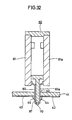
- FIG. 30 is a cross sectional view of a hybrid integrated circuit device according to the present embodiment
- Fig. 31 is a plan view thereof
- Fig. 32 is a cross sectional view of a hybrid integrated circuit device according to the present embodiment which is inserted into a print board.
- one ends of the external leads 63 and 63a are soldered on conductive pads 66 and 66a provided on metal substrates 61 and 61a.
- the external leads 63 and 63a extend to an end of a connector portion 67 along the connector portion 67.
- the tip portions of the external leads 63 and 63a may be bent in the end of the connector portion 67.
- the tip portions of the external leads 63 and 63a opposed to each other which are extending to the end of the connector portion 67 are connected to each other by solder 70.
- the external leads are dipped in solder. All of the external leads opposed to each other need not be connected to each other. It is necessary to connect to each other only the external leads required for electrical connection.
- the connector portion 67 in a casing member 62 is inserted into an insertion hole 42 of a print board 41, and an electrode 43 of the print board 41 is soldered on the external leads 63 and 63a.
- FIG. 33 is a cross sectional view of a hybrid integrated circuit device according to the present embodiment
- Fig. 34 is a plan view thereof
- Fig. 35 is a cross sectional view of the hybrid integrated circuit device according to the present embodiment which is inserted into a print board.
- all of the external leads opposed to each other are connected to each other.
- external leads opposed to each other are alternately connected to each other. More specifically, a long external lead and a short external lead are alternately connected to conductive pads of a metal substrate, and the long external lead is connected to a lead opposed to the long external lead by solder 70. As shown in Fig.
- the hybrid integrated circuit device and a print board are handled in the same manner, so that insertion can be simply made.
- the leads can be prevented from being bent, so that the hybrid integrated circuit device can be automatically inserted into the print board by an automatic inserting apparatus.
- a single metal substrate and a casing member are connected to each other, the effect of distortion or the like caused by thermal expansion can be completely neglected, as compared with the conventional hybrid integrated circuit device in which a plurality of substrates having different properties are formed integrally with each other.
- both surfaces are covered with metal, so that the shielding effect is increased and the radiating effect is improved.
- circuit elements are mounted on the two substrates, mounting can be achieved in high density.
Landscapes
- Engineering & Computer Science (AREA)
- Microelectronics & Electronic Packaging (AREA)
- Power Engineering (AREA)
- Physics & Mathematics (AREA)
- Condensed Matter Physics & Semiconductors (AREA)
- General Physics & Mathematics (AREA)
- Computer Hardware Design (AREA)
- Manufacturing & Machinery (AREA)
- Combinations Of Printed Boards (AREA)
- Coupling Device And Connection With Printed Circuit (AREA)
- Insulated Metal Substrates For Printed Circuits (AREA)
Applications Claiming Priority (14)
| Application Number | Priority Date | Filing Date | Title |
|---|---|---|---|
| JP61244371A JPS6398137A (ja) | 1986-10-15 | 1986-10-15 | 混成集積回路 |
| JP244371/86 | 1986-10-15 | ||
| JP247925/86 | 1986-10-17 | ||
| JP159715/86 | 1986-10-17 | ||
| JP159714/86 | 1986-10-17 | ||
| JP15971586U JPH0445253Y2 (fr) | 1986-10-17 | 1986-10-17 | |
| JP61247924A JPS63219149A (ja) | 1986-10-17 | 1986-10-17 | 混成集積回路 |
| JP247924/86 | 1986-10-17 | ||
| JP61247925A JPS63219187A (ja) | 1986-10-17 | 1986-10-17 | 混成集積回路 |
| JP15971486U JPH0715141Y2 (ja) | 1986-10-17 | 1986-10-17 | 混成集積回路 |
| JP160393/86 | 1986-10-20 | ||
| JP1986160393U JPH0639483Y2 (ja) | 1986-10-20 | 1986-10-20 | 混成集積回路 |
| JP176217/86 | 1986-11-17 | ||
| JP1986176217U JPS6380859U (fr) | 1986-11-17 | 1986-11-17 |
Publications (3)
| Publication Number | Publication Date |
|---|---|
| EP0264780A2 true EP0264780A2 (fr) | 1988-04-27 |
| EP0264780A3 EP0264780A3 (en) | 1988-12-14 |
| EP0264780B1 EP0264780B1 (fr) | 1992-03-11 |
Family
ID=27566213
Family Applications (1)
| Application Number | Title | Priority Date | Filing Date |
|---|---|---|---|
| EP87114938A Expired - Lifetime EP0264780B1 (fr) | 1986-10-15 | 1987-10-13 | Dispositif à circuit intégré hybride qui peut être inséré dans une douille |
Country Status (4)
| Country | Link |
|---|---|
| US (1) | US4884125A (fr) |
| EP (1) | EP0264780B1 (fr) |
| KR (1) | KR900007232B1 (fr) |
| DE (1) | DE3777324D1 (fr) |
Cited By (5)
| Publication number | Priority date | Publication date | Assignee | Title |
|---|---|---|---|---|
| EP0366338A2 (fr) * | 1988-10-26 | 1990-05-02 | Texas Instruments Incorporated | Substrat pour système de circuit électrique et système de circuit utilisant ce substrat |
| EP0469920A1 (fr) * | 1990-08-03 | 1992-02-05 | Mitsubishi Denki Kabushiki Kaisha | Méthode de fabrication d'un substrat isolant pour composant semi-conducteur, plaque métallique prégravée utilisée à cet effet |
| DE4238417A1 (fr) * | 1991-11-14 | 1993-05-19 | Mitsubishi Electric Corp | |
| EP0621746A2 (fr) * | 1993-04-20 | 1994-10-26 | Lambda Electronics, Inc. | Plaque à circuit imprimé composite et son procédé de fabrication |
| WO2000074445A1 (fr) * | 1999-05-31 | 2000-12-07 | Tyco Electronics Logistics Ag | Module de puissance intelligent de structure sandwich |
Families Citing this family (5)
| Publication number | Priority date | Publication date | Assignee | Title |
|---|---|---|---|---|
| JPH05175520A (ja) * | 1991-12-20 | 1993-07-13 | Fujitsu Ltd | 光電気回路混載モジュール |
| JP3161142B2 (ja) * | 1993-03-26 | 2001-04-25 | ソニー株式会社 | 半導体装置 |
| JP2001068742A (ja) * | 1999-08-25 | 2001-03-16 | Sanyo Electric Co Ltd | 混成集積回路装置 |
| KR100630960B1 (ko) * | 2004-10-05 | 2006-10-02 | 삼성전자주식회사 | Pcb조립체 |
| JP2006140192A (ja) * | 2004-11-10 | 2006-06-01 | Matsushita Electric Ind Co Ltd | 電子回路装置 |
Citations (4)
| Publication number | Priority date | Publication date | Assignee | Title |
|---|---|---|---|---|
| US3605999A (en) * | 1969-07-23 | 1971-09-20 | Aerojet General Co | Insulative coated metal substrates and apparatus for holding substrates |
| JPS61166148A (ja) * | 1985-01-18 | 1986-07-26 | Sanyo Electric Co Ltd | 多層混成集積回路装置 |
| JPS61166149A (ja) * | 1985-01-18 | 1986-07-26 | Sanyo Electric Co Ltd | 多層混成集積回路装置 |
| JPS61242053A (ja) * | 1985-04-19 | 1986-10-28 | Sanyo Electric Co Ltd | 半導体装置 |
Family Cites Families (4)
| Publication number | Priority date | Publication date | Assignee | Title |
|---|---|---|---|---|
| JPS57188858A (en) * | 1981-05-18 | 1982-11-19 | Matsushita Electronics Corp | Plastic molded type semiconductor device |
| US4524238A (en) * | 1982-12-29 | 1985-06-18 | Olin Corporation | Semiconductor packages |
| US4805009A (en) * | 1985-03-11 | 1989-02-14 | Olin Corporation | Hermetically sealed semiconductor package |
| US4715115A (en) * | 1986-04-03 | 1987-12-29 | Hewlett-Packard Company | Package for water-scale semiconductor devices |
-
1987
- 1987-10-13 EP EP87114938A patent/EP0264780B1/fr not_active Expired - Lifetime
- 1987-10-13 DE DE8787114938T patent/DE3777324D1/de not_active Expired - Lifetime
- 1987-10-13 US US07/107,990 patent/US4884125A/en not_active Expired - Lifetime
- 1987-10-14 KR KR1019870011409A patent/KR900007232B1/ko not_active IP Right Cessation
Patent Citations (4)
| Publication number | Priority date | Publication date | Assignee | Title |
|---|---|---|---|---|
| US3605999A (en) * | 1969-07-23 | 1971-09-20 | Aerojet General Co | Insulative coated metal substrates and apparatus for holding substrates |
| JPS61166148A (ja) * | 1985-01-18 | 1986-07-26 | Sanyo Electric Co Ltd | 多層混成集積回路装置 |
| JPS61166149A (ja) * | 1985-01-18 | 1986-07-26 | Sanyo Electric Co Ltd | 多層混成集積回路装置 |
| JPS61242053A (ja) * | 1985-04-19 | 1986-10-28 | Sanyo Electric Co Ltd | 半導体装置 |
Non-Patent Citations (3)
| Title |
|---|
| PATENT ABSTRACTS OF JAPAN, vol. 10, no. 370 (E-463)[2427, 10th December 1986; & JP-A-61 166 148 (SANYO ELECTRIC CO., LTD) 26-07-1986 * |
| PATENT ABSTRACTS OF JAPAN, vol. 10, no. 370 (E-463)[2427], 10th December 1986; & JP-A-61 166 149 (SANYO ELECTRIC CO., LTD) 26-07-1986 * |
| PATENT ABSTRACTS OF JAPAN, vol. 11, no. 88 (E-490)[2535], 18th March 1987; &-JP-A-61 242 053 (SANYO ELECTRIC CO., LTD) 28-10-1986 * |
Cited By (8)
| Publication number | Priority date | Publication date | Assignee | Title |
|---|---|---|---|---|
| EP0366338A2 (fr) * | 1988-10-26 | 1990-05-02 | Texas Instruments Incorporated | Substrat pour système de circuit électrique et système de circuit utilisant ce substrat |
| EP0366338A3 (fr) * | 1988-10-26 | 1990-11-22 | Texas Instruments Incorporated | Substrat pour système de circuit électrique et système de circuit utilisant ce substrat |
| EP0469920A1 (fr) * | 1990-08-03 | 1992-02-05 | Mitsubishi Denki Kabushiki Kaisha | Méthode de fabrication d'un substrat isolant pour composant semi-conducteur, plaque métallique prégravée utilisée à cet effet |
| US5271993A (en) * | 1990-08-03 | 1993-12-21 | Mitsubishi Denki Kabushiki Kaisha | Method of manufacturing insulation substrate for semiconductor device and metal pattern plate used therefor |
| DE4238417A1 (fr) * | 1991-11-14 | 1993-05-19 | Mitsubishi Electric Corp | |
| EP0621746A2 (fr) * | 1993-04-20 | 1994-10-26 | Lambda Electronics, Inc. | Plaque à circuit imprimé composite et son procédé de fabrication |
| EP0621746A3 (fr) * | 1993-04-20 | 1995-04-12 | Lambda Electronics Inc | Plaque à circuit imprimé composite et son procédé de fabrication. |
| WO2000074445A1 (fr) * | 1999-05-31 | 2000-12-07 | Tyco Electronics Logistics Ag | Module de puissance intelligent de structure sandwich |
Also Published As
| Publication number | Publication date |
|---|---|
| KR900007232B1 (ko) | 1990-10-05 |
| EP0264780B1 (fr) | 1992-03-11 |
| US4884125A (en) | 1989-11-28 |
| DE3777324D1 (de) | 1992-04-16 |
| KR880005685A (ko) | 1988-06-30 |
| EP0264780A3 (en) | 1988-12-14 |
Similar Documents
| Publication | Publication Date | Title |
|---|---|---|
| EP0001892B1 (fr) | Grille de conducteurs et boîtier pour établir des connexions électriques à composants électroniques | |
| US9692156B2 (en) | Electronic device | |
| US5352851A (en) | Edge-mounted, surface-mount integrated circuit device | |
| US4949225A (en) | Circuit board for mounting electronic components | |
| US4885662A (en) | Circuit module connection system | |
| EP0264780B1 (fr) | Dispositif à circuit intégré hybride qui peut être inséré dans une douille | |
| US5107329A (en) | Pin-grid array semiconductor device | |
| KR100226335B1 (ko) | 플라스틱 성형회로 패키지 | |
| US5444299A (en) | Electronic package with lead wire connections | |
| JP3549653B2 (ja) | チップ型電子部品 | |
| JPH0445253Y2 (fr) | ||
| JPH0639483Y2 (ja) | 混成集積回路 | |
| JP3894336B2 (ja) | 電子部品 | |
| JPH0715141Y2 (ja) | 混成集積回路 | |
| GB2204740A (en) | Housings for electrical components | |
| JPS63219149A (ja) | 混成集積回路 | |
| JP3137212B2 (ja) | フレキシブル配線板 | |
| JPH0531839B2 (fr) | ||
| JP3615236B2 (ja) | 混成集積回路装置 | |
| JPH0519974Y2 (fr) | ||
| JPH0469820B2 (fr) | ||
| JP2771575B2 (ja) | 混成集積回路 | |
| JPS62179794A (ja) | 電気回路配線板 | |
| JPH08204305A (ja) | 混成集積回路装置 | |
| JPH03159186A (ja) | 混成集積回路装置 |
Legal Events
| Date | Code | Title | Description |
|---|---|---|---|
| PUAI | Public reference made under article 153(3) epc to a published international application that has entered the european phase |
Free format text: ORIGINAL CODE: 0009012 |
|
| AK | Designated contracting states |
Kind code of ref document: A2 Designated state(s): DE GB NL |
|
| PUAL | Search report despatched |
Free format text: ORIGINAL CODE: 0009013 |
|
| AK | Designated contracting states |
Kind code of ref document: A3 Designated state(s): DE GB NL |
|
| 17P | Request for examination filed |
Effective date: 19890104 |
|
| 17Q | First examination report despatched |
Effective date: 19910412 |
|
| GRAA | (expected) grant |
Free format text: ORIGINAL CODE: 0009210 |
|
| AK | Designated contracting states |
Kind code of ref document: B1 Designated state(s): DE GB NL |
|
| REF | Corresponds to: |
Ref document number: 3777324 Country of ref document: DE Date of ref document: 19920416 |
|
| PLBE | No opposition filed within time limit |
Free format text: ORIGINAL CODE: 0009261 |
|
| STAA | Information on the status of an ep patent application or granted ep patent |
Free format text: STATUS: NO OPPOSITION FILED WITHIN TIME LIMIT |
|
| 26N | No opposition filed | ||
| REG | Reference to a national code |
Ref country code: GB Ref legal event code: IF02 |
|
| PGFP | Annual fee paid to national office [announced via postgrant information from national office to epo] |
Ref country code: NL Payment date: 20051016 Year of fee payment: 19 |
|
| PGFP | Annual fee paid to national office [announced via postgrant information from national office to epo] |
Ref country code: DE Payment date: 20061005 Year of fee payment: 20 |
|
| PGFP | Annual fee paid to national office [announced via postgrant information from national office to epo] |
Ref country code: GB Payment date: 20061011 Year of fee payment: 20 |
|
| PG25 | Lapsed in a contracting state [announced via postgrant information from national office to epo] |
Ref country code: NL Free format text: LAPSE BECAUSE OF NON-PAYMENT OF DUE FEES Effective date: 20070501 |
|
| NLV4 | Nl: lapsed or anulled due to non-payment of the annual fee |
Effective date: 20070501 |
|
| REG | Reference to a national code |
Ref country code: GB Ref legal event code: PE20 |
|
| PG25 | Lapsed in a contracting state [announced via postgrant information from national office to epo] |
Ref country code: GB Free format text: LAPSE BECAUSE OF EXPIRATION OF PROTECTION Effective date: 20071012 |