EP0258060B1 - Vorrichtung für die Steuerung der Lichtmenge - Google Patents
Vorrichtung für die Steuerung der Lichtmenge Download PDFInfo
- Publication number
- EP0258060B1 EP0258060B1 EP87307608A EP87307608A EP0258060B1 EP 0258060 B1 EP0258060 B1 EP 0258060B1 EP 87307608 A EP87307608 A EP 87307608A EP 87307608 A EP87307608 A EP 87307608A EP 0258060 B1 EP0258060 B1 EP 0258060B1
- Authority
- EP
- European Patent Office
- Prior art keywords
- current
- light quantity
- semiconductor laser
- voltage
- outputs
- Prior art date
- Legal status (The legal status is an assumption and is not a legal conclusion. Google has not performed a legal analysis and makes no representation as to the accuracy of the status listed.)
- Expired - Lifetime
Links
Images


Classifications
-
- H—ELECTRICITY
- H01—ELECTRIC ELEMENTS
- H01S—DEVICES USING THE PROCESS OF LIGHT AMPLIFICATION BY STIMULATED EMISSION OF RADIATION [LASER] TO AMPLIFY OR GENERATE LIGHT; DEVICES USING STIMULATED EMISSION OF ELECTROMAGNETIC RADIATION IN WAVE RANGES OTHER THAN OPTICAL
- H01S5/00—Semiconductor lasers
- H01S5/06—Arrangements for controlling the laser output parameters, e.g. by operating on the active medium
- H01S5/068—Stabilisation of laser output parameters
- H01S5/0683—Stabilisation of laser output parameters by monitoring the optical output parameters
-
- G—PHYSICS
- G06—COMPUTING OR CALCULATING; COUNTING
- G06K—GRAPHICAL DATA READING; PRESENTATION OF DATA; RECORD CARRIERS; HANDLING RECORD CARRIERS
- G06K15/00—Arrangements for producing a permanent visual presentation of the output data, e.g. computer output printers
- G06K15/02—Arrangements for producing a permanent visual presentation of the output data, e.g. computer output printers using printers
- G06K15/12—Arrangements for producing a permanent visual presentation of the output data, e.g. computer output printers using printers by photographic printing, e.g. by laser printers
- G06K15/1204—Arrangements for producing a permanent visual presentation of the output data, e.g. computer output printers using printers by photographic printing, e.g. by laser printers involving the fast moving of an optical beam in the main scanning direction
- G06K15/1209—Intensity control of the optical beam
- G06K15/1214—Intensity control of the optical beam by feedback
-
- H—ELECTRICITY
- H01—ELECTRIC ELEMENTS
- H01S—DEVICES USING THE PROCESS OF LIGHT AMPLIFICATION BY STIMULATED EMISSION OF RADIATION [LASER] TO AMPLIFY OR GENERATE LIGHT; DEVICES USING STIMULATED EMISSION OF ELECTROMAGNETIC RADIATION IN WAVE RANGES OTHER THAN OPTICAL
- H01S5/00—Semiconductor lasers
- H01S5/04—Processes or apparatus for excitation, e.g. pumping, e.g. by electron beams
- H01S5/042—Electrical excitation ; Circuits therefor
-
- H—ELECTRICITY
- H01—ELECTRIC ELEMENTS
- H01S—DEVICES USING THE PROCESS OF LIGHT AMPLIFICATION BY STIMULATED EMISSION OF RADIATION [LASER] TO AMPLIFY OR GENERATE LIGHT; DEVICES USING STIMULATED EMISSION OF ELECTROMAGNETIC RADIATION IN WAVE RANGES OTHER THAN OPTICAL
- H01S5/00—Semiconductor lasers
- H01S5/06—Arrangements for controlling the laser output parameters, e.g. by operating on the active medium
- H01S5/0617—Arrangements for controlling the laser output parameters, e.g. by operating on the active medium using memorised or pre-programmed laser characteristics
-
- H—ELECTRICITY
- H01—ELECTRIC ELEMENTS
- H01S—DEVICES USING THE PROCESS OF LIGHT AMPLIFICATION BY STIMULATED EMISSION OF RADIATION [LASER] TO AMPLIFY OR GENERATE LIGHT; DEVICES USING STIMULATED EMISSION OF ELECTROMAGNETIC RADIATION IN WAVE RANGES OTHER THAN OPTICAL
- H01S5/00—Semiconductor lasers
- H01S5/06—Arrangements for controlling the laser output parameters, e.g. by operating on the active medium
- H01S5/068—Stabilisation of laser output parameters
- H01S5/06812—Stabilisation of laser output parameters by monitoring or fixing the threshold current or other specific points of the L-I or V-I characteristics
-
- H—ELECTRICITY
- H01—ELECTRIC ELEMENTS
- H01S—DEVICES USING THE PROCESS OF LIGHT AMPLIFICATION BY STIMULATED EMISSION OF RADIATION [LASER] TO AMPLIFY OR GENERATE LIGHT; DEVICES USING STIMULATED EMISSION OF ELECTROMAGNETIC RADIATION IN WAVE RANGES OTHER THAN OPTICAL
- H01S5/00—Semiconductor lasers
- H01S5/06—Arrangements for controlling the laser output parameters, e.g. by operating on the active medium
- H01S5/068—Stabilisation of laser output parameters
- H01S5/0683—Stabilisation of laser output parameters by monitoring the optical output parameters
- H01S5/06832—Stabilising during amplitude modulation
Definitions
- a laser beam printer in which a photosensitive member is scanned with a laser beam modulated according to input information to form an electrostatic latent image, and said latent image is rendered visible with magnetic developing powder, called toner, allowing it to be transferred onto a recording material, such as paper.
- Figure 12 illustrates an example of such a conventional laser beam printer in which a photosensitive drum 1, having a semiconductor surface layer of selenium or cadmium sulphide, is rotatably supported in a housing and rotated at a constant speed in a direction A.
- a semiconductor laser 2 and a control circuit 2A are also provided for intensity and on-off control of the laser beam from the laser 2.
- the laser beam L emitted by the semiconductor laser 2 is expanded to a predetermined diameter by a beam expander 3, and then enters a polygon mirror 4 having plural mirror faces and rotated at a fixed speed by a scanner motor 5, whereby said laser beam is deflected by said polygon mirror to perform a scanning motion in the substantially horizontal direction. Then the beam is focused, by an imaging lens 6 of f- ⁇ characteristic, as a light spot on the photosensitive drum 1 previously charged to a predetermined polarity by a charger 13.
- the laser beam reflected by a mirror 8 is detected by a detector 7, of which detection signal determines the timing of modulation of the semiconductor laser 2 for obtaining desired light information on the photosensitive drum 1.
- a detector 7 On said drum 1, an electrostatic latent image is formed by the scanning laser beam, according to the above-mentioned input information.
- Said latent image is rendered visible by toner deposition in a developer unit 9, and the visible image thus obtained is transferred onto a recording material, usually paper, fed from a cassette 10 or 11.
- the recording material then passes a fixing unit 12 for fixing said image to the material, and is discharged to an unrepresented tray.
- the semiconductor laser usually employed in such laser beam printer has an I - l characteristic, or the relation of the laser driving current and the emitted light quantity, as shown in Fig. 13.
- the semiconductor laser does not emit a beam until the current reaches a threshold value (I th ), but emits the laser beam when said threshold value is exceeded.
- the light quantity l shows a certain inclination ⁇ as a function of the laser driving current, and said ⁇ is called slope efficiency.
- control circuit 2A controls the light quantity of the semiconductor laser 2 and determines the laser current I T so as to obtain a predetermined light quantity l T , and this light quantity is maintained constant by the supply of constant laser current I T .
- the I - l characteristic of the semiconductor laser which has an initial form A as shown in Fig. 14, during a constant current drive with a laser current I T for obtaining a predetermined light quantity l TA , may vary to a form B or C for example due to an increase in the chip temperature caused by the current in the semiconductor laser.
- the above-explained latent image may not be formed if the I - l characteristic changes to B shown in Fig. 14 due to the increase in temperature so that the light quantity of the laser decreases to l TB despite that the laser current is maintained at I T .
- the laser chip may be destructed if the light quantity increases to l TC as indicated by C.
- the present applicant already proposed light quantity controlling devices in the US Patents 4,201,994 and 4,443,695 but sufficient effect could not be achieved by the processes disclosed in these patent applications.
- the present invention is concerned with reducing the above-mentioned drawbacks.
- a light quantity control device according to the preamble of claim 1 is known from EP-A-0 061 034.
- a light quantity control device as set out in claim 1.
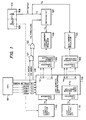
- Fig. 1 is a block diagram of the principal part of an embodiment of the present invention.
- Fig. 1 there are shown a central processing unit (CPU) 101 for controlling the entire information recording apparatus; a laser light quantity comparator/controller l02 composed of a one-chip microcomputer incorporating an analog-to-digital (A/D) converter for effecting light quantity control as shown in Fig. 2 according to a control sequence as shown in Fig.
- CPU central processing unit
- l02 composed of a one-chip microcomputer incorporating an analog-to-digital (A/D) converter for effecting light quantity control as shown in Fig. 2 according to a control sequence as shown in Fig.
- A/D analog-to-digital
- a bias current control circuit 103 having a digital-to-analog (D/A) converter connected to outputs Bl - Bn of the light quantity comparator/controller 102; a bias current regulator 104 receiving the bias current I B and controlled by the circuit 103; a light emission current control circuit 105 having a D/A converter connected to other outputs Dl - Dn of the light quantity comparator/controller 102; and a light emission current regulator 106 controlled by said circuit 105 and receiving the light emission current I D through a light emission current switching circuit 107.
- D/A digital-to-analog
- a semiconductor laser 108 there are further provided a semiconductor laser 108; a photodiode 109 for receiving the light beam from said laser 108; a light quantity monitor circuit 110 for receiving a detection signal from the photodiode 109 and supplying the light quantity comparator/controller with a voltage V M corresponding to the detected light quantity; a light quantity setting circuit 111 for setting the light quantity of the laser; an AND gate 121; and an OR gate 122.
- the light quantity comparator/controller 102 clears, in a step 202, all the input signals Dl - Dn, Bl - Bn for the D/A converter of the bias current control circuit 103 and the light emission current control circuit 105 thereby sufficiently reducing the laser current I l (light emission current I D + bias current I B ) in the semiconductor laser 108 (for example setting a laser current I l in the laser unit) through the light emission current regulator 106 and the bias current regulator 104.
- a next step 203 shifts the video (image) signal LON 116 to a true level, to open the gate of the switching circuit 107, thereby supplying the semiconductor laser 108 with a light emission current.
- the light emission current control circuit 105 and the bias current control circuit 103 are provided with digital-to-analog converting circuits, such as the D/A converters, and count up or down the digital output signals Dl - Dn and Bl - Bn from the light quantity comparator/controller 102, thereby varying the laser current I in the laser by an analog value corresponding to said up-count or down-count, through the light emission current regualtor 106 or the bias current regulator 104.
- digital-to-analog converting circuits such as the D/A converters
- the bias count X B counted by the bias current control circuit 103 is represented by an n-bit binary number having the output Bl of the light quantity comparator/controller 102 as the least significant bit (LSB) and the output Bn as the most significant bit (MSB), and is explained as being counted up or down.
- Fig. 4A shows a state of counting up the bias count X B wherein "0" indicates a low or false level, while "1" indicates a high or true level.
- the bias current I B increases proportionally with the increase of the bias count X B .
- the light emitted by the semiconductor laser 108 is photoelectrically converted by the photodiode 109 in the laser unit 112 and is processed by the light quantity monitor circuit 110 to obtain a monitor voltage V M , as shown in Fig. 5, for feedback to the light quantity comparator/controller 102.
- a bias current control is conducted in a sequence starting from a step 203.
- the bias current count X B is counted up stepwise while the light emission count X D is maintained at "0" (step 204), whereby a laser current corresponding to thus increasing count X B is supplied to the semiconductor laser 108 through the bias current regulator 104.
- the detected value of the light emitted by said laser current is fed back, through the light quantity monitor circuit 110, to the light quantity comparator/controller 102.
- the semiconductor laser 108 emits a beam when the laser current exceeds a threshold current I th . Then the bias current count X B is increased to increase the laser current in the semiconductor laser 108. The up-counting of the bias current count X B is terminated when the monitor voltage V M reaches a bias current specifying voltage V B0 (step 205).
- the bias current count in this state is defined as the bias current specifying count X B0 .
- the laser 108 emits a laser beam with an intensity which may be enough for forming a latent image on the photosensitive drum 1. Consequently the bias current actually employed is defined by a count X BT obtained by multiplying a constant value (for example 80%) on said specifying count X B0 (step 206).
- the current in the laser 108 corresponding to the bias current setting count X BT , is definded as the set bias current I BT .
- the bias voltage V M is confirmed while the set bias current I BT is supplied to the semiconductor laser 108, and the absolute value of the difference of the monitor voltage V M and the bias current specifying voltage V B0 exceeds the voltage V B0 multiplied by a constant a (step 207), the sequence returns to the step 202, in order to reset the bias current count X B to "0", thereby terminating the laser current, and to repeat the bias current control from the beginning.
- the sequence proceeds from the steps 207 to 208.
- the light emission current is controlled while said set bias current I BT is supplied to the semiconductor laser 108.
- the video signal is shifted to the true level, in order to open the gate in the switch circuit 107, thereby enabling the supply of the light emission current I D to the semiconductor laser 108.
- the control of the light emission current is conducted by maintaining the bias current count X B at the bias current setting count X BT thereby supplying the semiconductor laser 108 with the set bias current I BT .
- the light emission count X D is increased stepwise from "0" (step 208).
- the intensity of the laser beam caused by the laser current Il is photoelectrically converted by the photodiode 109 incorporated in the semiconductor laser unit 112 and is fed back, by the light quantity monitor circuit 110, to the light quantity comparator/controller 102.
- the light emission current I D increases, thereby increasing the intensity of the laser beam.
- the increase in the light quantity is detected by the increase in the monitor voltage V M .
- the light emission count X D is counted up to increase the current in the laser 108, and the up-counting of the light emission count X D is terminated when the monitor voltage V M reaches the light quantity specifying voltage V D (step 209).
- the light emission current count in this state is defined as the light emission current setting count X DT .
- the monitor voltage V M is confirmed while said set light emission current is supplied to the semiconductor laser 108. If the monitor voltage V M is not within a predetermined range (for example ⁇ 5%) with respect to the light quantity specifying voltage V D (step 210), the light emission current count X D is cleared (step 211) to terminate the light emission current I D , and the sequence returns to the step 208 to repeat the light emission current control.
- the monitor voltage V M is within said range with respect to the light quantity specifying voltage V D and the APCST signal from the central processing unit 101 is in the false level, the light emission current setting count X DT and the bias current setting count X BT are retained but the gate of the switching circuit 107 is closed to limit the current in the laser 108 only to the bias setting current I BT . Also in case said APCST signal is in the true level, the gate of the switching circuit 107 is maintained open, and is closed when the APCST signal is shifted to the false level.
- the light quantity specifying voltage V D mentioned above is determined in the following manner.
- the light quantity setting voltage V 0 is determined by the light quantity setting circuit 111.
- Said voltage V 0 may be obtained by a voltage division with resistors as shown in Fig. 6.
- Said voltage V 0 supplied to the light quantity comparator/controller 102 is corrected by the sensitivity of the photosensitive drum 1, supplied by signals 114 (CSEN1, CSEN2) from the central processing unit l.
- the correcting value for V 0 is represented for example as +10% or -10% with respect to the central value V 0 , and thus corrected value is defined as the light quantity specifying voltage V D .
- the bias count X B and the light emission count X D are respectively increased by one step until the monitor voltage V M reaches the bias current specifying voltage V B0 or the light quantity specifying voltage V D (steps 204, 208 in Fig. 3).
- the present embodiment employs a high-speed and high-precision light quantity control as shown in Figs. 15 and 16.
- This control operation will be explained in the following according to the flow chart shown in Fig. 16. In this operation the sequences of the regions A and B in Fig. 3 are replaced by those in Fig. 16. Thus, after the steps 203 and 207 shown in Fig. 3, there is executed a step 301 shown in Fig.
- a next step 302 increases the bias count X B (or the light emission count X D ) by 3 counts at a time.
- a step 303 compares the voltage V M with another proportion V B0 ⁇ (or V D ⁇ ) of the voltage V B0 (or V D ) and, if the monitor voltage V M is smaller, a step 304 increases the count X B (or X D ) by 2 counts at a time.
- a step 305 compares the monitor voltage V M with the bias specifying voltage V B0 (or the light emission specifying voltage V D ), and, if the monitor voltage V M is smaller, the count X B (or X D ) is increased by one count at a time until the monitor voltage V M reaches V B0 (or V D ).
- V M reaches V B0 (or V D )
- the sequence proceeds to the step 206 or 210 shown in Fig. 3.
- the above-explained sequence enables automatic light quantity control of high precision within a short time as shown in Fig. 15.
- the parenthesized portions correspond to the region B in Fig. 3.
- the laser current Il is increased by the up-counting of the bias count X B , and, if the monitor voltage V M does not reach the bias current specifying voltage V B0 even at a time T B where the bias count X B is at the maximum value, the bias current is determined as the current I BMAX at said maximum bias count, or a predetermined proportion of said current I BMAX .
- the control of the light emission current is conducted under the presence of a predetermined bias current.
- the laser current is increased by up-counting of the light emission count X D , and, if the monitor voltage V M does not reach the light quantity specifying voltage V D at a time T D when the light emission count X D reaches maximum, the control of the light emission current is terminated in the presence of a light emission current I DMAX at said maximum light emission count.
- Fig. 8 shows the circuit structure other than the laser controller 50l detailedly shown in Fig. 1.
- a scanner motor control circuit 503 controls the scanner motor control circuit 503 and the rotation control circuit 504, controlled for example through known integrated circuits for PLL control, and the detecting circuit 505 composed of microswitches or photointerruptors.
- the CPU 101 also receives a print control signal (PRINT) 506 or a video signal 507 from an operation panel or a reader unit, and a test signal (MLON) 508 from an external control unit, and controls the laser control circuit 50l shown in Fig. 1 in response to these signals.
- PRINT print control signal
- MLON test signal
- a step 602 shifts a drum drive signal (DRMD) 513 and a scanner motor drive signal (SCNON) 509 to the true level. Then a step 603 confirms a SCNRDY signal 510 indicating that the scanner motor is ready, and a step 604 shifts the auto light quantity control start signal (APCST) 113 to the true level.
- DRMD drum drive signal
- SCNON scanner motor drive signal
- a step 605 the light quantity comparator/controller 102 of the laser controller 501 effects the automatic light quantity control of the semiconductor laser 108. Then, when the drum drive signal (DRMD) 513 or the scanner motor rotation ready signal (SCNRY) 510 is shifted to the false state in a step 606, a next step 607 clears the bias count X B and the light emission count X D through the light quantity comparator/controller 102, thereby sufficiently reducing the current in the semiconductor laser 108.
- DRMD drum drive signal
- SCNRY scanner motor rotation ready signal
- the operation of the step 607 may be executed when the drum drive signal (DRMD) 513 is shifted to the false level, or within a certain period before or after such shifting to the flase level.
- DRMD drum drive signal
- the APCST signal 113 assumes the true level, in case of a continuous printing operation, between successive printing operations, i.e. in the non-image area between successive recording sheets as shown in Fig. 11, and the automatic light quantity control is completed within said non-image area. Also if the APCST signal 113 is not generated over a predetermined period T APC , the automatic light quantity control is conducted after said period T APC .
- a TOPER signal 601 shown in Fig. 11 indicates the above mentioned non-image area.
Landscapes
- Physics & Mathematics (AREA)
- Optics & Photonics (AREA)
- Engineering & Computer Science (AREA)
- General Physics & Mathematics (AREA)
- General Engineering & Computer Science (AREA)
- Theoretical Computer Science (AREA)
- Condensed Matter Physics & Semiconductors (AREA)
- Electromagnetism (AREA)
- Laser Beam Printer (AREA)
- Semiconductor Lasers (AREA)
- Facsimile Scanning Arrangements (AREA)
- Mechanical Optical Scanning Systems (AREA)
Claims (6)
- Lichtmengensteuerungsvorrichtung miteinem Halbleiterlaser (108),einer Überwachungseinrichtung (109, 110) zum Erzeugen einer Überwachungsspannung (VM) entsprechend der erfaßten Lichtmenge eines durch den Halbleiterlaser (108) erzeugten Strahls undeiner Steuerungseinrichtung zur Steuerung der Lichtmenge des durch den Halbleiterlaser (108) erzeugten Strahls im Ansprechen auf die Überwachungsspannung (VM) und eine Einstellspannung (V0) aus einer Lichtmengeneinstellschaltung, wobei die Steuerungseinrichtungdadurch gekennzeichnet, daßeine Vergleichs-/Steuerungseinrichtung (102) mit einer Analog-Digital-Umwandlungseinrichtung (A/D) zur Umwandlung der Überwachungsspannung (VM) undeine erste Stromsteuerungsschaltung (103) mit einem an ersten Ausgängen (B1-Bn) der Vergleichs-/Steuerungseinrichtung (102) angeschlossenen Digital-Analog-Umwandler zur Steuerung eines zu dem Halbleiterlaser (108) zugeführten ersten Stroms (IB) aufweist,die Steuerungseinrichtung eine zweite Stromsteuerungsschaltung (105) mit einer an zweiten Ausgängen (D1-Dn) der Vergleichs-/Steuerungseinrichtung (102) angeschlossenen Digital-Analog-Umwandlungseinrichtung aufweist zur Steuerung eines dem Halbleiterlaser (108) zusätzlich zu dem ersten Strom (IB) zugeführten zweiten Stroms (ID),die Vergleichs-/Steuerungseinrichtung (102) nacheinander betrieben wird, um den Digitalwert der ersten Ausgänge (B1-Bn) zu aktualisieren, bis die Überwachungsspannung (VM) eine einen Schwellenwert des Halbleiterlasers überschreitende vorbestimmte Spannung (VB0) erreicht, und danach nacheinander den Digitalwert an den zweiten Ausgängen (D1-Dn) aktualisiert, bis die Überwachungsspannung (VM) eine von der Einstellspannung (V0) hergeleitete Lichtmengen-Bestimmungsspannung (VD) erreicht, undder Betrag, auf den der erste Strom (IB) geändert wird, wenn die ersten Ausgangssignale (B1-Bn) aktualisiert werden, größer ist als der Betrag auf den der zweite Strom (ID) geändert wird, wenn die zweiten Ausgangssignale (D1-Dn) aktualisiert werden.
- Vorrichtung nach Anspruch 1,
dadurch gekennzeichnet, daß
die Vergleichs-/Steuerungseinrichtung (102) deren erste und zweite Ausgangssignale (B1-Bn;D1-Dn) in Einheitsschrittgröße erhöht. - Vorrichtung nach Anspruch 1,
dadurch gekennzeichnet, daß
die Vergleichs-/Steuerungseinrichtung (102) deren erste und zweite Ausgangssignale (B1-Bn;D1-Dn) in von dem Wert der Überwachungsspannung (VM) abhängigen unterschiedlichen Schrittgrößen erhöht. - Vorrichtung nach Anspruch 1, 2 oder 3,
dadurch gekennzeichnet, daß
der Halbleiterlaser und das Erfassungselement (109) der Überwachungseinrichtung in derselben Einheit (112) ausgebildet sind. - Verwendung einer Vorrichtung nach einem der vorangehenden Ansprüche, zur
Strahlintensitätssteuerung eines bei einem Druckvorgang verwendeten Halbleiterlasers. - Verwendung einer Vorrichtung nach einem der Ansprüche 1 bis 4, zur
Strahlintensitätssteuerung eines bei einem ununterbrochenen Druckvorgang verwendeten Halbleiterlasers, wobei die Strahlintensitätssteuerung durch die Stromsteuerungsschaltungen (103, 105) zwischen aufeinanderfolgenden Druckvorgängen ausgelöst wird.
Applications Claiming Priority (8)
| Application Number | Priority Date | Filing Date | Title |
|---|---|---|---|
| JP61198988A JPH07115486B2 (ja) | 1986-08-27 | 1986-08-27 | 記録装置 |
| JP61198990A JPH0754957B2 (ja) | 1986-08-27 | 1986-08-27 | 記録装置の光量制御装置 |
| JP61198989A JPH07100374B2 (ja) | 1986-08-27 | 1986-08-27 | 記録装置 |
| JP61198991A JPH07100377B2 (ja) | 1986-08-27 | 1986-08-27 | レ−ザ記録装置 |
| JP198989/86 | 1986-08-27 | ||
| JP198990/86 | 1986-08-27 | ||
| JP198988/86 | 1986-08-27 | ||
| JP198991/86 | 1986-08-27 |
Publications (3)
| Publication Number | Publication Date |
|---|---|
| EP0258060A2 EP0258060A2 (de) | 1988-03-02 |
| EP0258060A3 EP0258060A3 (de) | 1989-03-29 |
| EP0258060B1 true EP0258060B1 (de) | 1997-11-05 |
Family
ID=27475949
Family Applications (1)
| Application Number | Title | Priority Date | Filing Date |
|---|---|---|---|
| EP87307608A Expired - Lifetime EP0258060B1 (de) | 1986-08-27 | 1987-08-27 | Vorrichtung für die Steuerung der Lichtmenge |
Country Status (3)
| Country | Link |
|---|---|
| US (1) | US4890288A (de) |
| EP (1) | EP0258060B1 (de) |
| DE (1) | DE3752136T2 (de) |
Families Citing this family (29)
| Publication number | Priority date | Publication date | Assignee | Title |
|---|---|---|---|---|
| DE68925852T2 (de) * | 1988-09-06 | 1996-10-17 | Canon Kk | Belichtungsstärkesteuergerät |
| US4998257A (en) * | 1989-03-09 | 1991-03-05 | Konica Corporation | Semiconductor laser driving apparatus |
| EP0418819B1 (de) * | 1989-09-19 | 2003-09-03 | Canon Kabushiki Kaisha | Verfahren und Vorrichtung zur Modulation eines Halbleiterlasers oder dergleichen und System unter Verwendung derselben |
| JP2905229B2 (ja) * | 1989-09-26 | 1999-06-14 | キヤノン株式会社 | 光ビーム駆動装置 |
| US5019769A (en) * | 1990-09-14 | 1991-05-28 | Finisar Corporation | Semiconductor laser diode controller and laser diode biasing control method |
| US5081631A (en) * | 1991-04-03 | 1992-01-14 | Eastman Kodak Company | Direct modulation of laser diodes for radiographic printers |
| JP3201796B2 (ja) * | 1991-10-31 | 2001-08-27 | 株式会社リコー | 画像形成装置 |
| US5260955A (en) * | 1991-12-20 | 1993-11-09 | Eastman Kodak Company | Automatically setting a threshold current for a laser diode |
| US5497181A (en) * | 1992-06-29 | 1996-03-05 | Xerox Corporation | Dynamic control of individual spot exposure in an optical output device |
| US5754576A (en) * | 1992-09-24 | 1998-05-19 | Canon Kabushiki Kaisha | Semiconductor laser control apparatus and image forming apparatus using the same |
| US5276697A (en) * | 1992-11-04 | 1994-01-04 | Eastman Kodak Company | Laser diode automatic power control circuit with means of protection of the laser diode |
| US5455837A (en) * | 1994-09-22 | 1995-10-03 | Coherent, Inc. | Flashlamp energy control circuit |
| US5953690A (en) * | 1996-07-01 | 1999-09-14 | Pacific Fiberoptics, Inc. | Intelligent fiberoptic receivers and method of operating and manufacturing the same |
| JPH11170603A (ja) | 1997-12-10 | 1999-06-29 | Canon Inc | 画像形成装置 |
| DE69842230D1 (de) * | 1998-09-23 | 2011-06-01 | Binding Solutions Llc | Verfahren und Vorrichtung zur Steuerung eines Lasers mit Schwellenstrompegel |
| US6219084B1 (en) | 1998-09-23 | 2001-04-17 | Agfa-Gevaert | Method and device for controlling a laser having a threshold current level |
| EP1169759A1 (de) * | 2000-02-09 | 2002-01-09 | Koninklijke Philips Electronics N.V. | Steuerungsschaltung für eine strahlungsquelle und verfahren zur steuerung einer strahlungsquelle |
| US7079775B2 (en) | 2001-02-05 | 2006-07-18 | Finisar Corporation | Integrated memory mapped controller circuit for fiber optics transceiver |
| US7149430B2 (en) * | 2001-02-05 | 2006-12-12 | Finsiar Corporation | Optoelectronic transceiver having dual access to onboard diagnostics |
| US20040174915A1 (en) * | 2002-09-18 | 2004-09-09 | Adc Telecommunications, Inc. | Method for characterizing tunable lasers |
| US7215891B1 (en) | 2003-06-06 | 2007-05-08 | Jds Uniphase Corporation | Integrated driving, receiving, controlling, and monitoring for optical transceivers |
| KR100555728B1 (ko) * | 2003-10-16 | 2006-03-03 | 삼성전자주식회사 | 레이저 스캐닝 유닛의 광파워 밸런스 조정방법 |
| JP2008218720A (ja) | 2007-03-05 | 2008-09-18 | Ricoh Co Ltd | 光量制御装置、光書き込み装置及び画像形成装置 |
| JP5292808B2 (ja) * | 2007-12-28 | 2013-09-18 | 株式会社リコー | 半導体レーザ駆動装置及びその半導体レーザ駆動装置を備えた画像形成装置 |
| JP4582199B2 (ja) * | 2008-06-02 | 2010-11-17 | ブラザー工業株式会社 | 光出力装置およびその装置を備えた画像形成装置 |
| US8159956B2 (en) | 2008-07-01 | 2012-04-17 | Finisar Corporation | Diagnostics for serial communication busses |
| JP5747635B2 (ja) * | 2011-04-27 | 2015-07-15 | 株式会社リコー | 光学装置および光学装置の制御方法、ならびに、画像形成装置 |
| JP5393821B2 (ja) * | 2012-02-27 | 2014-01-22 | 京セラドキュメントソリューションズ株式会社 | 画像形成装置 |
| JP6061505B2 (ja) * | 2012-06-08 | 2017-01-18 | キヤノン株式会社 | 光学走査装置及びそれを有する画像形成装置 |
Citations (1)
| Publication number | Priority date | Publication date | Assignee | Title |
|---|---|---|---|---|
| EP0248646A2 (de) * | 1986-06-04 | 1987-12-09 | Konica Corporation | Halbleiterlaservorrichtung |
Family Cites Families (15)
| Publication number | Priority date | Publication date | Assignee | Title |
|---|---|---|---|---|
| JPS5337029A (en) * | 1976-09-17 | 1978-04-05 | Canon Inc | Beam recorder |
| DE2847182C3 (de) * | 1978-10-30 | 1986-07-10 | Siemens Ag, 1000 Berlin Und 8000 Muenchen | Verfahren zur Modulationsstromregelung von Laserdioden |
| US4268843A (en) * | 1979-02-21 | 1981-05-19 | General Electric Company | Solid state relay |
| NL7907683A (nl) * | 1979-10-18 | 1981-04-22 | Philips Nv | Regelketen voor de bekrachtigingsstroom van een laser. |
| US4443695A (en) * | 1980-01-25 | 1984-04-17 | Canon Kabushiki Kaisha | Apparatus for controlling the quantity of light |
| FR2476945A1 (fr) * | 1980-02-22 | 1981-08-28 | Lignes Telegraph Telephon | Dispositif de regulation automatique de puissance de sortie d'un module emetteur pour systeme de transmission sur fibre optique |
| JPS56133714A (en) * | 1980-03-25 | 1981-10-20 | Fujitsu Ltd | Light level controlling system of optical scanner |
| JPS57162481A (en) * | 1981-03-23 | 1982-10-06 | Ibm | Control circuit for light emtting semiconductor device |
| JPS5840878A (ja) * | 1981-09-04 | 1983-03-09 | Hitachi Ltd | ディジタル光ディスク用半導体レーザの駆動装置 |
| JPS5894143A (ja) * | 1981-12-01 | 1983-06-04 | Matsushita Electric Ind Co Ltd | 光学的記録再生装置 |
| JPS58186986A (ja) * | 1982-04-27 | 1983-11-01 | Kokusai Denshin Denwa Co Ltd <Kdd> | モニタ付分布帰還形半導体レ−ザ |
| JPS58212256A (ja) * | 1982-06-03 | 1983-12-09 | Hitachi Ltd | レ−ザ光源装置 |
| JPS60145680A (ja) * | 1984-01-10 | 1985-08-01 | Fujitsu Ltd | レ−ザダイオ−ド駆動回路 |
| JPS60169180A (ja) * | 1984-02-10 | 1985-09-02 | Ricoh Co Ltd | 半導体レ−ザの光量制御装置 |
| JP2503202B2 (ja) * | 1985-01-30 | 1996-06-05 | 株式会社リコー | 半導体レ−ザの出力制御装置 |
-
1987
- 1987-08-21 US US07/087,707 patent/US4890288A/en not_active Expired - Lifetime
- 1987-08-27 DE DE3752136T patent/DE3752136T2/de not_active Expired - Lifetime
- 1987-08-27 EP EP87307608A patent/EP0258060B1/de not_active Expired - Lifetime
Patent Citations (1)
| Publication number | Priority date | Publication date | Assignee | Title |
|---|---|---|---|---|
| EP0248646A2 (de) * | 1986-06-04 | 1987-12-09 | Konica Corporation | Halbleiterlaservorrichtung |
Also Published As
| Publication number | Publication date |
|---|---|
| EP0258060A2 (de) | 1988-03-02 |
| DE3752136T2 (de) | 1998-03-26 |
| US4890288A (en) | 1989-12-26 |
| EP0258060A3 (de) | 1989-03-29 |
| DE3752136D1 (de) | 1997-12-11 |
Similar Documents
| Publication | Publication Date | Title |
|---|---|---|
| EP0258060B1 (de) | Vorrichtung für die Steuerung der Lichtmenge | |
| EP0096341B1 (de) | Optisches System eines Laserdruckers | |
| US4663760A (en) | Semiconductor laser output control device | |
| US4967284A (en) | Image forming apparatus and method of controlling output of semiconductor laser | |
| US10496004B2 (en) | Image forming apparatus with current-controlled light emitting element | |
| EP1005121A2 (de) | Lasertreiber, Treiberverfahren und Bilderzeugungsgerät unter Verwendung desselben | |
| US4899348A (en) | Method and apparatus for controlling optical output of laser light source | |
| US4807239A (en) | Drive and control circuit for laser diode | |
| US5128699A (en) | Image recording apparatus capable of changing dot density and dot size | |
| US4772909A (en) | Lens drive control apparatus for automatic focusing | |
| US5832012A (en) | Laser scanning unit having automatic power control function | |
| US5973719A (en) | Laser scanning unit having automatic power control function | |
| US5274653A (en) | Semiconductor laser driving system for driving a semiconductor laser element | |
| US5721579A (en) | Light intensity controlling apparatus and image forming apparatus therewith | |
| JP3255295B2 (ja) | 画像露光装置 | |
| US5222072A (en) | Laser power control apparatus | |
| JPH0754957B2 (ja) | 記録装置の光量制御装置 | |
| US4862466A (en) | Laser emitting apparatus with temperature intensity control | |
| JP2000187374A (ja) | 画像形成装置 | |
| JP3007306B2 (ja) | 情報記録装置 | |
| JPH07100374B2 (ja) | 記録装置 | |
| JP2521674B2 (ja) | 半導体レ−ザ出力制御装置 | |
| US6574447B2 (en) | Laser beam emission control for electrophotographic device | |
| JP2001138566A (ja) | 画像形成装置 | |
| EP0481491B1 (de) | Gerät zur Steuerung der Laserleistung |
Legal Events
| Date | Code | Title | Description |
|---|---|---|---|
| PUAI | Public reference made under article 153(3) epc to a published international application that has entered the european phase |
Free format text: ORIGINAL CODE: 0009012 |
|
| AK | Designated contracting states |
Kind code of ref document: A2 Designated state(s): DE FR GB IT |
|
| PUAL | Search report despatched |
Free format text: ORIGINAL CODE: 0009013 |
|
| AK | Designated contracting states |
Kind code of ref document: A3 Designated state(s): DE FR GB IT |
|
| 17P | Request for examination filed |
Effective date: 19890817 |
|
| 17Q | First examination report despatched |
Effective date: 19910514 |
|
| GRAG | Despatch of communication of intention to grant |
Free format text: ORIGINAL CODE: EPIDOS AGRA |
|
| GRAH | Despatch of communication of intention to grant a patent |
Free format text: ORIGINAL CODE: EPIDOS IGRA |
|
| GRAH | Despatch of communication of intention to grant a patent |
Free format text: ORIGINAL CODE: EPIDOS IGRA |
|
| GRAA | (expected) grant |
Free format text: ORIGINAL CODE: 0009210 |
|
| ITF | It: translation for a ep patent filed | ||
| AK | Designated contracting states |
Kind code of ref document: B1 Designated state(s): DE FR GB IT |
|
| REF | Corresponds to: |
Ref document number: 3752136 Country of ref document: DE Date of ref document: 19971211 |
|
| ET | Fr: translation filed | ||
| RIN2 | Information on inventor provided after grant (corrected) |
Free format text: INUYAMA, TOSHIHIKO * KIMIZUKA, JUNICHI * KUSANO, AKIHISA * SOYA, TAKASHI NO. 102 * SATO, KAORU |
|
| PLBE | No opposition filed within time limit |
Free format text: ORIGINAL CODE: 0009261 |
|
| STAA | Information on the status of an ep patent application or granted ep patent |
Free format text: STATUS: NO OPPOSITION FILED WITHIN TIME LIMIT |
|
| 26N | No opposition filed | ||
| REG | Reference to a national code |
Ref country code: GB Ref legal event code: IF02 |
|
| PGFP | Annual fee paid to national office [announced via postgrant information from national office to epo] |
Ref country code: GB Payment date: 20060821 Year of fee payment: 20 |
|
| PGFP | Annual fee paid to national office [announced via postgrant information from national office to epo] |
Ref country code: FR Payment date: 20060825 Year of fee payment: 20 |
|
| PGFP | Annual fee paid to national office [announced via postgrant information from national office to epo] |
Ref country code: IT Payment date: 20060831 Year of fee payment: 20 |
|
| PGFP | Annual fee paid to national office [announced via postgrant information from national office to epo] |
Ref country code: DE Payment date: 20061018 Year of fee payment: 20 |
|
| REG | Reference to a national code |
Ref country code: GB Ref legal event code: PE20 |
|
| PG25 | Lapsed in a contracting state [announced via postgrant information from national office to epo] |
Ref country code: GB Free format text: LAPSE BECAUSE OF EXPIRATION OF PROTECTION Effective date: 20070826 |