EP0256700A2 - Anordnung zur Synthese der Modulation einer zeitveränderlichen Welle mit einem Datensignal - Google Patents
Anordnung zur Synthese der Modulation einer zeitveränderlichen Welle mit einem Datensignal Download PDFInfo
- Publication number
- EP0256700A2 EP0256700A2 EP87306677A EP87306677A EP0256700A2 EP 0256700 A2 EP0256700 A2 EP 0256700A2 EP 87306677 A EP87306677 A EP 87306677A EP 87306677 A EP87306677 A EP 87306677A EP 0256700 A2 EP0256700 A2 EP 0256700A2
- Authority
- EP
- European Patent Office
- Prior art keywords
- digital representations
- carrier signal
- array
- amplitude
- outputting
- Prior art date
- Legal status (The legal status is an assumption and is not a legal conclusion. Google has not performed a legal analysis and makes no representation as to the accuracy of the status listed.)
- Granted
Links
Images


Classifications
-
- H—ELECTRICITY
- H04—ELECTRIC COMMUNICATION TECHNIQUE
- H04L—TRANSMISSION OF DIGITAL INFORMATION, e.g. TELEGRAPHIC COMMUNICATION
- H04L27/00—Modulated-carrier systems
- H04L27/32—Carrier systems characterised by combinations of two or more of the types covered by groups H04L27/02, H04L27/10, H04L27/18 or H04L27/26
- H04L27/34—Amplitude- and phase-modulated carrier systems, e.g. quadrature-amplitude modulated carrier systems
- H04L27/36—Modulator circuits; Transmitter circuits
- H04L27/365—Modulation using digital generation of the modulated carrier (not including modulation of a digitally generated carrier)
-
- H—ELECTRICITY
- H04—ELECTRIC COMMUNICATION TECHNIQUE
- H04L—TRANSMISSION OF DIGITAL INFORMATION, e.g. TELEGRAPHIC COMMUNICATION
- H04L25/00—Baseband systems
- H04L25/02—Details ; arrangements for supplying electrical power along data transmission lines
- H04L25/03—Shaping networks in transmitter or receiver, e.g. adaptive shaping networks
- H04L25/03006—Arrangements for removing intersymbol interference
- H04L25/03012—Arrangements for removing intersymbol interference operating in the time domain
- H04L25/03114—Arrangements for removing intersymbol interference operating in the time domain non-adaptive, i.e. not adjustable, manually adjustable, or adjustable only during the reception of special signals
- H04L25/03133—Arrangements for removing intersymbol interference operating in the time domain non-adaptive, i.e. not adjustable, manually adjustable, or adjustable only during the reception of special signals with a non-recursive structure
-
- H—ELECTRICITY
- H04—ELECTRIC COMMUNICATION TECHNIQUE
- H04L—TRANSMISSION OF DIGITAL INFORMATION, e.g. TELEGRAPHIC COMMUNICATION
- H04L27/00—Modulated-carrier systems
- H04L27/02—Amplitude-modulated carrier systems, e.g. using on-off keying; Single sideband or vestigial sideband modulation
- H04L27/04—Modulator circuits; Transmitter circuits
-
- H—ELECTRICITY
- H04—ELECTRIC COMMUNICATION TECHNIQUE
- H04L—TRANSMISSION OF DIGITAL INFORMATION, e.g. TELEGRAPHIC COMMUNICATION
- H04L27/00—Modulated-carrier systems
- H04L27/32—Carrier systems characterised by combinations of two or more of the types covered by groups H04L27/02, H04L27/10, H04L27/18 or H04L27/26
- H04L27/34—Amplitude- and phase-modulated carrier systems, e.g. quadrature-amplitude modulated carrier systems
- H04L27/36—Modulator circuits; Transmitter circuits
Definitions
- the present invention relates to a digital synthesis technique which produces a spectrally shaped and amplitude modulated time varying waveform from a random digital data signal.
- a digital data signal modulates the amplitude of a time varying waveform or carrier signal.
- this modulation process is often performed simultaneously using two digital data signals wherein one data signal modulates the amplitude of a carrier signal, and the other data signal modulates the amplitude of a phase quadrature carrier signal of the same frequency.
- This modulation of phase quadrature carrier signals is referred to by a variety of names, such as quadrature amplitude modulation (QAM), phase shift keying (PSK), or amplitude and phase shift keying (APSK).
- QAM quadrature amplitude modulation
- PSK phase shift keying
- APSK amplitude and phase shift keying
- the information represented by the digital data signal is, of course, virtually limitless and can represent voice, video, facsimile and the like.
- the transmission channel propagating the modulated carriers is also not limited and, at present, may include air, wire or lightguide.
- each data signal is converted into a multi-level signal before being spectrally shaped into a continuous waveform by Nyquist filtering.
- Each of these continuous waveforms is then supplied to a multiplier for modulating the amplitude of an associated one of the quadrature-related carrier signals.
- the modulated carriers are then summed into one signal which is transmitted or further processed prior to transmission.
- One problem with the above described signal processing is that it is typically provided by analog circuitry which is expensive and not readily adaptable to design changes. For example, changing the baud rate can require time consuming redesign of the Nyquist filter.
- Another disadvantage is that the described circuit implementations cannot use baseband signal shaping to compensate for cross-rail distortions generated by the signal processing or transmission medium. Still another disadvantage is that time-consuming adjustment of an oscillator network can be required to generate the quadrature-related carrier signals.
- a memory based technique is used to provide spectral shaping of the data signals thereby eliminating the analog Nyquist filters.
- the values stored in the memory can be adjusted so as to compensate for in-rail distortion.
- This improvement still requires the need for oscillator based circuitry to generate the quadrature-related carriers, multipliers to perform the modulation of the carriers, and an adder to sum the modulated carrier signals.
- the disclosed technique cannot compensate for cross-rail distortions. Accordingly, the digital synthesis of the amplitude modulation of a carrier signal with spectrally shaped data signals which can provide in-rail and cross-rail distortion compensation would be desirable.
- the present invention digitally synthesizes the amplitude modulation of a carrier signal by a spectrally-shaped digital data signal.
- a memory unit is addressed by a plurality of digital symbols in a data signal. Each digital symbol, depending on the system application, is equal to one or more bits of the data signal. For each address, at least two digital representations are read out from the memory unit. Each digital memory unit output represents a different sample of a time varying carrier signal having a frequency which is a rational multiple of the symbol rate and which has been amplitude modulated by a composite of spectrally-shaped impulse time functions which are temporally displaced from one another and weighted by a different digital symbol in the memory address.
- the described digital synthesis can be adapted to synthesize the amplitude modulation of two quadrature-related carrier signals by digital data signals.
- the present invention may also be adapted so as to provide compensation for in-rail and cross-rail distortions, when required.
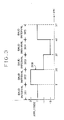
- FIG. 1 shows the use of the present invention within the transmitter of an illustrative communications system utilizing QAM modulation.
- bits of a digital data signal, on lead 140 are coupled through serial-to-parallel converter 141 to buses 111 and 113.
- Buses 111 and 113 each comprise a plurality of parallel conductors wherein the number of conductors in each bus varies with the modulation format being synthesized and, more specifically, is equal to the number of bits per digital symbol.
- buses 111 and 113 commonly referred to as the I rail and Q rail, respectively, each include 2 conductors since each modulated carrier signal conveys information on four discrete amplitude levels. Therefore, there are 2 bits per symbol on each rail.
- converter 141 spreads successive bits of the data signal on lead 140 across the combined total number of leads in buses 111 and 113.
- Each delay line clocked by the baud rate clock CLK, comprises a plurality of delay elements 112-1 through 112-N and 116-1 through 116-N. Each of these delay elements provide a delay of one baud or symbol interval T.
- Buses 115-1 through 115-N and 117-1 through 117-N respectively couple the delayed bits from delay lines 112 and 116 to memory 118 and form a predetermined portion of the memory address.
- this predetermined portion of the memory address comprises successive bits from buses 111 and 113 which represent a digital symbol from each bus and a number of digital symbols preceding and succeeding the digital symbol.
- converter 141 and delay lines 112 and 116 serve to arrange the data signals on lead 140 into overlapping portions each comprising M times N bits, where M is equal to the number of data bits per symbol per rail and N is equal to the number of tapped data symbols from each delay line.
- M equal to the number of data bits per symbol per rail
- N is equal to the number of tapped data symbols from each delay line.
- memory 118 For each random address generated by 112 and 116, memory 118 reads out onto bus 120 at least two digital representations. Each digital representation corresponds to a different sample of amplitude modulated quadrature-related carrier signals wherein the amplitude of each carrier has been modulated by a composite of specifically-shaped impulse time functions which are temporally displaced from one another and weighted by the successive digital symbols appearing on a different one of the buses 115 and 117.
- FIG. 2 shows a prior art 16 QAM modulator.
- the digital data signal on lead 220 is coupled to serial-to-parallel converter 221 which spreads successive bits of the data signal onto leads 231 through 234, respectively.
- Digital-to-analog (D/A) converter 222 quantizes signals appearing on leads 231 and 232 into a number of signal voltages which appear on lead 235.
- D/A converter 223 quantizes the signals on leads 233 and 234 into a number of signal voltages which are coupled to lead 236. For the case of 16 QAM modulation, 4 signal voltages appear on lead 235.
- Multipliers 227 and 228 receive the signal voltages on leads 235 and 236 after they are respectively smoothed by filters 224 and 225, which are typically half-Nyquist filters but could provide more arbitrary spectral shaping.
- Multiplier 227 modulates the amplitude of a carrier signal generated by oscillator 226 with the signals on lead 235 after filtering.
- multiplier 228 modulates the amplitude of a second carrier signal with the signals on lead 236 after smoothing by filter 225.
- the second carrier signal supplied to multiplier 228 is generated by shifting the carrier signal generated by oscillator 226 by minus ⁇ /2 radians via phase shifter 229.
- the pair of carrier signals supplied to multipliers 227 and 228 are in phase quadrature to one another and the products provided by multipliers 227 and 228 are each double-sideband signals.
- Summer 230 then adds the products provided by multipliers 227 and 228 and outputs this sum, also a double-sideband signal, onto lead 202.
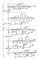
- FIG. 3 shows an illustrative time-varying waveform 300 appearing at the output of a typical D/A converter 222 or 223 of FIG. 2 for the 16 QAM system wherein the permissible transmitted symbols are ⁇ 1 and ⁇ 3 volts.
- the waveform has been idealized in the sense that the rise and fall times are non-existent.
- Waveform 300 has an amplitude that changes value randomly among the permissible transmitted symbols after each baud interval T. This randomness is indicated by waveform 300 having an amplitude of +1, +3, -1, -3, and +1 volts during baud intervals 301, 302, 303, 304 and 305, respectively.
- the spectrum of waveform 300 has the typical shape, where x is a well-known function of frequency.
- FIG. 4 shows the square pulse response 401 of an idealized half-Nyquist filter 224 or 225 of FIG. 2 including compensation, with the square impulse being the isolated portion of waveform 300 during baud interval 301.
- filter 224 or 225 has a signal propagation delay ⁇ and that the impulse response 401 to a band-limited digital symbol "rings out" or spreads forever in time.
- the maximum amplitude of response 401 is proportional to the amplitude of waveform 300 during the associated baud interval, i.e., baud interval 301, or, equivalently is proportional to the value of the associated digital symbol. This maximum amplitude is achieved a time interval ⁇ after the beginning of the associated baud interval.
- waveforms 410, 420, 430 and 440 show the responses of filter 224 or 225 to waveform 300 during baud intervals 302, 303, 304 and 305, respectively. Each of these responses extends forever in time and possesses the impulse response of FIG. 4 weighted by the associated data symbol. Accordingly, the maximum values of impulse responses 410, 420, 430 and 440 are respectively equal to +3, -1, -3, and +1 volts.
- the time-varying waveform on lead 237 or 238 of FIG. 2 during any baud interval is, therefore, theoretically equal to a composite of the filter impulse response from this baud interval and the filter impulse responses from all preceding and succeeding baud intervals.
- the signal synthesized by the embodiment of FIG. 1 is the sum of the composite function on leads 237 and 238 each multiplied by an associated carrier signal.
- This modulated signal designated as f(t)
- Signal f(t) is a double-sideband signal and has the frequency spectrum shown in FIG. 6.
- the synthesis of f(t) is achieved by respectively approximating a(t) and b(t) during any given baud interval by composite waveforms a ⁇ (t) and b ⁇ (t) where each composite waveform is an aggregation of weighted impulse response during the given baud interval and a predetermined, finite number of weighted impulse responses from adjacent baud intervals. Typically, these adjacent baud intervals are successive and immediately precede and succeed the given baud interval. This approximation provides a satisfactory result since the magnitude of the filter impulse response decays rapidly with time.
- lines 402 and 403 indicate the truncation of impulse response 401 some integer number of baud intervals, n, before and after the time 404 at which the absolute value of the amplitude is a maximum.
- times such as 404
- the truncation of response 401 is symmetric with respect to maximum amplitude time 404. However, this need not be so.
- each response could be truncated 5 baud intervals before and 3 baud intervals after time 404.
- the truncated response 401 extends over 2n baud intervals lying between lines 402 and 403 and is zero everywhere else.
- bus 115 supplies memory 118 with a set of N binary coded digital symbols used to form a ⁇ (t) for this baud interval and bus 117 supplies memory 118 with the other set of N binary coded digital symbols used to form b ⁇ (t).
- memory 118 reads out the value of a ⁇ (t)sin2 ⁇ f ⁇ c t + b ⁇ (t)cos2 ⁇ f ⁇ c t at two or more equally spaced times.
- f ⁇ c is restricted to be a rational multiple of the baud rate equal to or greater than 1/2 of the baud rate. This requirement that f ⁇ c be a rational multiple of the baud rate is necessary for digital synthesis, for without it, an infinite memory 118 is required.
- bit rate is an integer multiple of the baud rate for a maximum efficiency.
- the number of digital representations read out from memory 118 per baud interval must satisfy the Nyquist sampling theorem if f ⁇ (t) is to be reconstructed. For the present invention, this theorem is satisfied so long as the number of digital representations read out per baud interval is a rational multiple of the baud rate which avoids aliasing in the output signal frequency spectrum which is subsequently transmitted. This rational multiple is designated as J/K where J/K ⁇ Z, a number which varies with each application and which cannot be less than 2. We again shall assume that J/K is a reduced fraction, and that J and K are positive integers.
- the output signal of the present invention appears on lead 129 or, as will be discussed, appears on lead 125 in systems applications where multiplier 126 and band pass filter 128 are not required.
- Sampling counter 131 contributes the portion of each memory 118 address which determines the number of digital representations read out per baud interval. This portion appears on bus 134.
- Counter 131 is clocked by a clocking signal on bus 133 which is equal to J/K times the baud rate.
- Rational multiple clock generator 132 produces this clocking signal from the baud rate clock CLK.
- Counter 130 clocked by CLK, is required whenever ⁇ c is some non-integer, rational multiple P/R times CLK. As will be shown, there are R different digital representations for any set of digital symbols on buses 115 and 117, and, consequently, counter 130 counts from 1 to R and then resets.
- FIGs. 7 and 8 show how the digital representations stored in memory 118 are determined.
- the current digital symbols in baud interval 701 which appear as buses 111 and 113 are respectively designated as a0 and b0 with past and future symbols designated with negative and positive subscripts, respectively.
- the numerical values of the subscripts indicate the temporal proximity, in baud or symbol intervals, to the currently transmitted digital symbol.
- baud intervals 702 and 703, which are respectively one and two baud intervals after baud interval 701 the current digital symbols are respectively a1, b1 and a2, b2.
- Waveform a ⁇ (t) in FIG.7 illustrates the composite waveform formed by superimposing each baud interval with the 5 displaced, truncated impulse responses, each individually weighted by the 5 digital data symbols stored in delay line 112 during each baud interval.
- waveform b ⁇ (t) illustrates the composite waveform formed by repeating this aggregation process each baud interval for the digital symbols stored in delay line 116.
- memory unit 118 of FIG. 1 must store R different sets of digital representations of f ⁇ (t). Furthermore, since each digital representation corresponds to a sample of f ⁇ (t) in a baud interval, the number of digital representations in each set is equal to the number of sampling times for the baud interval.
- the selection of the particular set of digital representations is determined by the count of center frequency counter 130, while the count of counter 131 sequentially arranges the plurality of stored digital representations per set.
- the memory 118 location storing the digital representations of f ⁇ (t) at sampling times 705 and 706 has the addresses a -2 a -1 a0a +1 a +2 b -2 b -1 b0b +1 b +2 0000 and a -2 a -1 a0a +1 a +2 b -2 b -1 b0b +1 b +2 0010, where the 000 and 001 which precede the last bit positions indicate the count of sampling counter 131 and the 0 in the last bit position indicates the count of center frequency counter 130.
- sampling counter 131 would count from 0 to 6, whose binary representations are 000 and 110, respectively, and center frequency counter 130 would count from 0 to 1.
- the addresses for the digital representations of f ⁇ (t) at sampling times 712, 713, 719 and 720 respectively are a -1 a0a +1 a +2 a +3 b -1 b0b +1 b +2 b +3 0001, a -1 a0a +1 a +2 a +3 b -1 b0b +1 b +2 b +3 0011, a0a +1 a +2 a +3 a +4 b0b +1 b +2 b +3 b +4 0000, a0a +1 a +2 a +3 a +4 b0b0b +1 b +2 b +3 b +4 0000, a0a +1 a +2 a +3 a +4 b0b0b +1 b +2
- the digital representations read out of memory 118 appear on bus 120 and are coupled to D/A converter 121 which creates an analog waveform on lead 122.
- This analog waveform has the spectrum shown in FIG. 9, where f s is equal to the sampling frequency.
- Low pass filter 123 eliminates harmonics from this spectrum yielding a signal spectrum on lead 125 that is shown in FIG. 10.
- the frequency of the quadrature-related carrier signals is restricted to be a rational multiple of the baud rate. In certain applications, however, it may be desirable or necessary for the transmitted carrier frequency to be at some arbitrary frequency, f c , which is not a rational multiple of the baud rate.
- Band pass filter 128 is then utilized to eliminate the unwanted portion of the spectrum caused by the frequency translation and produce the spectrum shown in FIG. 6 and appearing on lead 129.
- the present invention can be used to synthesize the amplitude modulation of a single carrier by a data signal.
- the digital representations stored in memory 118 can be improved to compensate for in-rail and cross-rail distortions.
- the characteristic shape in the output signal from D/A converter 121 can be compensated for by pre-emphasizing the signal stored in memory 118 with . Such compensation can also be provided for a single amplitude modulated carrier signal.
- memory 118 comprises a single memory of R sections
- two memory units can be used, one storing a ⁇ (t)cos2 ⁇ f ⁇ c t and the other storing b ⁇ (t)sin2 ⁇ f ⁇ c t, along with a summer in lieu of memory 118.
Applications Claiming Priority (2)
| Application Number | Priority Date | Filing Date | Title |
|---|---|---|---|
| US06/892,232 US4736389A (en) | 1986-08-04 | 1986-08-04 | Technique for synthesizing the modulation of a time varying waveform with a data signal |
| US892232 | 1986-08-04 |
Publications (3)
| Publication Number | Publication Date |
|---|---|
| EP0256700A2 true EP0256700A2 (de) | 1988-02-24 |
| EP0256700A3 EP0256700A3 (en) | 1989-11-15 |
| EP0256700B1 EP0256700B1 (de) | 1995-09-20 |
Family
ID=25399604
Family Applications (1)
| Application Number | Title | Priority Date | Filing Date |
|---|---|---|---|
| EP87306677A Expired - Lifetime EP0256700B1 (de) | 1986-08-04 | 1987-07-29 | Anordnung zur Synthese der Modulation einer zeitveränderlichen Welle mit einem Datensignal |
Country Status (5)
| Country | Link |
|---|---|
| US (1) | US4736389A (de) |
| EP (1) | EP0256700B1 (de) |
| JP (1) | JPS63114341A (de) |
| CA (1) | CA1267195A (de) |
| DE (1) | DE3751526T2 (de) |
Cited By (3)
| Publication number | Priority date | Publication date | Assignee | Title |
|---|---|---|---|---|
| WO1992015165A1 (en) * | 1991-02-15 | 1992-09-03 | Schlumberger Technology Corporation | Transmission of well-logging data over bandpass channels using quadrature amplitude modulation |
| US5253271A (en) * | 1991-02-15 | 1993-10-12 | Schlumberger Technology Corporation | Method and apparatus for quadrature amplitude modulation of digital data using a finite state machine |
| US5661758A (en) * | 1996-01-16 | 1997-08-26 | Long; Michael E. | Single cycle data encoding method and apparatus |
Families Citing this family (8)
| Publication number | Priority date | Publication date | Assignee | Title |
|---|---|---|---|---|
| IL89461A (en) * | 1989-03-02 | 1994-06-24 | Eci Telecom Limited | Telephone communication compression system |
| KR930012023B1 (ko) * | 1991-01-25 | 1993-12-23 | 삼성전관 주식회사 | 평탄한 엔벨로프 특성을 갖는 bpsk 변조회로 |
| US5177455A (en) * | 1992-01-22 | 1993-01-05 | Mpr Teltech Ltd. | Digital phase and amplitude modulator |
| US5255269A (en) * | 1992-03-30 | 1993-10-19 | Spacecom Systems, Inc. | Transmission of data by frequency modulation using gray code |
| JPH06197084A (ja) * | 1992-12-25 | 1994-07-15 | Takayama:Kk | 音声転送方法 |
| JP2643762B2 (ja) * | 1993-04-12 | 1997-08-20 | 日本電気株式会社 | ディジタル化直交変調器 |
| DE19844457C1 (de) | 1998-09-28 | 2000-07-06 | Siemens Ag | Verfahren zur Duplex-Datenübertragung mit QAM und Demodulator zur Verwendung in diesem Verfahren |
| US7154431B2 (en) * | 1999-09-01 | 2006-12-26 | The United States Of America As Represented By The Secretary Of The Navy | Signal synthesizer and method therefor |
Citations (3)
| Publication number | Priority date | Publication date | Assignee | Title |
|---|---|---|---|---|
| US3988540A (en) * | 1972-05-05 | 1976-10-26 | Milgo Electronic Corporation | Integrated circuit modem with a memory storage device for generating a modulated carrier signal |
| FR2513462A1 (fr) * | 1981-09-21 | 1983-03-25 | Racal Data Communications Inc | Procede pour reduire l'encombrement d'une memoire d'un transmetteur et ce transmetteur |
| WO1986003356A1 (en) * | 1984-11-22 | 1986-06-05 | Devon County Council | Data modem system |
Family Cites Families (11)
| Publication number | Priority date | Publication date | Assignee | Title |
|---|---|---|---|---|
| US3763364A (en) * | 1971-11-26 | 1973-10-02 | North American Rockwell | Apparatus for storing and reading out periodic waveforms |
| JPS5375752A (en) * | 1976-12-16 | 1978-07-05 | Nec Corp | Data transmitter |
| US4327419A (en) * | 1980-02-22 | 1982-04-27 | Kawai Musical Instrument Mfg. Co., Ltd. | Digital noise generator for electronic musical instruments |
| NZ198844A (en) * | 1980-11-14 | 1984-05-31 | Plessey Overseas | Digital information transmission: two dimensional code |
| JPS5943144A (ja) * | 1982-09-02 | 1984-03-10 | 金井 宏之 | 軽量ヘルド |
| US4646326A (en) * | 1983-10-20 | 1987-02-24 | Motorola Inc. | QAM modulator circuit |
| US4599583A (en) * | 1983-11-19 | 1986-07-08 | Fujitsu Limited | Mixed dual frequency generating system |
| US4613976A (en) * | 1984-05-02 | 1986-09-23 | British Columbia Telephone Company | Constant envelope offset QPSK modulator |
| US4586023A (en) * | 1984-06-06 | 1986-04-29 | Motorola Information Systems Limited | Means and method for data transmission on wired channels |
| JP2510490B2 (ja) * | 1985-04-10 | 1996-06-26 | 株式会社日立製作所 | デイジタル変調器 |
| JPS6285538A (ja) * | 1985-10-11 | 1987-04-20 | Hitachi Ltd | デイジタル変調器 |
-
1986
- 1986-08-04 US US06/892,232 patent/US4736389A/en not_active Expired - Lifetime
-
1987
- 1987-07-21 CA CA000542612A patent/CA1267195A/en not_active Expired - Lifetime
- 1987-07-29 DE DE3751526T patent/DE3751526T2/de not_active Expired - Lifetime
- 1987-07-29 EP EP87306677A patent/EP0256700B1/de not_active Expired - Lifetime
- 1987-08-04 JP JP62193865A patent/JPS63114341A/ja active Granted
Patent Citations (3)
| Publication number | Priority date | Publication date | Assignee | Title |
|---|---|---|---|---|
| US3988540A (en) * | 1972-05-05 | 1976-10-26 | Milgo Electronic Corporation | Integrated circuit modem with a memory storage device for generating a modulated carrier signal |
| FR2513462A1 (fr) * | 1981-09-21 | 1983-03-25 | Racal Data Communications Inc | Procede pour reduire l'encombrement d'une memoire d'un transmetteur et ce transmetteur |
| WO1986003356A1 (en) * | 1984-11-22 | 1986-06-05 | Devon County Council | Data modem system |
Cited By (4)
| Publication number | Priority date | Publication date | Assignee | Title |
|---|---|---|---|---|
| WO1992015165A1 (en) * | 1991-02-15 | 1992-09-03 | Schlumberger Technology Corporation | Transmission of well-logging data over bandpass channels using quadrature amplitude modulation |
| US5253271A (en) * | 1991-02-15 | 1993-10-12 | Schlumberger Technology Corporation | Method and apparatus for quadrature amplitude modulation of digital data using a finite state machine |
| US5838727A (en) * | 1991-02-15 | 1998-11-17 | Schlumberger Technology Corporation | Method and apparatus for transmitting and receiving digital data over a bandpass channel |
| US5661758A (en) * | 1996-01-16 | 1997-08-26 | Long; Michael E. | Single cycle data encoding method and apparatus |
Also Published As
| Publication number | Publication date |
|---|---|
| JPS63114341A (ja) | 1988-05-19 |
| JPH0472425B2 (de) | 1992-11-18 |
| US4736389A (en) | 1988-04-05 |
| CA1267195A (en) | 1990-03-27 |
| EP0256700B1 (de) | 1995-09-20 |
| EP0256700A3 (en) | 1989-11-15 |
| DE3751526T2 (de) | 1996-05-09 |
| DE3751526D1 (de) | 1995-10-26 |
Similar Documents
| Publication | Publication Date | Title |
|---|---|---|
| US5487089A (en) | Nyquist filter for digital modulation | |
| EP0716785B1 (de) | Verbessertes rom filter | |
| EP0776110B1 (de) | Quadraturmodulationsschaltung | |
| JPH06188927A (ja) | ディジタル信号の送信方法及びそのための送信器 | |
| US4736389A (en) | Technique for synthesizing the modulation of a time varying waveform with a data signal | |
| US4710891A (en) | Digital synthesis technique for pulses having predetermined time and frequency domain characteristics | |
| US4812786A (en) | Method and system for providing precise multi-function modulation | |
| US6668013B1 (en) | Digital filter | |
| US7346125B2 (en) | Method and device for pulse shaping QPSK signals | |
| EP0577670A1 (de) | Rahmensynchronisierung für QAM | |
| EP0607896B1 (de) | Transversaler Filter geeignet zur Verarbeitung von Eingangssignalen mit hoher Datenrate | |
| US6870429B2 (en) | Variable rate modulator | |
| KR100743991B1 (ko) | 복소 변조기 반송파 신호 생성 장치 및 방법 | |
| US5832030A (en) | Multi-carrier transmission system utilizing channels with different error rates | |
| KR20020079794A (ko) | 감소된 검색 테이블을 사용하는 8-psk 전송 필터링 | |
| EP1223716B1 (de) | Wellenformerzeuger | |
| EP1079574A2 (de) | Digital VSB modulator | |
| US5177455A (en) | Digital phase and amplitude modulator | |
| JPH084277B2 (ja) | デジタル通信システム | |
| JP4743943B2 (ja) | パルスコード変調−dc中心vsb変換器 | |
| JPH06291790A (ja) | π/4シフトQPSK変調器 | |
| EP0220705B1 (de) | Vierphasiges Phasenmodulationssystem | |
| AU2002252711B2 (en) | Method and device for pulse shaping QPSK signals | |
| JPS59132267A (ja) | 多方向多重通信用子局送信装置のバ−スト状デ−タ信号波形整形回路 | |
| JP3357454B2 (ja) | ロールオフフィルタ及びこれに適する方法 |
Legal Events
| Date | Code | Title | Description |
|---|---|---|---|
| PUAI | Public reference made under article 153(3) epc to a published international application that has entered the european phase |
Free format text: ORIGINAL CODE: 0009012 |
|
| AK | Designated contracting states |
Kind code of ref document: A2 Designated state(s): DE FR GB IT |
|
| PUAL | Search report despatched |
Free format text: ORIGINAL CODE: 0009013 |
|
| AK | Designated contracting states |
Kind code of ref document: A3 Designated state(s): DE FR GB IT |
|
| 17P | Request for examination filed |
Effective date: 19900508 |
|
| 17Q | First examination report despatched |
Effective date: 19920312 |
|
| RAP3 | Party data changed (applicant data changed or rights of an application transferred) |
Owner name: AT&T CORP. |
|
| GRAA | (expected) grant |
Free format text: ORIGINAL CODE: 0009210 |
|
| AK | Designated contracting states |
Kind code of ref document: B1 Designated state(s): DE FR GB IT |
|
| REF | Corresponds to: |
Ref document number: 3751526 Country of ref document: DE Date of ref document: 19951026 |
|
| ET | Fr: translation filed | ||
| ITF | It: translation for a ep patent filed |
Owner name: MODIANO & ASSOCIATI S.R.L. |
|
| PLBE | No opposition filed within time limit |
Free format text: ORIGINAL CODE: 0009261 |
|
| STAA | Information on the status of an ep patent application or granted ep patent |
Free format text: STATUS: NO OPPOSITION FILED WITHIN TIME LIMIT |
|
| 26N | No opposition filed | ||
| REG | Reference to a national code |
Ref country code: GB Ref legal event code: IF02 |
|
| PGFP | Annual fee paid to national office [announced via postgrant information from national office to epo] |
Ref country code: DE Payment date: 20060714 Year of fee payment: 20 Ref country code: FR Payment date: 20060714 Year of fee payment: 20 |
|
| PGFP | Annual fee paid to national office [announced via postgrant information from national office to epo] |
Ref country code: GB Payment date: 20060720 Year of fee payment: 20 |
|
| PGFP | Annual fee paid to national office [announced via postgrant information from national office to epo] |
Ref country code: IT Payment date: 20060731 Year of fee payment: 20 |
|
| REG | Reference to a national code |
Ref country code: GB Ref legal event code: PE20 |
|
| PG25 | Lapsed in a contracting state [announced via postgrant information from national office to epo] |
Ref country code: GB Free format text: LAPSE BECAUSE OF EXPIRATION OF PROTECTION Effective date: 20070728 |