US4599583A - Mixed dual frequency generating system - Google Patents

Mixed dual frequency generating system Download PDF

Info

Publication number
US4599583A
US4599583A US06/671,775 US67177584A US4599583A US 4599583 A US4599583 A US 4599583A US 67177584 A US67177584 A US 67177584A US 4599583 A US4599583 A US 4599583A
Authority
US
United States
Prior art keywords
extracting
extracting address
address
data
control signal
Prior art date
Legal status (The legal status is an assumption and is not a legal conclusion. Google has not performed a legal analysis and makes no representation as to the accuracy of the status listed.)
Expired - Fee Related
Application number
US06/671,775
Inventor
Ryoji Shimozono
Yasunori Ogawa
Yasuo Tanaka
Shigeo Sano
Current Assignee (The listed assignees may be inaccurate. Google has not performed a legal analysis and makes no representation or warranty as to the accuracy of the list.)
Fujitsu Ltd
Original Assignee
Fujitsu Ltd
Priority date (The priority date is an assumption and is not a legal conclusion. Google has not performed a legal analysis and makes no representation as to the accuracy of the date listed.)
Filing date
Publication date
Priority claimed from JP21710183A external-priority patent/JPS60109907A/en
Priority claimed from JP22100983A external-priority patent/JPS60113556A/en
Application filed by Fujitsu Ltd filed Critical Fujitsu Ltd
Assigned to FUJITSU LIMITED reassignment FUJITSU LIMITED ASSIGNMENT OF ASSIGNORS INTEREST. Assignors: OGAWA, YASUNORI, SANO, SHIGEO, SHIMOZONO, RYOJI, TANAKA, YASUO
Application granted granted Critical
Publication of US4599583A publication Critical patent/US4599583A/en
Anticipated expiration legal-status Critical
Expired - Fee Related legal-status Critical Current

Links

Images

Classifications

    • HELECTRICITY
    • H04ELECTRIC COMMUNICATION TECHNIQUE
    • H04LTRANSMISSION OF DIGITAL INFORMATION, e.g. TELEGRAPHIC COMMUNICATION
    • H04L27/00Modulated-carrier systems
    • H04L27/18Phase-modulated carrier systems, i.e. using phase-shift keying
    • H04L27/20Modulator circuits; Transmitter circuits
    • H04L27/2003Modulator circuits; Transmitter circuits for continuous phase modulation
    • H04L27/2007Modulator circuits; Transmitter circuits for continuous phase modulation in which the phase change within each symbol period is constrained
    • H04L27/2014Modulator circuits; Transmitter circuits for continuous phase modulation in which the phase change within each symbol period is constrained in which the phase changes in a piecewise linear manner during each symbol period, e.g. minimum shift keying, fast frequency shift keying

Definitions

  • the present invention relates to a mixed dual frequency generating system for outputting a digital signal having, when converted into an analog signal, a desired frequency or frequencies.
  • a mixed dual frequency generating system for providing a digital frequency-shift keying (FSK) signal or for providing a digital signal having, when converted into an analog signal, two mixed frequencies.
  • FSK digital frequency-shift keying
  • the transmission of analog FSK signal is disclosed in, for example, U.S. Pat. No. 4,368,439.
  • the digital FSK signal consists of a sequence of binary coded signals expressing a logic "1" and a logic "0".
  • Each of the binary coded signals in the digital FSK signal consists of a PCM signal obtained by sampling a sine wave.
  • the logic "1" in the digital FSK signal is formed by a PCM signal having, when converted into an analog signal, a first frequency
  • the logic "0" in the digital FSK signal is formed by a PCM signal having, when converted into an analog signal, a second frequency, different from the first frequency.
  • the two frequencies are 980 Hz and 1180 Hz, respectively.
  • two PCM signal sources are employed for generating the above-mentioned two PCM signals. These two PCM signals are always generated from the two PCM signal sources, and a selection unit switches from one of the two PCM signals to the other PCM signal to be output from the device.
  • a device for generating two mixed signals having different frequencies is useful for various applications. For example, in an examination of a modem, by applying a signal having two mixed frequencies, the characteristics for respective frequency components can be simultaneously examined. Also, a tone signal composed of two mixed frequencies is often used.
  • a conventional technique is to provide two oscillators respectively generating frequencies different from each other. In this conventional case also, the need for two oscillators makes the device expensive.
  • a read only memory may be used to obtain two signals having different frequencies by storing mixed data obtained by sampling two sine waves having different frequencies. By sequentially reading the ROM with a sampling period the mixed data can be read. In this case, however, it is impossible to change the frequencies of the output two signals because the stored mixed data are fixed data and are read step by step sequentially. Also, because the ROM must store mixed data for two different frequencies, the memory size of the ROM must be large.
  • An object of the present invention is to provide a digital signal generating device which can generate a digital FSK signal with no discontinuity in phase and amplitude.
  • Another object of the present invention is to provide a digital FSK signal generating device which can change the frequency of the output without a discontinuity in the phase of the PCM signal, thereby decreasing the possibility of erroneous detection at the receiving side.
  • Still another object of the present invention is to provide a mixed dual frequency generating system which can output two mixed signals having different frequencies without using two oscillators, but instead, using only a single ROM.
  • a still further object of the present invention is to provide a mixed dual frequency generating system which can output two mixed signals having different frequencies, and in which the frequencies are easily changed.
  • a mixed dual frequency generating system comprising sampled data storing means for sequentially storing, in its continuous addresses, a plurality of digital sampled data obtained by sampling, with a predetermined sampling frequency, a fundamental sine wave having a fundamental frequency; extracting step number storing means for storing at least one extracting step number; and data extracting means for extracting, with the predetermined sampled frequency, a part of the digital sampled data from the sampled data storing means by accessing extracting addresses in the continuous addresses of the sampled data storing means.
  • the extracting addresses are determined in such a way as to add the extracting step number to a previous extracting address to form a new extracting address.
  • the sampled data storing means stores data indicating a predetermined cycle portion of the fundamental sine wave. This predetermined cycle portion is at least equal to one quarter of one cycle of the fundamental sine wave.
  • the data extracting means comprises an extracting address latching means, and an extracting address calculating means.
  • the extracting address latching means operatively latches the previous extracting address until a first new extracting address is determined.
  • the extracting address calculating means operatively calculates the first new extracting address by adding the extracting step number to the previous extracting address output from the extracting address latching means.
  • the predetermined cycle portion is equal to, for example, a half cycle or even one cycle of the fundamental sine wave.
  • the device further comprises a control means for providing, when the first new extracting address is greater than or equal to the number of sampling steps in one cycle, a first control signal to the calculating means.
  • the calculating means operatively calculates, in response to the first control signal, a second new extracting address by subtracting the number of sampling steps in one cycle from the first new extracting address.
  • the extracting address latching means operatively updates the previous extracting address by the first new extracting address when the first control signal is not applied to the calculating means or by the second new extracting address when the first control signal is applied to the calculating means.
  • the device further comprises means for changing every alternate first new extracting address to a predetermined extracting address.
  • the predetermined address of the sampled data storing means the data "0" is stored.
  • FIG. 1 is a waveform diagram for explaining a well-known FSK signal
  • FIG. 2 is a block diagram of a well-known telephone-communication line system employing PCM channels for which the present invention is applicable.
  • FIG. 3 is a block diagram of an example of a conventional digital FSK signal generating device.
  • FIG. 4 is a waveform diagram for explaining the problems in the conventional device
  • FIG. 5 is a block diagram of a digital FSK signal generating device, according to a first embodiment of the present invention.
  • FIG. 6 is a plurality of digital sampled data obtained from a fundamental sine wave over one cycle
  • FIG. 7 is a flowchart explaining the operation of the device shown in FIG. 5;
  • FIG. 8 is a graph of an example of the digital FSK signal extracted from the device shown in FIG. 5;
  • FIG. 9 is a graph of the digital sampled data obtained from a 1/4 cycle of the fundamental sine wave
  • FIG. 10 is a block diagram of a digital FSK signal generating device according to a second embodiment of the present invention.
  • FIG. 11 is a flowchart explaining the operation of the device shown in FIG. 10;
  • FIG. 12 is a block diagram illustrating a digital signal generating device according to a third embodiment of the present invention.
  • FIG. 13A is a waveform diagram illustrating a sine wave obtained from the device shown in FIG. 12;
  • FIG. 13B is a waveform diagram illustrating an analog signal including two frequencies which are also obtained from the device shown in FIG. 12;
  • FIG. 14 is a graph of a frequency spectrum of the two signals included in the analog signal shown in FIG. 13B;
  • FIG. 15 is a diagram explaining the operation of the device shown in FIG. 12.
  • FIG. 16 is a block diagram of a digital signal generating device according to a fourth embodiment of the present invention.
  • FIGS. 1 through 4 Before describing the embodiments of the present invention, the background of the invention and the prior art and problems therein will first be described with reference to FIGS. 1 through 4.
  • FIG. 1 shows a waveform diagram for explaining a well known FSK signal.
  • the FSK signal consists of a sequence of logical states, "1" and "0", of digital data to be sent.
  • Each of the logical states of "1” consists, when the FSK signal is formed by PCM signals, of sampled data which has, when converted into an analog sine wave, a first frequency fa equal to 980 Hz in this example.
  • each of the logical states "0" in the digital FSK signal consists of sampled data having a second frequency fz equal to 1180 Hz in this example.
  • the term "the frequency of the digital sampled data” will refer to the frequency of the sine wave corresponding to the digital sampled data.
  • FIG. 2 is a block diagram of a well-known telephone-communication line system employing PCM channels for which the present invention can be applied, and through which PCM channels the above-mentioned digital FSK signal is transmitted.
  • a modulator-demodulator (MODEM) 1 in a toll switching system 2 should preferably generate a PCM signal such as the above-mentioned digital FSK signal, rather than the analog FSK signal.
  • the modem 1 provides a digital FSK signal to a toll switch 3.
  • the toll switch 3 selects a digital terminal 4 to transmit the digital FSK signal through a PCM line 5 to a digital terminal 6 at a local switching system 7.
  • the digital FSK signal from the digital terminal 6 is time division switched by a local switch 8.
  • the output of the local switch 8 is converted into an analog signal by a coder-decoder (CODEC) 9.
  • CDDEC coder-decoder
  • the analog signal is then applied to a subscriber 10.
  • the system shown in FIG. 2 is applied to, for example, a detailed charging system for general telephone services in a hotel.
  • the digital FSK signal on the PCM line 5 is transmitted at a low speed of 300 baud.
  • FIG. 3 is a block diagram of an example of a conventional digital FSK signal generating device used in the prior art.
  • a selecting unit (SEL) 30 selects, in response to a logical state of a command C consisting of a binary code applied to an input terminal (IT) 31, one of two PCM signals generated by two signal sources (SGa) 32 and (SGz) 33.
  • the signal source (SGa) 32 always generates a PCM signal having a frequency fa, and the signal source SGz 33 always generates a PCM signal having a frequency fz.
  • the selected PCM signal is output from an output terminal (OT) 34.
  • OT output terminal
  • the conventional device since the conventional device includes the two signal sources (SGa) 32 and (SGz) 33, it has a disadvantage in that it is too expensive, and further, since the phases of the two signals generated by the two signal sources 32 and 33 do not always coincide, the digital FSK signal includes, at its switching points from "0" to "1” or from "1" to "0", impulse noises. This will be explained in more detail with reference to FIG. 4.
  • the wave forms S 1 and S 2 are discontinuous between the time t 0 and the time t 1 .
  • This discontinuity causes impulse noise at the receiver side, such as the subscriber 10 shown in FIG. 2.
  • FIG. 5 is a block diagram of a digital FSK signal generating device, according to a first embodiment of the present invention.
  • a sampled data storing unit (SD) 51 is a read only memory (ROM) for sequentially storing, in its continuous addresses, a plurality of digital sampled data. These digital sampled data are obtained by sampling a fundamental sine wave for a predetermined cycle portion.
  • the fundamental sine wave has a fundamental frequency f 0 which is a common measure or common divisor, as understood in mathematical terminology, of the two frequencies fa and fz in the desired digital FSK signal.
  • the frequencies fa and fz of the digital FSK signal are 980 Hz and 1180 Hz, respectively, a common measure of, for example, 2.5 Hz, is selected as the fundamental frequency f 0 of the fundamental sine wave.
  • the fundamental frequency f 0 may, of course, be another common measure such as 10 Hz, 20 Hz, etc.
  • the sampling frequency f of the PCM signal in a telephone switching system is usually equal to 8 kHz which is twice the maximum voice frequency.
  • the predetermined cycle portion is equal to one cycle C 0 of the fundamental sine wave.
  • the SD 51 in FIG. 5 stores one cycle C 0 of the fundamental sine wave.
  • FIG. 6 is a graph of a plurality of digital sampled data obtained from the fundamental sine wave for one cycle C 0 .
  • the fundamental sine wave FS has a fundamental frequency f 0 of 2.5 Hz.
  • the sampling frequency f is 8 kHz. Therefore, the number of sampling steps in the one cycle C 0 of the sine wave FS is equal to f/f 0 , i.e., 3200 steps. Also, the sampling period is 1/8000 second, i.e., 125 ⁇ s.
  • Sampled values D 0 , D 1 , D 2 , D 3 , . . . , and D 3199 obtained by the sampling are stored sequentially as the digital sampled data in the sampled data storing unit (SD) 51 shown in FIG. 5.
  • SD sampled data storing unit
  • the digital FSK signal generating device further includes an extracting step number storing unit (EN) 52, an extracting address calculating unit (ALU) 53, an extracting address latching unit (ADL) 54, and a control unit (CTL) 55.
  • EN extracting step number storing unit
  • ALU extracting address calculating unit
  • ADL extracting address latching unit
  • CTL control unit
  • FIG. 7 is a flowchart explaining the operation of the device shown in FIG. 5.
  • the CTL 55 discriminates whether the command C applied to the input terminal (IT) 56 is a command "a” or "z” for specifying the first frequency fa or the second frequency fz to be output.
  • the commands "a” and “z” are, for example, "1” and "0", respectively which are equal to the binary data to be sent from the device shown in FIG. 5 to the receiver.
  • the CTL 55 provides a control signal C 1a to the EN 52 which, at step S 2 , outputs the first extracting step number d 1a as the extracting step number d 1 , in response to the control signal C 1a . If the command C is the command "z”, the CTL 55 provides a control signal C 1z and the EN 52 outputs, at step S 3 , the second extracting step number d 1z as the extracting step number d 1 .
  • the ALU 53 calculates a next extracting address d 2 by adding the extracting step number d 1 with a previous extracting address d 3 which has been latched in the ADL 54.
  • the CTL 55 discriminates whether the calculated extracting address d 2 output from the ALU 53 is greater than or equal to the number of sampling steps in the one cycle, i.e., the number of sampling steps in this embodiment is 3200.
  • step S 6 the CTL 55 provides another control signal C 2 to the ALU 53, and the ALU 53 converts the extracting address d 2 into another new extracting address by subtracting the number of sampling steps (3200) from the new extracting address d 2 . That is, d 2 is updated to d 2 -3200.
  • step S 6 or if d 2 ⁇ 3200 at step S 5 , then the CTL 55 provides still another control signal C 3 to the ADL 54 so that, at step S 7 , the ADL 54 latches the updated or original new extracting address d 2 .
  • the previous extracting address d 3 is updated to the updated or original new extracting address d 2 , to form a current extracting address d 3 which is equal to d 2 .
  • step S 8 the SD 51 is accessed by the current extracting address d 3 so that a sampled data D i stored in the address d 3 of the SD 51 is read and output.
  • step S 9 the CTL 55 discriminates whether the transmission from the SD 51 should be ended. Until the transmission ends, the above mentioned steps S 1 through S 8 are repeated with the sampling frequency of 8 kHz. As a result, a digital FSK signal is obtained at the output terminal (OTa) 57.
  • FIG. 8 is a graph of an example of the digital FSK signal extracted from the SD 51 shown in FIG. 5.
  • data D 1a , D 9a , D 3a , . . . , and D 4a are those extracted from the SD 51 when the extracting step number is d 1a equal to 392.
  • the extracting address 3528 for extracting the data D 9a is greater than 3200. Therefore, the address 3528 is converted into 3528-3200, i.e., 328.
  • data D 1z , D 2z , D 3z , . . . are those extracted from the SD 51 when the extracting step number is d 1z which is equal to 472.
  • each of the extracting addresses for extracting the data D 1z , D 2z , . . . is calculated by adding the extracting step number 472 to the previous extracting address.
  • the PCM signal has the first frequency fa equal to 980 Hz, corresponding to, for example, "1" of the binary data and in the digital FSK signal to be sent to the receiver.
  • the term "digital" in the digital FSK signal does not relate to the binary data but relates to the PCM signal.
  • FIG. 9 shows the digital sampled data obtained from a 1/4 cycle of the fundamental sine wave FS.
  • 801 data samples D 0 , D 1 , D 2 , D 3 , . . . , and D 800 are obtained from the first 1/4 cycle of the fundamental sine wave FS.
  • the sampling period for obtaining the data samples D 0 , D 1 , . . . , and D 800 is the same as that shown in FIG. 6, i.e., 125 ⁇ s.
  • FIG. 10 is a block diagram of a digital FSK signal generating device according to a second embodiment of the present invention.
  • the device comprises a sampled data storing unit (SD) 51a, an extracting number storing unit (EN) 52a, an extracting address calculating unit (ALU) 53a, an extracting address latching unit (ADL) 54a, and a control unit (CTL) 55a, which are similar to those shown in FIG. 5 of the first embodiment.
  • SD sampled data storing unit
  • EN extracting number storing unit
  • ALU extracting address calculating unit
  • ADL extracting address latching unit
  • CTL control unit
  • the SD 51a stores the sampled data D 0 , D 1 , D 2 , . . . , and D 800 obtained from the first 1/4 cycle of the fundamental sine wave FS shown in FIG. 9. Because of this, the operation of the device shown in FIG. 10 is slightly different from that of the first embodiment.
  • FIG. 11 is a flowchart explaining the operation of the device shown in FIG. 10.
  • steps S 1a through S 4a are the same as the steps S 1 through S 4 shown in FIG. 7.
  • the CTL 55a discriminates whether the calculated extracting address d 2 is greater than or equal to the number of sampling steps in the 1/4 cycle (C 0 /4), i.e., whether d 2 is at a phase more than ⁇ /2.
  • step S 6a the CTL 55a provides a control signal C 2a to the ALU 53a, which then converts the extracting address d 2 into another new extracting address by calculating 1600-d 2 . Also, in response to the control signal C 2a , the ALU 53a inverts the sign of the extracting step number d 1 output from the EN 52a.
  • step S 6a the CTL 55 discriminates, at step S 7a , whether the calculated extracting address d 2 is equal to or smaller than zero.
  • step S 8a the CTL 55a provides still another control signal C 3a to the ADL 54a.
  • the ADL 54a inverts the sign of the thus calculated extracting address d 2 and latches it as an extracting address d 3 .
  • the CTL 55a provides a still further control signal C 4 to the ALU 53a, which then inverts the sign of the extracting step number d 1 .
  • step S 10a the ADL 54a latches the thus calculated extracting address d 2 as the extracting address d 3 , and outputs the noninverted sign code d 4 .
  • the SD 51a is accessed by the extracting address d 3 so that a sampled data D i stored in the address d 3 is output from the SD 51a to an output terminal OT b1 .
  • the sign code d 4 is output from the ADL 54a to another output terminal OT b2 .
  • the data (Di ⁇ d 4 ) is output from the device shown in FIG. 10.
  • steps S 1a through S 11a are repeated with the sampling frequency of 8 kHz until transmission end is detected by the CTL 55a at step 12a.
  • the frequency of the digital FSK signal is changed by changing the extracting step number, the phases of the PCM signals or analog signals obtained from the PCM signals are not discontinuous. Therefore, at a receiver, the digital FSK signal is received with decreased noise or with no error.
  • FIG. 12 is a block diagram illustrating a mixed dual frequency generating system 120 according to a third embodiment of the present invention.
  • the device shown in FIG. 12 is for generating a digital signal which has, when converted into an analog signal, two mixed frequencies.
  • the mixed dual frequency generating system 120 comprises an SD 51b, an EN 52b, an ALU 53b, an ADL 54b, and a CTL 55b which are similar to those shown in FIG. 10.
  • the output of the SD 51b is connected to a D/A converter 56.
  • the main differences from the second embodiment are that, in FIG.
  • the EN 52b stores only a single extracting step number d 1 , and that the CTL 55b controls the ADL 54b so that the ADL 54b outputs a fixed address alternately as an output address d 3a .
  • the data "0" is stored in the fixed address of the SD 51b.
  • the data "0" is output at alternate outputs.
  • the D/A converter 56 converts the digital data including "0" in alternate data, the analog signal obtained at the output of the D/A converter 56 includes two frequencies.
  • the SD 51b stores sampled data D 1b , D 2b , D 3b , . . . obtained from the first 1/4 cycle of a sine wave having a frequency f 0 , as shown in FIG. 9.
  • the sampled data D 1b , D 2b , D 3b , . . . are sequentially read, with the extracting step number d 1 , from the SD 51b in a way similar to that mentioned with reference to FIG.
  • the D/A converter converts the digital data D 1b , "0", D 3b , "0", D 5b , "0", . . . into an analog signal SW B , as shown in FIG. 13B.
  • the analog signal SW B contains two frequencies f 1 and f 2 .
  • the sampling frequency f is 8 kHz
  • the two frequencies f 1 and f 2 are f 0 ⁇ d 1 and 4 kHz-f 0 ⁇ d 1 .
  • the fundamental frequency f 0 of the fundamental sine wave is 2.5 Hz
  • the extracting step number d 1 is 500
  • the two frequencies are 1250 Hz and 2750 Hz.
  • FIG. 14 shows a frequency spectrum of the two signals included in the analog signal SW B .
  • n is an even number
  • the operation of the device 120 is almost the same as the operation of the device shown in FIG. 10. Therefore, the control signals C 2a , C 3a , and C 4 , and the extracting addresses d 2 and d 3 , are the same as those in FIG. 10.
  • the differences between the devices in FIGS. 10 and 12 are that, in FIG. 12, the EN 52b is not controlled by the CTL 55b but provides the predetermined single extracting step number d 1 , and that the CTL 55b provides a still further control signal C 5 to the ALU 53b and to the ADL 54b for every other output of the calculated extracting address d 2 .
  • FIG. 15 is a diagram explaining the operation of the device shown in FIG. 12.
  • the SD 51b outputs digital data D 0c , D 1c , D 2c , . . . at times t 0 , t 1 , t 2 , . . . , respectively.
  • Alternate data D 1c , D 3c , D 5c , . . . are "0".
  • the extracting period is equal to the sampling period, i.e., 125 ⁇ s.
  • the extracting number d 1 is assumed to be 300.
  • the control signal C 5 becomes "1" at alternate times t 0 , t 2 , t 4 , t 6 , . . . .
  • the extracting address d 3a output from the ADL 54b is made to be zero at alternate times t 0 , t 2 , t 4 , t 6 , . . . .
  • the control signal C 4 is turned from "0" to "1" when the calculated address d.sub. 2 output from ALU 53b becomes greater than the number of sampling steps in the range between 0 and ⁇ /2 in phase, i.e., when d 2 becomes greater than 800.
  • the control signal C 4 is turned from “1” to “0” when d 2 becomes negative, and the control signal C 3a is turned from “0” to “1” when the control signal C 4 changes its logic level, and the "1" level of the control signal C 3a continues for the sampling period of 125 ⁇ s.
  • the level of the sign code d 4 changes when the control signal C 4 changes from “1" to "0".
  • d 2 and d 3 are both preset values equal to zero in this example. Since C 5 is "1", d 3a for accessing the SD 51b is zero.
  • the extracting addresses d 2 , d 3 , and d 3a can be calculated in a way similar to the above.
  • the extracting step number d 1 can be arbitrarily set in the EN 52b. Also, the sampling frequency f can be arbitrarily selected. Therefore, the two frequencies f 0 ⁇ d 1 and f/2-f 0 ⁇ d 1 can be arbitrarily changed.
  • FIG. 16 is a block diagram of a mixed dual frequency generating system 160 according to a fourth embodiment of the present invention.
  • the mixed dual frequency generating system 160 shown in FIG. 16 is very similar to the device 120 shown in FIG. 12.
  • the same portions, signals, and extracting addresses are represented by the same reference symbols in both FIGS. 12 and 16.
  • the differences between FIGS. 12 and 16 are that, instead of accessing the address zero in alternate accessing timings, the device shown in FIG. 16 has a data storing unit (DS) 57 for storing the fixed data "0", and a switching circuit 58 for selecting the output of the SD 51c, or the output of the DS 57, in response to the control signal C 5 which turns to "1" at alternate extracting timings, as shown in FIG. 15.
  • the device shown in FIG. 16 can also provide a digital signal including the arbitrarily determined two frequencies f 0 ⁇ d 1 and f/2-f 0 ⁇ d 1 .
  • an address generating unit for generating the fixed address for accessing the "0" data may be provided between the ADL 54b and the SD 51b so that, instead of the fixed address from the ADL 54b, the fixed address from the address generating unit may be applied to the SD 51b.
  • a digital signal generating device can generate a digital FSK signal with no discontinuity in phase and amplitude. Therefore, at a receiving side, the digital FSK signal is received with decreased noise and with a decrease in the number of errors detected.
  • the digital signal generating device can output two mixed digital signals from a single ROM so that the cost of the device is decreased in comparison with the conventional device employing two oscillators.
  • the frequency of the digital FSK signal or the frequencies of the two mixed frequencies can be easily changed.
  • the present invention is advantageous in, for example, telephone-communication line systems employing PCM channels.

Abstract

A mixed dual frequency generating system for generating a digital FSK signal or a signal including two mixed frequencies includes a ROM which stores in consecutive addresses sampled data obtained by sampling a sine wave at a sampling frequency. The mixed dual frequency generating system also includes a data extracting circuit for extracting the sampled data from the ROM at the sampling frequency using an extracting step number. An output data fixing circuit changes alternate data extracted from the ROM to data "O", so that a signal having two mixed frequencies can be obtained.

Description

BACKGROUND OF THE INVENTION
(1) Field of the Invention
The present invention relates to a mixed dual frequency generating system for outputting a digital signal having, when converted into an analog signal, a desired frequency or frequencies. In particular, it relates to a mixed dual frequency generating system for providing a digital frequency-shift keying (FSK) signal or for providing a digital signal having, when converted into an analog signal, two mixed frequencies.
(2) Description of the Related Art
The transmission of analog FSK signal is disclosed in, for example, U.S. Pat. No. 4,368,439. In the field of telephone-line systems, however, wide use is made of PCM channels through which a so-called digital FSK signal is transmitted. The digital FSK signal consists of a sequence of binary coded signals expressing a logic "1" and a logic "0". Each of the binary coded signals in the digital FSK signal consists of a PCM signal obtained by sampling a sine wave. That is, the logic "1" in the digital FSK signal is formed by a PCM signal having, when converted into an analog signal, a first frequency, and the logic "0" in the digital FSK signal is formed by a PCM signal having, when converted into an analog signal, a second frequency, different from the first frequency. For example, according to CCITT, V21, the two frequencies are 980 Hz and 1180 Hz, respectively.
In a conventional digital FSK signal generating device, two PCM signal sources are employed for generating the above-mentioned two PCM signals. These two PCM signals are always generated from the two PCM signal sources, and a selection unit switches from one of the two PCM signals to the other PCM signal to be output from the device.
There are, however, disadvantages in the above conventional digital FSK signal generating device. That is, it needs two independent PCM signal sources, making it expensive, and at a switching point, these two PCM signals are not always in the same phase. Therefore, at the switching point, the phases of the PCM signals, or analog signals obtained from the PCM signal, usually become discontinuous, as later described in more detail. Because of this discontinuity, the digital FSK signal at the switching point has an impulse noise and, therefore, may be erroneously received at a receiver as noise or as another error signal.
Apart from the digital FSK signal generating device, a device for generating two mixed signals having different frequencies is useful for various applications. For example, in an examination of a modem, by applying a signal having two mixed frequencies, the characteristics for respective frequency components can be simultaneously examined. Also, a tone signal composed of two mixed frequencies is often used.
In order to generate such a signal having two mixed frequencies, a conventional technique is to provide two oscillators respectively generating frequencies different from each other. In this conventional case also, the need for two oscillators makes the device expensive.
A read only memory (ROM) may be used to obtain two signals having different frequencies by storing mixed data obtained by sampling two sine waves having different frequencies. By sequentially reading the ROM with a sampling period the mixed data can be read. In this case, however, it is impossible to change the frequencies of the output two signals because the stored mixed data are fixed data and are read step by step sequentially. Also, because the ROM must store mixed data for two different frequencies, the memory size of the ROM must be large.
SUMMARY OF THE INVENTION
An object of the present invention is to provide a digital signal generating device which can generate a digital FSK signal with no discontinuity in phase and amplitude.
Another object of the present invention is to provide a digital FSK signal generating device which can change the frequency of the output without a discontinuity in the phase of the PCM signal, thereby decreasing the possibility of erroneous detection at the receiving side.
Still another object of the present invention is to provide a mixed dual frequency generating system which can output two mixed signals having different frequencies without using two oscillators, but instead, using only a single ROM.
A still further object of the present invention is to provide a mixed dual frequency generating system which can output two mixed signals having different frequencies, and in which the frequencies are easily changed.
To achieve the above objects, there is provided, according to the present invention, a mixed dual frequency generating system comprising sampled data storing means for sequentially storing, in its continuous addresses, a plurality of digital sampled data obtained by sampling, with a predetermined sampling frequency, a fundamental sine wave having a fundamental frequency; extracting step number storing means for storing at least one extracting step number; and data extracting means for extracting, with the predetermined sampled frequency, a part of the digital sampled data from the sampled data storing means by accessing extracting addresses in the continuous addresses of the sampled data storing means. The extracting addresses are determined in such a way as to add the extracting step number to a previous extracting address to form a new extracting address.
The sampled data storing means stores data indicating a predetermined cycle portion of the fundamental sine wave. This predetermined cycle portion is at least equal to one quarter of one cycle of the fundamental sine wave.
The data extracting means comprises an extracting address latching means, and an extracting address calculating means.
The extracting address latching means operatively latches the previous extracting address until a first new extracting address is determined.
The extracting address calculating means operatively calculates the first new extracting address by adding the extracting step number to the previous extracting address output from the extracting address latching means.
According to one aspect of the present invention, the predetermined cycle portion is equal to, for example, a half cycle or even one cycle of the fundamental sine wave.
The device further comprises a control means for providing, when the first new extracting address is greater than or equal to the number of sampling steps in one cycle, a first control signal to the calculating means. The calculating means operatively calculates, in response to the first control signal, a second new extracting address by subtracting the number of sampling steps in one cycle from the first new extracting address.
The extracting address latching means operatively updates the previous extracting address by the first new extracting address when the first control signal is not applied to the calculating means or by the second new extracting address when the first control signal is applied to the calculating means.
According to another aspect of the present invention, the device further comprises means for changing every alternate first new extracting address to a predetermined extracting address. In the predetermined address of the sampled data storing means, the data "0" is stored.
BRIEF DESCRIPTION OF THE DRAWINGS
The above objects and features of the present invention will be more apparent from the following description of the preferred embodiments with reference to the accompanying drawings, wherein:
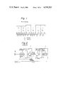
FIG. 1 is a waveform diagram for explaining a well-known FSK signal;
FIG. 2 is a block diagram of a well-known telephone-communication line system employing PCM channels for which the present invention is applicable.
FIG. 3 is a block diagram of an example of a conventional digital FSK signal generating device.
FIG. 4 is a waveform diagram for explaining the problems in the conventional device;
FIG. 5 is a block diagram of a digital FSK signal generating device, according to a first embodiment of the present invention;
FIG. 6 is a plurality of digital sampled data obtained from a fundamental sine wave over one cycle;
FIG. 7 is a flowchart explaining the operation of the device shown in FIG. 5;
FIG. 8 is a graph of an example of the digital FSK signal extracted from the device shown in FIG. 5;
FIG. 9 is a graph of the digital sampled data obtained from a 1/4 cycle of the fundamental sine wave;
FIG. 10 is a block diagram of a digital FSK signal generating device according to a second embodiment of the present invention;
FIG. 11 is a flowchart explaining the operation of the device shown in FIG. 10;
FIG. 12 is a block diagram illustrating a digital signal generating device according to a third embodiment of the present invention;
FIG. 13A is a waveform diagram illustrating a sine wave obtained from the device shown in FIG. 12;
FIG. 13B is a waveform diagram illustrating an analog signal including two frequencies which are also obtained from the device shown in FIG. 12;
FIG. 14 is a graph of a frequency spectrum of the two signals included in the analog signal shown in FIG. 13B;
FIG. 15 is a diagram explaining the operation of the device shown in FIG. 12; and
FIG. 16 is a block diagram of a digital signal generating device according to a fourth embodiment of the present invention.
DESCRIPTION OF THE PREFERRED EMBODIMENTS
Before describing the embodiments of the present invention, the background of the invention and the prior art and problems therein will first be described with reference to FIGS. 1 through 4.
FIG. 1 shows a waveform diagram for explaining a well known FSK signal. As shown in FIG. 1, the FSK signal consists of a sequence of logical states, "1" and "0", of digital data to be sent. Each of the logical states of "1" consists, when the FSK signal is formed by PCM signals, of sampled data which has, when converted into an analog sine wave, a first frequency fa equal to 980 Hz in this example. Also, each of the logical states "0" in the digital FSK signal consists of sampled data having a second frequency fz equal to 1180 Hz in this example. Hereinafter, the term "the frequency of the digital sampled data" will refer to the frequency of the sine wave corresponding to the digital sampled data. These data samples are PCM signals. And thus, when the FSK signal is formed by the PCM signals, the FSK signal is referred as "digital" to distinguish it from the usual FSK signal whose logical values consist of an analog sine wave. The digital or analog FSK signal has advantages over a simple binary coded signal having high and low constant voltages of "1" and "0", in that the frequencies of the sine waves can be easily detected instead of the voltages, which may drop over a long distance.
FIG. 2 is a block diagram of a well-known telephone-communication line system employing PCM channels for which the present invention can be applied, and through which PCM channels the above-mentioned digital FSK signal is transmitted. In this system, a modulator-demodulator (MODEM) 1 in a toll switching system 2 should preferably generate a PCM signal such as the above-mentioned digital FSK signal, rather than the analog FSK signal. In FIG. 2, the modem 1 provides a digital FSK signal to a toll switch 3. The toll switch 3 selects a digital terminal 4 to transmit the digital FSK signal through a PCM line 5 to a digital terminal 6 at a local switching system 7. In the local switching system 7, the digital FSK signal from the digital terminal 6 is time division switched by a local switch 8. The output of the local switch 8 is converted into an analog signal by a coder-decoder (CODEC) 9. The analog signal is then applied to a subscriber 10. The system shown in FIG. 2 is applied to, for example, a detailed charging system for general telephone services in a hotel. In this case, the digital FSK signal on the PCM line 5 is transmitted at a low speed of 300 baud.
FIG. 3 is a block diagram of an example of a conventional digital FSK signal generating device used in the prior art. In FIG. 3, a selecting unit (SEL) 30 selects, in response to a logical state of a command C consisting of a binary code applied to an input terminal (IT) 31, one of two PCM signals generated by two signal sources (SGa) 32 and (SGz) 33. The signal source (SGa) 32 always generates a PCM signal having a frequency fa, and the signal source SGz 33 always generates a PCM signal having a frequency fz. The selected PCM signal is output from an output terminal (OT) 34. Thus, by changing the command C, a digital FSK signal such as shown in FIG. 1 can be obtained. However, since the conventional device includes the two signal sources (SGa) 32 and (SGz) 33, it has a disadvantage in that it is too expensive, and further, since the phases of the two signals generated by the two signal sources 32 and 33 do not always coincide, the digital FSK signal includes, at its switching points from "0" to "1" or from "1" to "0", impulse noises. This will be explained in more detail with reference to FIG. 4.
FIG. 4 is a waveform diagram illustrating a sequence of two sine waves which are obtained from the selecting unit (SEL) 30 shown in FIG. 3. The first sine wave S1 has the high frequency fz, and the second sine wave S2 has the low frequency fa. Between a time t0 and a time t1, the first sine wave S1 is switched to the second sine wave S2. This switching is accomplished by changing the binary code of the command C applied to the input terminal (IT) 31 shown in FIG. 3. Since the phase and amplitude of the first sine wave S1 does not coincide, at the time t0 and of course at the time t1, with the phase and amplitude of the second sine wave S2, the wave forms S1 and S2 are discontinuous between the time t0 and the time t1. This discontinuity causes impulse noise at the receiver side, such as the subscriber 10 shown in FIG. 2.
FIG. 5 is a block diagram of a digital FSK signal generating device, according to a first embodiment of the present invention. In FIG. 5, a sampled data storing unit (SD) 51 is a read only memory (ROM) for sequentially storing, in its continuous addresses, a plurality of digital sampled data. These digital sampled data are obtained by sampling a fundamental sine wave for a predetermined cycle portion. The fundamental sine wave has a fundamental frequency f0 which is a common measure or common divisor, as understood in mathematical terminology, of the two frequencies fa and fz in the desired digital FSK signal. For example, when the frequencies fa and fz of the digital FSK signal are 980 Hz and 1180 Hz, respectively, a common measure of, for example, 2.5 Hz, is selected as the fundamental frequency f0 of the fundamental sine wave. The fundamental frequency f0 may, of course, be another common measure such as 10 Hz, 20 Hz, etc. The sampling frequency f of the PCM signal in a telephone switching system is usually equal to 8 kHz which is twice the maximum voice frequency. In the simplest example, the predetermined cycle portion is equal to one cycle C0 of the fundamental sine wave. In this example, the SD 51 in FIG. 5 stores one cycle C0 of the fundamental sine wave.
FIG. 6 is a graph of a plurality of digital sampled data obtained from the fundamental sine wave for one cycle C0. In FIG. 6, the fundamental sine wave FS has a fundamental frequency f0 of 2.5 Hz. The sampling frequency f is 8 kHz. Therefore, the number of sampling steps in the one cycle C0 of the sine wave FS is equal to f/f0, i.e., 3200 steps. Also, the sampling period is 1/8000 second, i.e., 125 μs. Sampled values D0, D1, D2, D3, . . . , and D3199 obtained by the sampling are stored sequentially as the digital sampled data in the sampled data storing unit (SD) 51 shown in FIG. 5.
Referring back to FIG. 5, the digital FSK signal generating device further includes an extracting step number storing unit (EN) 52, an extracting address calculating unit (ALU) 53, an extracting address latching unit (ADL) 54, and a control unit (CTL) 55.
The EN 52 stores two extracting step numbers d1a and d1z which are, in this embodiment, 392 and 472, respectively. The extracting step number d1a or d1z is represented by a notation "d1 " shown in FIG. 6. The extracting step numbers d1a and d1z are determined by dividing the frequencies fa and fz in the desired digital FSK signal with the fundamental frequency f0. That is, in this embodiment, d1a =fa/f0 =980/2.5=392 and; d1z =fz/f0 =1180/2.5=472.
FIG. 7 is a flowchart explaining the operation of the device shown in FIG. 5. Referring to FIGS. 5 and 7, at step S1, the CTL 55 discriminates whether the command C applied to the input terminal (IT) 56 is a command "a" or "z" for specifying the first frequency fa or the second frequency fz to be output. The commands "a" and "z" are, for example, "1" and "0", respectively which are equal to the binary data to be sent from the device shown in FIG. 5 to the receiver.
If the binary code C is the command "a", the CTL 55 provides a control signal C1a to the EN 52 which, at step S2, outputs the first extracting step number d1a as the extracting step number d1, in response to the control signal C1a. If the command C is the command "z", the CTL 55 provides a control signal C1z and the EN 52 outputs, at step S3, the second extracting step number d1z as the extracting step number d1.
At step S4, the ALU 53 calculates a next extracting address d2 by adding the extracting step number d1 with a previous extracting address d3 which has been latched in the ADL 54.
At step S5, the CTL 55 discriminates whether the calculated extracting address d2 output from the ALU 53 is greater than or equal to the number of sampling steps in the one cycle, i.e., the number of sampling steps in this embodiment is 3200.
If d2 ≧3200, then, at step S6, the CTL 55 provides another control signal C2 to the ALU 53, and the ALU 53 converts the extracting address d2 into another new extracting address by subtracting the number of sampling steps (3200) from the new extracting address d2. That is, d2 is updated to d2 -3200.
After step S6, or if d2 <3200 at step S5, then the CTL 55 provides still another control signal C3 to the ADL 54 so that, at step S7, the ADL 54 latches the updated or original new extracting address d2. Thus, the previous extracting address d3 is updated to the updated or original new extracting address d2, to form a current extracting address d3 which is equal to d2.
Then, at step S8, the SD 51 is accessed by the current extracting address d3 so that a sampled data Di stored in the address d3 of the SD 51 is read and output.
At step S9, the CTL 55 discriminates whether the transmission from the SD 51 should be ended. Until the transmission ends, the above mentioned steps S1 through S8 are repeated with the sampling frequency of 8 kHz. As a result, a digital FSK signal is obtained at the output terminal (OTa) 57.
FIG. 8 is a graph of an example of the digital FSK signal extracted from the SD 51 shown in FIG. 5. As shown in FIG. 8, data D1a, D9a, D3a, . . . , and D4a are those extracted from the SD 51 when the extracting step number is d1a equal to 392. In this case, the extracting addresses d1 +d3 are sequentially calculated as 0, 392+0=392, 392+392=784, . . . , and 3528. The extracting address 3528 for extracting the data D9a is greater than 3200. Therefore, the address 3528 is converted into 3528-3200, i.e., 328. On the other hand, data D1z, D2z, D3z, . . . are those extracted from the SD 51 when the extracting step number is d1z which is equal to 472. In this case, each of the extracting addresses for extracting the data D1z, D2z, . . . is calculated by adding the extracting step number 472 to the previous extracting address. For example, the extracting address for extracting the data D1z is equal to 328+472=800. In the same way, the extracting address d2z =800+472=1272, and so force. These data D1a, D9a, . . . , D4a, D1z, D2z, . . . are extracted from the SD 51 with a frequency equal to the sampling frequency f of the fundamental sine wave data FS. That is, the extracting period for extracting these data is equal to the sampling i.e., 1/f=125 μs. Since the data D1a, D2a, . . . , and D9a are extracted from each d1a =392 step in the fundamental sine wave data stored in the SD 51, and since the fundamental sine wave data has the fundamental frequency f0 =2.5 Hz, the extracted PCM signal constituting the extracted data D1a, D2a, . . . , and D9a has a frequency equal to d1a ×f0 =392×2.5=980 hz. Thus, the PCM signal has the first frequency fa equal to 980 Hz, corresponding to, for example, "1" of the binary data and in the digital FSK signal to be sent to the receiver. Similarly, the extracted PCM signal constituting the extracted data D1z, D2z, D3z, . . . has has the second frequency fz equal to 472×2.5=1180 Hz, corresponding to, for example, "0" of the binary data to be sent. It should be noted that the term "digital" in the digital FSK signal does not relate to the binary data but relates to the PCM signal.
Instead of storing a full cycle C0 (2π radians) of the fundamental sine wave FS in the SD 51, it is possible to store only a 1/2 cycle or even a 1/4 cycle (π/2 radians) of the fundamental sine wave FS.
FIG. 9 shows the digital sampled data obtained from a 1/4 cycle of the fundamental sine wave FS. As shown in FIG. 9, 801 data samples D0, D1, D2, D3, . . . , and D800 are obtained from the first 1/4 cycle of the fundamental sine wave FS. The sampling period for obtaining the data samples D0, D1, . . . , and D800 is the same as that shown in FIG. 6, i.e., 125 μs.
FIG. 10 is a block diagram of a digital FSK signal generating device according to a second embodiment of the present invention. In FIG. 10, the device comprises a sampled data storing unit (SD) 51a, an extracting number storing unit (EN) 52a, an extracting address calculating unit (ALU) 53a, an extracting address latching unit (ADL) 54a, and a control unit (CTL) 55a, which are similar to those shown in FIG. 5 of the first embodiment.
The SD 51a stores the sampled data D0, D1, D2, . . . , and D800 obtained from the first 1/4 cycle of the fundamental sine wave FS shown in FIG. 9. Because of this, the operation of the device shown in FIG. 10 is slightly different from that of the first embodiment.
FIG. 11 is a flowchart explaining the operation of the device shown in FIG. 10. Referring to FIGS. 10 and 11, steps S1a through S4a are the same as the steps S1 through S4 shown in FIG. 7. At step S5a, the CTL 55a discriminates whether the calculated extracting address d2 is greater than or equal to the number of sampling steps in the 1/4 cycle (C0 /4), i.e., whether d2 is at a phase more than π/2.
If d2 ≧800, i.e., if d2 is at a phase more than π/2, then, at step S6a, the CTL 55a provides a control signal C2a to the ALU 53a, which then converts the extracting address d2 into another new extracting address by calculating 1600-d2. Also, in response to the control signal C2a, the ALU 53a inverts the sign of the extracting step number d1 output from the EN 52a.
After step S6a or if d2 <800 at step S5a, the CTL 55 discriminates, at step S7a, whether the calculated extracting address d2 is equal to or smaller than zero.
If d2 ≦0 at step S7a, then, at step S8a, the CTL 55a provides still another control signal C3a to the ADL 54a. In response to the control signal C3a, the ADL 54a inverts the sign of the thus calculated extracting address d2 and latches it as an extracting address d3. Also, in reponse to the control signal C3a, the ADL 54a changes a sign code d4 of the extracted sampled data Di. Accordingly, at step S8a, the operations d3 =-d2, and d4 =-d4 are carried out in the ADL 54a. After step S8a, the CTL 55a provides a still further control signal C4 to the ALU 53a, which then inverts the sign of the extracting step number d1.
If d2 >0 at step S7a, then, at step S10a, the ADL 54a latches the thus calculated extracting address d2 as the extracting address d3, and outputs the noninverted sign code d4.
At step S11a, the SD 51a is accessed by the extracting address d3 so that a sampled data Di stored in the address d3 is output from the SD 51a to an output terminal OTb1. Also, the sign code d4 is output from the ADL 54a to another output terminal OTb2. In practice, the data (Di×d4) is output from the device shown in FIG. 10.
The above-mentioned steps S1a through S11a are repeated with the sampling frequency of 8 kHz until transmission end is detected by the CTL 55a at step 12a.
According to the above-described first and second embodiments, because the frequency of the digital FSK signal is changed by changing the extracting step number, the phases of the PCM signals or analog signals obtained from the PCM signals are not discontinuous. Therefore, at a receiver, the digital FSK signal is received with decreased noise or with no error.
FIG. 12 is a block diagram illustrating a mixed dual frequency generating system 120 according to a third embodiment of the present invention. The device shown in FIG. 12 is for generating a digital signal which has, when converted into an analog signal, two mixed frequencies. In FIG. 12, the mixed dual frequency generating system 120 comprises an SD 51b, an EN 52b, an ALU 53b, an ADL 54b, and a CTL 55b which are similar to those shown in FIG. 10. The output of the SD 51b is connected to a D/A converter 56. The main differences from the second embodiment are that, in FIG. 12, the EN 52b stores only a single extracting step number d1, and that the CTL 55b controls the ADL 54b so that the ADL 54b outputs a fixed address alternately as an output address d3a. In the fixed address of the SD 51b, the data "0" is stored. Thus, from the output of the SD 51b, the data "0" is output at alternate outputs. When the D/A converter 56 converts the digital data including "0" in alternate data, the analog signal obtained at the output of the D/A converter 56 includes two frequencies.
Assume that the SD 51b stores sampled data D1b, D2b, D3b, . . . obtained from the first 1/4 cycle of a sine wave having a frequency f0, as shown in FIG. 9. When the sampled data D1b, D2b, D3b, . . . are sequentially read, with the extracting step number d1, from the SD 51b in a way similar to that mentioned with reference to FIG. 11 of the second embodiment, i.e., where d3 is always equal to d3a, and when the read sampled data are converted into an analog signal by the D/A converter 56, a sine wave data SWA having a frequency equal to f0 ×d1 can be obtained as shown in FIG. 13A.
Conversely, when alternate outputs from the SD 51b are made "0", that is, when the data "0" is output from the SD 51b instead of outputting the sampled data D2b, D4b, D6b, . . . corresponding to values of d3, the D/A converter converts the digital data D1b, "0", D3b, "0", D5b, "0", . . . into an analog signal SWB, as shown in FIG. 13B. The analog signal SWB contains two frequencies f1 and f2. When the sampling frequency f is 8 kHz, then the two frequencies f1 and f2 are f0 ×d1 and 4 kHz-f0 ×d1. For example, assume that the fundamental frequency f0 of the fundamental sine wave is 2.5 Hz, and that the extracting step number d1 is 500, then the two frequencies are 1250 Hz and 2750 Hz.
FIG. 14 shows a frequency spectrum of the two signals included in the analog signal SWB. As shown in FIG. 14, the two frequencies f1 and f2 =4 kHz-f1 are placed symmetrically with respect to 2 kHz, and the two frequencies are present within 4 kHz.
This can be theoretically proven as follows. Assume again that the sampling frequency f is 8 kHz, and that the fundamental frequency of the fundamental sine wave is f0 : Then the digital sampled data Dnb is ##EQU1## Consider another fundamental sine wave having a fundamental frequency equal to 4000-f1. Then the digital sampled data Dnc is ##EQU2## For the sake of simplicity, assume 2πf0 d1 /8000=θ. Then, ##EQU3## If n is an odd number,
Dnb+Dnc=2 sin θn
If n is an even number,
Dnb+Dnc=0
Accordingly, by making alternate extracted data from the SD 51b to be "0", the analog signal at the output of the D/A converter 56 becomes the superimposition of two sine waves having the frequencies f0 d1 and 4 kHz-f0 d1, respectively.
Referring back to FIG. 12, the operation of the device 120 is almost the same as the operation of the device shown in FIG. 10. Therefore, the control signals C2a, C3a, and C4, and the extracting addresses d2 and d3, are the same as those in FIG. 10. The differences between the devices in FIGS. 10 and 12 are that, in FIG. 12, the EN 52b is not controlled by the CTL 55b but provides the predetermined single extracting step number d1, and that the CTL 55b provides a still further control signal C5 to the ALU 53b and to the ADL 54b for every other output of the calculated extracting address d2.
FIG. 15 is a diagram explaining the operation of the device shown in FIG. 12. In FIG. 15, the SD 51b outputs digital data D0c, D1c, D2c, . . . at times t0, t1, t2, . . . , respectively. Alternate data D1c, D3c, D5c, . . . are "0". The extracting period is equal to the sampling period, i.e., 125 μs. The extracting number d1 is assumed to be 300. The control signal C5 becomes "1" at alternate times t0, t2, t4, t6, . . . . Because of this, the extracting address d3a output from the ADL 54b is made to be zero at alternate times t0, t2, t4, t6, . . . . The control signal C4 is turned from "0" to "1" when the calculated address d.sub. 2 output from ALU 53b becomes greater than the number of sampling steps in the range between 0 and π/2 in phase, i.e., when d2 becomes greater than 800. The control signal C4 is turned from "1" to "0" when d2 becomes negative, and the control signal C3a is turned from "0" to "1" when the control signal C4 changes its logic level, and the "1" level of the control signal C3a continues for the sampling period of 125 μs. The level of the sign code d4 changes when the control signal C4 changes from "1" to "0".
At the time t0, d2 and d3 are both preset values equal to zero in this example. Since C5 is "1", d3a for accessing the SD 51b is zero.
At the time t1, d2 is calculated as d1 +d3, i.e., d2 =300. Also, d3 =d2 =300. Since C5 is "0", d3a =d3 =300.
At the time t2, d2 is d1 +d3 =600, and d3 =d2 =600. Since C5 ="1", d3a =zero.
At the time t3, d2 =d1 +d3 =300+600=900. Since d2 >800, the control signal C2a rises. Thus, d3 =1600-d2 =700. d3a =d3 because C5 is "0". Also, since d2 >800, the control signal C4 rises. While C4 is "1", the extracting step number d1 =-300.
At the time t4, C2a returns to "0", and C5 returns to "1"; d2 is d1 +d3 =-300+700=400; d3 is updated to 400; and since C5 is "1", d3a is zero.
At the time t5, d2 is calculated as d1 +d3 =-300+400=100. Since C5 is "0", d3 and d3a are equal to d2, i.e., 100.
At the time t6, d2 is calculated as d1 +d3 =-300+100=-200. Since d2 is negative, C3a rises and C4 falls. In response to the rise of C3a, d4 falls and the negative sign is applied to the D/A converter 56 (FIG. 12). Because C4 is "0", d1 is changed from -300 to +300, and d3 is updated to -200. Then because C3a is "1", d3 is further changed to +200, and because C5 is "1", C3a is zero.
At the time t7, d2 is calculated as d1 +d3 =300+200=500. Thus d3 is updated to 500, and since C5 is "0", d3a =d3 =500.
At the times t8, t9, t10, t11, . . . , the extracting addresses d2, d3, and d3a can be calculated in a way similar to the above.
Where the extracting step number d1 is 300, two frequencies, i.e., 300×2.5=750 Hz and 4000-750=3250 Hz, are mixed in the output analog signal from the D/A converter 56.
The extracting step number d1 can be arbitrarily set in the EN 52b. Also, the sampling frequency f can be arbitrarily selected. Therefore, the two frequencies f0 ×d1 and f/2-f0 ×d1 can be arbitrarily changed.
FIG. 16 is a block diagram of a mixed dual frequency generating system 160 according to a fourth embodiment of the present invention. The mixed dual frequency generating system 160 shown in FIG. 16 is very similar to the device 120 shown in FIG. 12. The same portions, signals, and extracting addresses are represented by the same reference symbols in both FIGS. 12 and 16. The differences between FIGS. 12 and 16 are that, instead of accessing the address zero in alternate accessing timings, the device shown in FIG. 16 has a data storing unit (DS) 57 for storing the fixed data "0", and a switching circuit 58 for selecting the output of the SD 51c, or the output of the DS 57, in response to the control signal C5 which turns to "1" at alternate extracting timings, as shown in FIG. 15. It is apparent that the device shown in FIG. 16 can also provide a digital signal including the arbitrarily determined two frequencies f0 ×d1 and f/2-f0 ×d1.
The present invention is not restricted to the above described embodiments. Various changes and modifications are possible. For example, in place of changing the alternate extracting addresses d3a to be "0", as described with reference to FIG. 12, an address generating unit for generating the fixed address for accessing the "0" data may be provided between the ADL 54b and the SD 51b so that, instead of the fixed address from the ADL 54b, the fixed address from the address generating unit may be applied to the SD 51b.
From the foregoing description, according to the present invention, a digital signal generating device can generate a digital FSK signal with no discontinuity in phase and amplitude. Therefore, at a receiving side, the digital FSK signal is received with decreased noise and with a decrease in the number of errors detected.
Further, the digital signal generating device, according to the present invention, can output two mixed digital signals from a single ROM so that the cost of the device is decreased in comparison with the conventional device employing two oscillators.
Still further, the frequency of the digital FSK signal or the frequencies of the two mixed frequencies can be easily changed.
Accordingly, the present invention is advantageous in, for example, telephone-communication line systems employing PCM channels.

Claims (12)

We claim:
1. A mixed dual frequency generating system comprising:
sampled data storing means, having an output, for storing in consecutive addresses a plurality of digital sampled data obtained by sampling at a predetermined sampling frequency a fundamental sine wave having a fundamental frequency to produce a number of sampling steps equal to one cycle of the fundamental sine wave;
extracting step number storing means for storing at least one extracting step number;
extracting address latching means for latching a first extracting address representing one of the consecutive addresses corresponding to one of the digital sampled data to be extracted from said sampled data storing means;
extracting address calculating means for adding the extracting step number to the first extracting address to generate a second extracting address, the second extracting address being generated at a rate equal to the predetermined sampling frequency;
control means for supplying a first control signal to said extracting address calculating means when the second extracting address is at least as large as the number of sampling steps in one cycle of the fundamental sine wave, said extracting address calculating means responding to the first control signal by subtracting the number of sampling steps from the second extracting address to generate a third extracting address, said control means causing the third extracting address to be stored in said extracting address latching means as the first extracting address when the first control signal is generated and otherwise causing the second extracting address to be stored in said extracting address latching means as the first extracting address; and
output data fixing means for making alternate sampled data extracted from said sampled data storing means to be data "0".
2. A mixed dual frequency generating system as set forth in claim 1,
wherein said output data fixing means comprises said extracting address latching means and said control means,
wherein said control means provides a second control signal to said extracting address latching means at alternate extracting timings, and
wherein said extracting address latching means provides to said sampled data storing means, in response to the second control signal, a predetermined extracting address specifying the data "0".
3. A mixed dual frequency generating system as set forth in claim 1,
wherein said control means further provides a second control signal at alternate extracting timings, and
wherein said output data fixing means comprises:
said control means;
fixed data storing means for generating the data "0" at an output; and
switching means for switching, in response to the second control signal, between the outputs of said sampled data storing means and said fixed data storing means.
4. A mixed dual frequency generating system comprising:
sampled data storing means, having an output, for storing in consecutive addresses a plurality of digital sampled data obtained by sampling at a predetermined sampling frequency a fundamental sine wave having a fundamental frequency to produce a number of sampling steps equal to one-quarter of one cycle of the fundamental sine wave;
extracting step number storing means for storing at least one extracting step number;
extracting address latching means for supplying an output sign and latching a first extracting address representing one of the consecutive addresses corresponding to one of the digital sampled data in said sampled data storing means;
extracting address calculating means for calculating a second extracting address by adding the extracting step number to the first extracting address, the second extracting address being generated at a rate equal to the predetermined frequency;
control means for supplying a first control signal to said extracting address calculating means when the second extracting address is at least as large as the number of sampling steps and supplying a second control signal to said extracting address latching means when the second extracting address is negative, said extracting address calculating means responding to the first control signal by subtracting the second extracting address from two times the number of sampling steps to produce a third extracting address and inverting the sign of the extracting step number until the second control signal is generated, said extracting address latching means responding to the first control signal by storing the third extracting address as the first extracting address and otherwise storing the second extracting address as the first extracting address, and said extracting address latching means responding to the second control signal by inverting the output sign and multiplying negative one times the second extracting address prior to storing as the first extracting address; and
output data fixing means for making alternate sampled data extracted from said sample data storing means to be data "0".
5. A mixed dual frequency generating system as set forth in claim 4,
wherein said output data fixing means comprises said extracting address latching means and said control means,
wherein said control means provides a third control signal to said extracting address latching means at alternate extracting timings, and
wherein said extracting address latching means provides, in response to the third control signal, a predetermined extracting address for specifying the data "0".
6. A mixed dual frequency generating system as set forth in claim 4,
wherein said control means further provides a third control signal at alternate extracting timings, and
wherein said output data fixing means comprises:
said control means;
fixed data storing means for generating the data "0" at an output; and
switching means for switching, in response to the third control signal, between the outputs of said sampled data storing means and said fixed data storing means.
7. A mixed dual frequency generating system comprising:
sampled data storing means, having an output, for storing in consecutive addresses a plurality of digital sampled data obtained by sampling, at a predetermined sampling frequency, a fundamental sine wave having a fundamental frequency;
extracting step number storing means for storing at least one extracting step number;
data extracting means for extracting, at the predetermined sampling frequency, output data from the digital sampled data stored in said sampled data storing means by accessing extracting addresses of said sampled data storing means, the extracting addresses being calculated by adding the extracting step number to a first extracting address to form a second extracting address and then assigning the second extracting address to the first extracting address; and
output data fixing means for outputting data "0" at alternate extracting timings.
8. A mixed dual frequency generating system as set forth in claim 7, wherein said sampled data storing means stores a number of sampling steps equal to an integer multiple of one-quarter of one cycle of the fundamental sine wave.
9. A mixed dual frequency generating system as set forth in claim 8, wherein said data extracting means comprises:
extracting address latching means for latching the first extracting address until the second extracting address is calculated; and
extracting address calculating means for calculating the second extracting address by adding the extracting step number to the first extracting address.
10. A mixed dual frequency generating system as set forth in claim 9, wherein said output data fixing means comprises:
said extracting address latching means; and
control means for supplying a control signal to said extracting address latching means at the alternate extracting timings to output a predetermined extracting address for specifying the data "0".
11. A mixed dual frequency generating system as set forth in claim 7, wherein said output data fixing means comprises:
fixed data storing means for generating the data "0";
switching means for selecting between the data "0" from said fixed data storing means and one of the items of digital sampled data extracted by the first extracting address; and
control means for supplying a control signal to said switching means to control the selection of the data "0" at the alternate extracting timings.
US06/671,775 1983-11-19 1984-11-15 Mixed dual frequency generating system Expired - Fee Related US4599583A (en)

Applications Claiming Priority (4)

Application Number Priority Date Filing Date Title
JP58-217101 1983-11-19
JP21710183A JPS60109907A (en) 1983-11-19 1983-11-19 Mixed two-frequency oscillating circuit
JP22100983A JPS60113556A (en) 1983-11-24 1983-11-24 Digital fsk signal generator
JP58-221009 1983-11-24

Publications (1)

Publication Number Publication Date
US4599583A true US4599583A (en) 1986-07-08

Family

ID=26521813

Family Applications (1)

Application Number Title Priority Date Filing Date
US06/671,775 Expired - Fee Related US4599583A (en) 1983-11-19 1984-11-15 Mixed dual frequency generating system

Country Status (4)

Country Link
US (1) US4599583A (en)
EP (1) EP0142847B1 (en)
CA (1) CA1251566A (en)
DE (1) DE3483457D1 (en)

Cited By (21)

* Cited by examiner, † Cited by third party
Publication number Priority date Publication date Assignee Title
US4736389A (en) * 1986-08-04 1988-04-05 American Telephone And Telegraph Company Technique for synthesizing the modulation of a time varying waveform with a data signal
US4878035A (en) * 1988-05-27 1989-10-31 Wavetek Rf Products, Inc. Hybrid frequency shift keying modulator and method
US5332975A (en) * 1992-12-01 1994-07-26 Netmedia Inc. Sine wave generator utilizing variable encoding for different frequency signals
US5355171A (en) * 1991-09-30 1994-10-11 Kabushiki Kaisha Toshiba Digital oscillator and color subcarrier demodulation circuit having the digital oscillator
US20020097706A1 (en) * 1997-05-19 2002-07-25 Preston Dan A. In-band signaling for data communications over digital wireless telecommunications networks
US6493338B1 (en) * 1997-05-19 2002-12-10 Airbiquity Inc. Multichannel in-band signaling for data communications over digital wireless telecommunications networks
US6677513B1 (en) 1998-05-29 2004-01-13 International Business Machines Corporation System and method for generating and attenuating digital tones
US20040106419A1 (en) * 2002-07-25 2004-06-03 Lg Electronics Inc. SMS switching private branch exchange system and method
US7014459B2 (en) 2003-04-18 2006-03-21 The Coleman Company, Inc. Sliding globe assembly for lantern
US20060221600A1 (en) * 2005-03-29 2006-10-05 The Coleman Company, Inc. Lantern With Removable Globe Assembly
US20070264964A1 (en) * 2006-04-07 2007-11-15 Airbiquity, Inc. Time diversity voice channel data communications
US20080195306A1 (en) * 2005-06-15 2008-08-14 Airbiquity Inc. Remote destination programming for vehicle navigation
US20090117947A1 (en) * 2007-10-20 2009-05-07 Airbiquity Inc. Wireless in-band signaling with in-vehicle systems
US20090149196A1 (en) * 2001-11-01 2009-06-11 Airbiquity Inc. Method for pulling geographic location data from a remote wireless telecommunications mobile unit
US20090154444A1 (en) * 2005-01-31 2009-06-18 Airbiquity Inc. Voice channel control of wireless packet data communications
US20100273470A1 (en) * 2009-04-27 2010-10-28 Airbiquity Inc. Automatic gain control in a personal navigation device
US20110029832A1 (en) * 2009-08-03 2011-02-03 Airbiquity Inc. Efficient error correction scheme for data transmission in a wireless in-band signaling system
US20110125488A1 (en) * 2009-11-23 2011-05-26 Airbiquity Inc. Adaptive data transmission for a digital in-band modem operating over a voice channel
US7983310B2 (en) 2008-09-15 2011-07-19 Airbiquity Inc. Methods for in-band signaling through enhanced variable-rate codecs
US8594138B2 (en) 2008-09-15 2013-11-26 Airbiquity Inc. Methods for in-band signaling through enhanced variable-rate codecs
US8848825B2 (en) 2011-09-22 2014-09-30 Airbiquity Inc. Echo cancellation in wireless inband signaling modem

Families Citing this family (2)

* Cited by examiner, † Cited by third party
Publication number Priority date Publication date Assignee Title
DE3525125A1 (en) * 1985-07-13 1987-01-15 Bbc Brown Boveri & Cie METHOD AND DEVICE FOR TRANSMITTING BINARY DATA SIGNALS BY FREQUENCY REVERSE
DE102005043485A1 (en) * 2005-09-13 2007-03-15 Abb Patent Gmbh Automation technical equipment has several spatial distributed functional units whereby they communicate with each other by means of common transmission protocol

Citations (3)

* Cited by examiner, † Cited by third party
Publication number Priority date Publication date Assignee Title
JPS5648746A (en) * 1979-09-28 1981-05-02 Nec Corp Fsk signal generating circuit
US4346448A (en) * 1978-11-23 1982-08-24 The General Electric Company, Limited Generation of electric signals having approximately sinusoidal waveforms
US4482974A (en) * 1982-08-13 1984-11-13 Hewlett-Packard Company Apparatus and method of phase-to-amplitude conversion in a sine function generator

Family Cites Families (3)

* Cited by examiner, † Cited by third party
Publication number Priority date Publication date Assignee Title
US3772681A (en) * 1970-10-14 1973-11-13 Post Office Frequency synthesiser
NL154386B (en) * 1972-04-17 1977-08-15 Nederlanden Staat SIGNALING SYSTEM.
FR2434526A1 (en) * 1978-08-23 1980-03-21 Telediffusion Fse DIGITAL MODULATOR-DEMODULATOR WITH FREQUENCY DISPLACEMENT MODULATION FOR "2-WIRE" LINE

Patent Citations (3)

* Cited by examiner, † Cited by third party
Publication number Priority date Publication date Assignee Title
US4346448A (en) * 1978-11-23 1982-08-24 The General Electric Company, Limited Generation of electric signals having approximately sinusoidal waveforms
JPS5648746A (en) * 1979-09-28 1981-05-02 Nec Corp Fsk signal generating circuit
US4482974A (en) * 1982-08-13 1984-11-13 Hewlett-Packard Company Apparatus and method of phase-to-amplitude conversion in a sine function generator

Non-Patent Citations (4)

* Cited by examiner, † Cited by third party
Title
Multrier, "Tone Generator", IBM Technical Disclosure Bulletin, vol. 20, No. 12, May 1978, p. 5196.
Multrier, Tone Generator , IBM Technical Disclosure Bulletin, vol. 20, No. 12, May 1978, p. 5196. *
Wittman et al, "A Hardware Multitone Digital Frequency Synthesizer", IEEE Trans. on Acoustics, Speech, and Signal Processing, vol. ASSP-27, Dec. 1979, pp. 804-809.
Wittman et al, A Hardware Multitone Digital Frequency Synthesizer , IEEE Trans. on Acoustics, Speech, and Signal Processing, vol. ASSP 27, Dec. 1979, pp. 804 809. *

Cited By (41)

* Cited by examiner, † Cited by third party
Publication number Priority date Publication date Assignee Title
US4736389A (en) * 1986-08-04 1988-04-05 American Telephone And Telegraph Company Technique for synthesizing the modulation of a time varying waveform with a data signal
US4878035A (en) * 1988-05-27 1989-10-31 Wavetek Rf Products, Inc. Hybrid frequency shift keying modulator and method
US5355171A (en) * 1991-09-30 1994-10-11 Kabushiki Kaisha Toshiba Digital oscillator and color subcarrier demodulation circuit having the digital oscillator
US5332975A (en) * 1992-12-01 1994-07-26 Netmedia Inc. Sine wave generator utilizing variable encoding for different frequency signals
US7317696B2 (en) 1997-05-19 2008-01-08 Airbiquity Inc. Method for in-band signaling of data over digital wireless telecommunications networks
US6493338B1 (en) * 1997-05-19 2002-12-10 Airbiquity Inc. Multichannel in-band signaling for data communications over digital wireless telecommunications networks
US20020097706A1 (en) * 1997-05-19 2002-07-25 Preston Dan A. In-band signaling for data communications over digital wireless telecommunications networks
US7747281B2 (en) 1997-05-19 2010-06-29 Airbiquity Inc. Method for in-band signaling of data over digital wireless telecommunications networks
US8068792B2 (en) 1998-05-19 2011-11-29 Airbiquity Inc. In-band signaling for data communications over digital wireless telecommunications networks
US7286522B2 (en) 1998-05-19 2007-10-23 Airbiquity, Inc. Synchronizer for use with improved in-band signaling for data communications over digital wireless telecommunications networks
US6677513B1 (en) 1998-05-29 2004-01-13 International Business Machines Corporation System and method for generating and attenuating digital tones
US7848763B2 (en) 2001-11-01 2010-12-07 Airbiquity Inc. Method for pulling geographic location data from a remote wireless telecommunications mobile unit
US20090149196A1 (en) * 2001-11-01 2009-06-11 Airbiquity Inc. Method for pulling geographic location data from a remote wireless telecommunications mobile unit
US20040106419A1 (en) * 2002-07-25 2004-06-03 Lg Electronics Inc. SMS switching private branch exchange system and method
US7352849B2 (en) * 2002-07-25 2008-04-01 Lg Nortel Co., Ltd. SMS switching private branch exchange system and method
US7014459B2 (en) 2003-04-18 2006-03-21 The Coleman Company, Inc. Sliding globe assembly for lantern
US20100202435A1 (en) * 2005-01-31 2010-08-12 Airbiquity Inc. Voice channel control of wireless packet data communications
US20090154444A1 (en) * 2005-01-31 2009-06-18 Airbiquity Inc. Voice channel control of wireless packet data communications
US7733853B2 (en) 2005-01-31 2010-06-08 Airbiquity, Inc. Voice channel control of wireless packet data communications
US8036201B2 (en) 2005-01-31 2011-10-11 Airbiquity, Inc. Voice channel control of wireless packet data communications
US20060221600A1 (en) * 2005-03-29 2006-10-05 The Coleman Company, Inc. Lantern With Removable Globe Assembly
US20080195306A1 (en) * 2005-06-15 2008-08-14 Airbiquity Inc. Remote destination programming for vehicle navigation
US8014942B2 (en) 2005-06-15 2011-09-06 Airbiquity, Inc. Remote destination programming for vehicle navigation
US20070264964A1 (en) * 2006-04-07 2007-11-15 Airbiquity, Inc. Time diversity voice channel data communications
US7924934B2 (en) 2006-04-07 2011-04-12 Airbiquity, Inc. Time diversity voice channel data communications
US8369393B2 (en) 2007-10-20 2013-02-05 Airbiquity Inc. Wireless in-band signaling with in-vehicle systems
US7979095B2 (en) 2007-10-20 2011-07-12 Airbiquity, Inc. Wireless in-band signaling with in-vehicle systems
US20090117947A1 (en) * 2007-10-20 2009-05-07 Airbiquity Inc. Wireless in-band signaling with in-vehicle systems
US7983310B2 (en) 2008-09-15 2011-07-19 Airbiquity Inc. Methods for in-band signaling through enhanced variable-rate codecs
US8594138B2 (en) 2008-09-15 2013-11-26 Airbiquity Inc. Methods for in-band signaling through enhanced variable-rate codecs
US8346227B2 (en) 2009-04-27 2013-01-01 Airbiquity Inc. Automatic gain control in a navigation device
US8036600B2 (en) 2009-04-27 2011-10-11 Airbiquity, Inc. Using a bluetooth capable mobile phone to access a remote network
US8073440B2 (en) 2009-04-27 2011-12-06 Airbiquity, Inc. Automatic gain control in a personal navigation device
US8195093B2 (en) 2009-04-27 2012-06-05 Darrin Garrett Using a bluetooth capable mobile phone to access a remote network
US8452247B2 (en) 2009-04-27 2013-05-28 Airbiquity Inc. Automatic gain control
US20100273470A1 (en) * 2009-04-27 2010-10-28 Airbiquity Inc. Automatic gain control in a personal navigation device
US20110029832A1 (en) * 2009-08-03 2011-02-03 Airbiquity Inc. Efficient error correction scheme for data transmission in a wireless in-band signaling system
US8418039B2 (en) 2009-08-03 2013-04-09 Airbiquity Inc. Efficient error correction scheme for data transmission in a wireless in-band signaling system
US8249865B2 (en) 2009-11-23 2012-08-21 Airbiquity Inc. Adaptive data transmission for a digital in-band modem operating over a voice channel
US20110125488A1 (en) * 2009-11-23 2011-05-26 Airbiquity Inc. Adaptive data transmission for a digital in-band modem operating over a voice channel
US8848825B2 (en) 2011-09-22 2014-09-30 Airbiquity Inc. Echo cancellation in wireless inband signaling modem

Also Published As

Publication number Publication date
EP0142847A3 (en) 1987-09-02
CA1251566A (en) 1989-03-21
EP0142847A2 (en) 1985-05-29
EP0142847B1 (en) 1990-10-24
DE3483457D1 (en) 1990-11-29

Similar Documents

Publication Publication Date Title
US4599583A (en) Mixed dual frequency generating system
US3868601A (en) Digital single-sideband modulator
US4951004A (en) Coherent direct digital synthesizer
US4573173A (en) Clock synchronization device in data transmission system
JPS61193544A (en) Wide band transmission method and system for data transmission through electric circuit network
US5475705A (en) Demodulator for Manchester-coded FM signals
JPS61296843A (en) Signal/noise ratio exponent generation apparatus and method for coding digital data
JPH08242190A (en) Compensator of frequency deviation and its method
US5313412A (en) Oversampling type finite impulse responsive filter
JPH11509708A (en) Receiver, demodulator and demodulation method
KR920017379A (en) Receiver automatic frequency control method and apparatus for implementing the method
US3636454A (en) Digital circuit discriminator for frequency-shift data signals
GB1601683A (en) Frequency measuring circuit in a passive radar receiver
EP0391524A2 (en) Phase accumulation dual tone multiple frequency generator
JPH05206843A (en) Phase comparator provided with wide dynamic range
EP0154888B1 (en) Tone signal generation device for an electronic musical instrument
US4866415A (en) Tone signal generating system for use in communication apparatus
US4756008A (en) Digitized quadrature phase shift keying modulator
RU2030092C1 (en) Digital frequency synthesizer
US4322686A (en) Frequency comparator circuit
US5712878A (en) Digital FSK modulator
Claasen et al. A digital receiver for tone detection applications
JPS5831643A (en) Standard signal generator
JPH0218632B2 (en)
SU1647918A1 (en) Frequency-to-code transducer

Legal Events

Date Code Title Description
AS Assignment

Owner name: FUJITSU LIMITED, 105, KAMIKODANAKA, NAKAHARA-KU, K

Free format text: ASSIGNMENT OF ASSIGNORS INTEREST.;ASSIGNORS:SHIMOZONO, RYOJI;OGAWA, YASUNORI;TANAKA, YASUO;AND OTHERS;REEL/FRAME:004358/0492

Effective date: 19841210

CC Certificate of correction
FEPP Fee payment procedure

Free format text: PAYOR NUMBER ASSIGNED (ORIGINAL EVENT CODE: ASPN); ENTITY STATUS OF PATENT OWNER: LARGE ENTITY

FPAY Fee payment

Year of fee payment: 4

FEPP Fee payment procedure

Free format text: PAYER NUMBER DE-ASSIGNED (ORIGINAL EVENT CODE: RMPN); ENTITY STATUS OF PATENT OWNER: LARGE ENTITY

Free format text: PAYOR NUMBER ASSIGNED (ORIGINAL EVENT CODE: ASPN); ENTITY STATUS OF PATENT OWNER: LARGE ENTITY

FPAY Fee payment

Year of fee payment: 8

REMI Maintenance fee reminder mailed
LAPS Lapse for failure to pay maintenance fees
FP Lapsed due to failure to pay maintenance fee

Effective date: 19980708

STCH Information on status: patent discontinuation

Free format text: PATENT EXPIRED DUE TO NONPAYMENT OF MAINTENANCE FEES UNDER 37 CFR 1.362