EP0249985B1 - Videospeicher - Google Patents
Videospeicher Download PDFInfo
- Publication number
- EP0249985B1 EP0249985B1 EP87108801A EP87108801A EP0249985B1 EP 0249985 B1 EP0249985 B1 EP 0249985B1 EP 87108801 A EP87108801 A EP 87108801A EP 87108801 A EP87108801 A EP 87108801A EP 0249985 B1 EP0249985 B1 EP 0249985B1
- Authority
- EP
- European Patent Office
- Prior art keywords
- signal
- read
- output
- address
- signals
- Prior art date
- Legal status (The legal status is an assumption and is not a legal conclusion. Google has not performed a legal analysis and makes no representation as to the accuracy of the status listed.)
- Expired - Lifetime
Links
Images


Classifications
-
- G—PHYSICS
- G11—INFORMATION STORAGE
- G11C—STATIC STORES
- G11C7/00—Arrangements for writing information into, or reading information out from, a digital store
- G11C7/10—Input/output [I/O] data interface arrangements, e.g. I/O data control circuits, I/O data buffers
- G11C7/1015—Read-write modes for single port memories, i.e. having either a random port or a serial port
- G11C7/1036—Read-write modes for single port memories, i.e. having either a random port or a serial port using data shift registers
-
- H—ELECTRICITY
- H04—ELECTRIC COMMUNICATION TECHNIQUE
- H04N—PICTORIAL COMMUNICATION, e.g. TELEVISION
- H04N5/00—Details of television systems
- H04N5/76—Television signal recording
- H04N5/907—Television signal recording using static stores, e.g. storage tubes or semiconductor memories
-
- H—ELECTRICITY
- H04—ELECTRIC COMMUNICATION TECHNIQUE
- H04N—PICTORIAL COMMUNICATION, e.g. TELEVISION
- H04N9/00—Details of colour television systems
- H04N9/79—Processing of colour television signals in connection with recording
- H04N9/87—Regeneration of colour television signals
- H04N9/877—Regeneration of colour television signals by assembling picture element blocks in an intermediate memory
Definitions
- This invention relates to a video memory apparatus for use with a video tape recorder, a television receiver or the like to process a video signal.
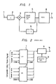
- FIG. 1 A prior art video memory apparatus for processing a video signal is shown in Fig. 1.
- a video signal is applied to an input terminal 1 and this video signal is then supplied to a multiplier 2 in which it is multiplied by a coefficient K (K ⁇ 1).
- the output signal from the multiplier 2 is supplied through an adder 3 to a frame delay circuit 4 in which it is delayed by a delay time of one frame period.
- the output signal from the frame delay circuit 4 is supplied to a multiplier 5 in which it is multiplied by a coefficient 1 - K.
- the output signal from the multiplier 5 is supplied to the adder 3 in which it is added with the output signal from the multiplier 2.
- the output signal from the frame delay circuit 4 is supplied through a first-in-first-out memory (hereinafter simply referred to as FIFO) circuit 6 to an output terminal 7.
- FIFO first-in-first-out memory
- the multiplier 2, the adder 3, the frame delay circuit 4 and the multiplier 5 constitute a kind of low pass filter having a time constant K and which constitutes a noise reducer circuit for reducing a noise component contained in the video signal.
- the frame delay circuit 4 may be formed of a generally available dynamic random access memory (hereinafter simply referred to as a DRAM). Since the frame delay circuit 4 operates at low speed, a serial-parallel converter and a parallel-serial converter are connected to the input and output sides of this frame delay circuit 4 though not shown.
- the FIFO circuit 6 is used as a time base corrector. According to this FIFO circuit 6, the data supplied thereto is written in its memory by a write clock synchronized with an incoming video signal and in which the written data is read out from the memory by a reference read clock asynchronous to the write clock and which is developed externally. Also, since this FIFO circuit 6 operates at low speed, a serial-parallel converter and a parallel-serial converter are connected to the input and output sides thereof though not shown.
- the known video memory When the known video memory is constructed as shown in Fig. 1, a plurality of memories are used to reduce the noise component and to correct the time base error thereby to improve the quality of a picture.
- the known video memory since the frame memory is used to reduce the noise component and the FIFO memory is used to correct the time base error, the known video memory is complicated in circuit arrangement. Further, these memories require control circuits for their operation. This makes the peripheral circuit complicated, the system large in size and causes several defects from a cost standpoint and from a design standpoint.
- a frequency converter circuit is used in the above mentioned video memory apparatus.
- This frequency converter is suitable for a video memory apparatus.
- the known frequency converter circuit (frame synchronizer) for converting a frequency is constructed, as for example, shown in Fig. 2.
- These frame memories 1 and 2 are supplied with data of the upper 4 bits and data of the lower 4 bits of a composite color video signal of 8 bits. That is, the frame memories 1 and 2 are each adapted to write data of 4 bits supplied thereto in turn in response to a write clock signal CKW and to read the same in response to a read clock signal CKR. At that time, the write clock signal CKW and the read clock signal CKR are not synchronized with each other so that the frame memories 1 and 2 generate output signals of frequencies different from those of the input signals, or output signals which are frequency-converted.
- a crossing detecting circuit 3 When “crossing” occurs between a write address signal and a read address signal used in the frame memories 1 and 2 as will be described later, this crossing is detected by a crossing detecting circuit 3. Then, on the basis of the detected results from the crossing detecting circuit 3, a chroma inverter 4, to which the data read out from the memories 1 and 2 are supplied, shifts the phase of a subcarrier by 180° and supplies a video signal with correct color reproduction to an output terminal 5.
- the frame memories 1 and 2 may be each constructed, for example as shown in Fig. 3.
- a video signal applied to an input terminal 10 is sequentially written in a serial access memory (hereinafter referred to as SAM) 11 of a line unit in response to the write clock CKW.
- SAM serial access memory
- the data written in the SAM 11 is transferred to a DRAM (dynamic random access memory) 12 and written in the DRAM 12 at its predetermined position designated by an address signal from a write address circuit 13 formed of a counter and which is supplied with a clock signal CLK.
- DRAM dynamic random access memory
- the data written in the predetermined position of the DRAM 12 is designated by an address signal from a read address circuit 14, which is formed of a counter and supplied with the clock signal CLK, read out therefrom and transferred to and written in a SAM 16.
- the data transferred to the SAM 16 is shifted bit by bit each time the read clock signal CKR is supplied to the SAM 16 and then supplied to an output terminal 17.
- the SAMs 11 and 16 are of the same storage capacity and the clock signals CKW and CKR are not synchronized with each other.
- the field information of an n-th field would be read out from t1 to t2; the field information of an (n + 1)-th field would be read out from the time t2 to t4; the field information of an (n + 2)-th field would be read out from t4 to t5; and the field information of an (n + 3)-th field would be read out from time t5 to t6.
- the field information of the (n + 1)-th field namely, the field information at the present field is read out from time t2 to t3 but the field information of the n-th field, or field information before the preceding field information is read out from time point t3 to t4 as shown in Fig. 4.
- the field information of one field before such as the field information of the (n + 1)-th field is read out out from the time t4 to t5 and the field information of the (n + 2)-th field is read out from time t5 to t6 and so on.
- the above mentioned crossing does not cause any trouble, if it occurs both in the frame memories 1 and 2 simultaneously. However, it causes a serious trouble if the crossing does not occur at the same time between the frame memories 1 and 2 due to the scattering of delay in the memories 1 and 2. That is, at that time the field information and the field information of one field before are mixed between the upper 4 bits and the lower 4 bits. As a result, this exerts a fatal bad influence upon the picture.
- the prior art video memory apparatus as described above comprises the features a, b, c, d, e, h, i, and j of claim 1 as enclosed. Also an address generating means is provided, however this means differs from the means g of claim 1 in that it does not provide a second read clock.
- the part of the prior art video memory apparatus which comprises the just mentioned features performs the noise reduction.
- a time base correction is provided by the "FIFO-memory 6".
- a video memory apparatus having the features a - h of claim 1, i. e. the features of the preamble of claim 1, is described in US-A-4,339,803.
- a write address signal and the two read address signals are all asynchronously with each other.
- the output terminal receives its signal from the signal processing means.
- a video apparatus for correcting time base errors and for compensation dropouts is described in EP-A-0 163 504.
- Said apparatus comprises the features a, b, c, e, f, g, h, i, and k of claim 1 as enclosed. It also comprises a memory means, similar to the frame memory means according to feature d of claim 1, however, this memory means has a storage capacity less than one frame.
- the apparatus further comprises a signal processing means for compensating dropouts. The signal from said signal processing means is only switched to the input buffer means in case that a dropout detector detects a dropout.
- This apparatus has very simple construction by combining the features as known from EP-A-0 163 504 into the apparatus as described in US-A-4,339,803. Further, the apparatus of the present invention is provided with means for handling the write address and the second read address when crossings occur due to the fact that these addresses are clocked asynchronously. Such means are similarly known from US-A-4,249,198, however, in the apparatus according to this US-patent, coincidence is not detected by comparing the address signals by using input and output signals, and addition or subtraction of a fixed value is not provided on the output side but on the input side of a memory means.
- a frame memory (or field memory) used in the video memory apparatus of this invention will be described first with reference to Fig. 5 which shows a main portion of this frame memory.
- a video signal is supplied to an input terminal 10 as serial data.
- the serial data applied to the input terminal 10 is supplied to and sequentially written in a SAM 11 unit which functions as an input buffer means in response to a write clock signal CKW.
- Data written in the SAM 11 is transferred to a DRAM 12 in parallel over a data bus, and then written in the DRAM 12 at a predetermined address designated by an address signal from a write address circuit 13.
- Data written in the DRAM 12 at a predetermined address is read out therefrom in parallel by the address signal from a first read address circuit 14, transferred to and written in a SAM 16 used as a first output buffer means.
- Information transferred to the SAM 16 is shifted by one bit each time the SAM 16 is supplied with a read clock signal CKR1 and then supplied to an output terminal 17 as a first output OUT1.
- Data written into the DRAM 12 at another predetermined address is read out therefrom in parallel by an address signal from a second read address circuit 14A, transferred to and written in a SAM 18 used as a second output buffer means.
- Information transferred to the SAM 18 is shifted by one bit each each time the SAM 18 is supplied with a read clock signal CKR2 and then supplied to an output terminal 19 as a second output OUT2.
- the SAMs 11, 16 and 18 are selected to have the same storage capacity.
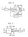
- Fig. 6 schematically illustrates an embodiment of a video memory apparatus according to the present invention which employs the frame memory as shown in Fig. 5. This embodiment can achieve the function of a time base corrector and the function of a noise reducer by using the same frame memory.
- like parts corresponding to those of Fig. 1 are marked with the same references and will not be described in detail.
- a frame memory 20 constructed as shown in Fig. 5.
- the input terminal 10 of the frame memory 20 is connected to the output side of the adder 3 and the output terminal 17 thereof is connected to the input side of the multiplier 5.
- the output terminal 19 of the frame memory 20 is connected to an output terminal 21.
- the read clock signal CKR1 applied to the SAM 16 within the frame memory 20 is synchronized with the write clock signal CKW applied to the SAM 11.
- the read clock signal CKR2 applied to the SAM 18 is made asynchronous to the read clock signal CKR1 and to the write clock signal CKW, and constitutes a reference signal which is developed externally.
- the read clock signal CKR1 and the write clock signal CKW are asynchronous to the read clock signal CKR2, it is necessary to prevent transfer pulses from respective ports from being transferred simultaneously during a period of one horizontal line (corresponding to the duration of 1H where H is one horizontal scanning period).
- the data applied to the input terminal 10 is written in the SAM 11 in response to the clock signal CKW and then transferred through the DRAM 12 to the SAM 16.
- the data transferred to the SAM 16 is read out therefrom in response to the read clock signal CKR1 synchronized with the clock signal CKW, the input data and the output data are delayed by a delay time of substantially one frame period. Then, the output data is supplied through the multiplier 5 to the adder 3 thereby to form a kind of cyclic-type filter, to achieve the noise reducer function.
- Fig. 7 schematically illustrates another embodiment of the video memory apparatus according to the present invention which employs the frame memory shown in Fig. 5. According to this embodiment, the same frame memory is used to achieve the function of the time base corrector and the function of a comb filter.
- the output terminals 17 and 19 of the frame memory 20 are connected to respective input terminals of an adder 22, and a 1/2 attenuator 23 is connected to receive the output of the adder 22.
- the write clock signal CKW applied to the SAM 11 and the read clock signals CKR1 and CKR2 applied to the SAMs 16 and 18 of the frame memory 20 (Fig. 5) are made asynchronous to one another and the read clock signals CKR1 and CKR2 are synchronized with each other, and are used as reference signals developed externally. Since the write clock signal CKW is made asynchronous to the read clock signals CKR1 and CKR2, also in this case, it is necessary to prevent transfer pulses of the respective ports from being overlapped simultaneously during a period of one horizontal line (1H).
- data is written in the SAM 11 in response to the clock signal CKW containing the jitter component and data are read out from the SAMs 16 and 18 in response to the fixed reference clock signals CKR1 and CKR2 containing no jitter component, whereby the function of the time base corrector can be achieved.
- the video signal consists of a luminance signal Y and a chrominance signal C and the chrominance signal C is inverted at every line so that if the video signal of the present line is taken as Y + C, a video signal of a next line is expressed as Y - C. Accordingly, when both of the video signals Y + C and Y - C are added and then the sum is divided by 2, can be established. Thus, the luminance signal Y can be separated from the video signal. Therefore, according to this embodiment, when the respective output signals from the SAMs 16 and 18 are added by the adder 22 and the added output therefrom is divided by 2 by the 1/2 attenuator 23, the separated luminance signal can be obtained at the output terminal 21. That is, the same function as that of the comb filter can be achieved.
- the input buffer means is connected to the input side of the memory means
- the first and second output buffer means are connected to the output side of the memory means and the input buffer means is made asynchronous to at least either the first or second output buffer means.
- Fig. 8 is a block diagram showing a circuit arrangement of this embodiment.
- the frame memory shown in Fig. 3 is employed so that in Fig. 8, like parts corresponding to those of Fig. 3 are marked with the same references and will not be described in detail.
- a comparator 30 which compares the address signal from the write address circuit 13 and the address signal from the read address signal circuit 14.
- the comparator 30 generates a flag signal when one address signal crosses the other.
- the flag signal from the comparator 30 is supplied to the input terminals D of a pair of flip-flop circuits 31 and 32.
- the clock signal CLK applied to the read address circuit 14 is supplied to the clock terminal of the flip-flop circuit 31 and also supplied through an inverter 33 to the clock terminal of the flip-flop circuit 32.
- the output of the flip-flop circuit 31 is supplied to a set terminal SET2 of a switching control circuit 34, while the output of the flip-flop circuit 32 is supplied to a set terminal SET1 of the switching control circuit 34.
- the switching control circuit 34 controls a switch 35 so as to connect its movable contact c to one fixed contact a during a vertical blanking period of the reading.
- the switching control circuit 34 controls the switch 35 so as to connect its movable contact c to the fixed contact a after a predetermined period of time, for example, 2H following the signal "1" being supplied thereto.
- the other fixed contact b of the switch 35 is connected through a 2H delay circuit 36 to the output side of the SAM 16 and the fixed contact a of the switch 35 is directly connected to the output side of the SAM 16.
- the common terminal c of the switch 35 is connected to an output terminal 37.
- the output signals from the flip-flop circuits 31 and 32 are supplied to an address correcting circuit 38, responsive to the output signals from the flip-flop circuits 31 and 32, the address correcting circuit 38 controls the write address circuit 13 or the read address circuit 14. Specifically, when the flip-flop circuit 32 generates an output "1" and the flip-flop circuit 31 generates an output "0", the address correcting circuit 38 controls the read address circuit 14 so as to make the sequential order of its address signal as -2, while when the flip-flop circuit 31 generates the output "1" and the flip-flop circuit 32 generates the output "0", the address correcting circuit 38 controls the write address circuit 13 so as to make the sequential order of its address signal by +2. In other words, the state of the applicable address circuit is increased or decreased by 2.
- Figs 9A to 9F are respectively diagrams used to explain flag signals generated at the output side of the comparator 30.
- a clock signal CLK shown in Fig. 9A is supplied to the read address circuit 14 and to the clock terminal of the flip-flop circuit 31. This clock signal CLK is further supplied through the inverter 33 to the clock terminal of the flip-flop circuit 32.
- the state of the read address signal, shown in Fig. 9B, from the read address circuit 14 is higher than that of the write address signal, shown in Fig. 9C, from the write address circuit 13, as will be clear from Figs. 9B and 9C, the read address signal crosses the write address signal.
- the comparator 30 When the read address signal coincides with the write address signal in part, or the read address signal crosses the write address signal, the comparator 30 generates a flag signal shown in Fig. 9D. For example, when (n - 1)-th, n-th and (n + 1)-th read and write address signals coincide with one another in part, the comparator 30 generates flag signals as shown in Figs. 9B to 9D.
- the write address signal crosses the read address signal.
- the comparator 30 When the write address signal coincides with the read address signal in part, or the write address signal crosses the read address signal, the comparator 30 generates a flag signal shown in Fig. 9F.
- the comparator 30 generates the flag signals when the (n - 2)-th, (n - 1)-th and n-th read and write address signals coincide with one another in part as shown in Figs. 9B, 9E and 9F.
- the flag signal generated at the output side of the comparator 30 is supplied to the D input terminals of the flip-flop circuits 31 and 32, so that when the clock signal CLK applied to the read address circuit 14 is supplied to the clock terminals of the flip-flop circuits 31 and 32, the flag signal is manifested by the flip-flop circuits 31 and 32 at their output terminals Q.
- the read address signal (Fig. 9B) crosses the write address signal (Fig. 9C) the flag signal shown in Fig. 9D is generated, and the flip-flop circuit 32, at the time of the trailing edge of the clock signal CLK shown in Fig. 9A. generates the output "1" (while the flip-flop circuit 31 generates the output "0"); and when the write address signal (Fig.
- the switch control circuit 34 Upon normal operation, in which the read and write address signals do not cross with each other, the switch control circuit 34 allows the movable contact c of the switch 35 to be connected to its fixed contact b , so that the frame memory, or the SAM 16 generates the video signals corresponding to the (n - 2)-th, (n - 1)-th, n-th, (n + 1)-th, ..., (n + 5)-th address signals, in turn as shown in Fig. 10A.
- the flip-flop circuit 32 when the read address signal crosses the write address signal as described above, the flip-flop circuit 32 generates the output "1" and the flip-flop circuit 31 generates the output "0", with the result that the address correcting circuit 38 controls the read address circuit 14 so as to shift the timing at which the crossing occurs, for example, n-th address by - 2 as shown in Fig. 10A.
- the (n - 2)-th address signal is generated from the read address circuit 14 and supplied to the DRAM 12.
- the read address circuit 14 sequentially generates the address signals in the shifted form, such as (n - 1)-th address signal for (n + 1)-th address signal, (n + 3)-th address signal for (n + 1)-th address signal, ..., by -2 each.
- the switching control circuit 34 controls the switch 35 so as to allow its movable contact c to be connected to the contact a .
- the address correcting circuit 38 controls the write address circuit 13 so as to shift an address signal at a crossing time point, for example, an n-th address signal by +2 as shown in Fig. 11A and to supply and (n +2)-th address signal to the DRAM 12. Then, a video signal corresponding to the n-th address signal is written in the DRAM 12 at its predetermined position corresponding to the (n + 2)-th address signal.
- video signals V1, V2, V3, ..., V n are written in and read out in turn in response to the respective addresses 1, 2, 3, ...
- the switch control circuit 34 supplies the control signal to the switch 35, so that the switch 35 connects its movable contact c to the fixed contact a .
- video signals V n - 4 , V n - 3 , V n - 2 and V n - 1 corresponding to the (n - 4)-th, (n - 3)-th, (n - 2)-th and (n - 1)-th address signals (Fig.
- the frequency converting circuit of the present invention when it is found that the crossing occurs between the first and second address signals as the result of the comparison of them, the sequential order in which the address signal is supplied to the memory is switched and the continuous output signal is derived from the memory, so that the occurrence of the crossing between the address signals can be avoided. Accordingly, when input data is processed in the data form of upper and lower bits, no trouble occurs and it becomes possible to prevent a serious bad influence from being exerted upon the picture which was a disadvantage of the prior art.
- the crossing itself between the address signals can be avoided, so that unlike the prior art, the crossing detection circuit, the chroma inverter or the like can be removed, with the circuit arrangement being simplified accordingly.
Landscapes
- Engineering & Computer Science (AREA)
- Multimedia (AREA)
- Signal Processing (AREA)
- Picture Signal Circuits (AREA)
- Television Signal Processing For Recording (AREA)
Claims (2)
- Videospeichervorrichtung zum Erzielen von Störsignalverringerung und Zeitbasiskorrektur, welche Vorrichtung folgendes aufweist:a) einen Eingangsanschluß (1) zum Eingeben von Videosignalen;b) eine Signalverarbeitungseinrichtung (2, 3, 5) zum Verarbeiten sowohl der eingegebenen Videosignale als auch von Videosignalen, die aus einer Vollbildspeichereinrichtung (12) durch eine erste Ausgangspuffereinrichtung (16) und eine zweite Ausgangspuffereinrichtung (18) ausgelesen werden;c) eine Eingangspuffereinrichtung (11) zum Empfangen der von der Signalverarbeitungseinrichtung ausgegebenen Signale, und zum Zuführen ihrer Ausgangssignale an die Vollbildspeichereinrichtung in Übereinstimmung mit einem Schreibtakt (CKW);d) die genannte Vollbildspeichereinrichtung (12);e) die genannte erste Ausgangspuffereinrichtung (16), die Signale von der Vollbildspeichereinrichtung mit einem ersten Lesetakt (CKR1) liest;f) die genannte zweite Ausgangspuffereinrichtung (18), die Signale von der Vollbildspeichereinrichtung mit einem zweiten Lesetakt (CKR2) liest;g) eine Adreßerzeugungseinrichtung (13, 14, 14A) zum Adressieren der Vollbildspeichereinrichtung abhängig vom Schreibtakt und dem ersten und dem zweiten Lesetakt; undh) einen Ausgangsanschluß (19), der die Ausgangssignale der zweiten Ausgangspuffereinrichtung erhält;
dadurch gekennzeichnet, daßi) die Eingangspuffereinrichtung und die erste Ausgangspuffereinrichtung synchron getaktet werden, wodurch die erste Ausgangspuffereinrichtung Signale empfängt, die gegenüber den Eingangssignalen im wesentlichen um ein Vollbild verschoben sind;j) die Signalverarbeitungseinrichtung (2, 3, 5) so ausgebildet ist, daß sie zum Erzielen von Störsignalverringerung- die Eingangssignale mit einem Faktor K multipliziert;- die von der ersten Ausgangspuffereinrichtung ausgegebenen Signale mit einem Faktor 1 - K multipliziert;- die zwei Multiplikationsergebnisse addiert; und- das Additionssignal an die Eingangspuffereinrichtung ausgibt;k) die zweite Ausgangspuffereinrichtung zum Erzielen einer Zeitbasiskorrektur mit einem zweiten Lesetakt getaktet wird, der asynchron zum Schreibtakt und zum ersten Lesetakt ist;l) eine Vergleichseinrichtung (30) vorhanden ist, um das Schreibadreßsignal und das zweite, asynchrone Leseadreßsignal miteinander zu vergleichen und ein Übereinstimmungssignal auszugeben;m) eine Adreßkorrekturschaltung (38) vorhanden ist, um die zweite Leseadresse um einen festgelegten Wert zu erhöhen, sobald das Übereinstimmungssignal anzeigt, daß die Schreibadresse die zweite Leseadresse überholt, und zum Erniedrigen der zweiten Leseadresse um den festgelegten Wert, sobald das Übereinstimmungssignal anzeigt, daß die zweite Leseadresse die Schreibadresse überholt;n) eine Verzögerungsschaltung (36) vorhanden ist, um das unter der zweiten Leseadresse ausgelesene Signal um eine Verzögerungszeitperiode zu verzögern, die einem ganzzahligen Vielfachen der horizontalen Synchronisierperiode entspricht, wobei die ganze Zahl ein festgelegter Wert ist; undo) eine Umschalteinrichtung (31, 32, 34, 35) vorhanden ist, um das verzögerte Signal auf den Ausgangsanschluß zu schalten, wenn das Übereinstimmungssignal geliefert wird, und um das unverzögerte Signal um eine vorgegebene Zeitspanne später an den Ausgangsanschluß zu liefern, wodurch das Umschalten auf das verzögerte Signal erfolgt, nachdem die Verzögerungszeitperiode ab Auftreten des Übereinstimmungssignals abgelaufen ist. - Vorrichtung nach Anspruch 1, dadurch gekennzeichnet, daß der festgelegte Wert "2" ist.
Applications Claiming Priority (4)
| Application Number | Priority Date | Filing Date | Title |
|---|---|---|---|
| JP61144075A JPH0734586B2 (ja) | 1986-06-20 | 1986-06-20 | 映像記憶装置 |
| JP144075/86 | 1986-06-20 | ||
| JP150493/86 | 1986-06-26 | ||
| JP61150493A JPH07114504B2 (ja) | 1986-06-26 | 1986-06-26 | 周波数変換回路及び周波数変換方法 |
Publications (3)
| Publication Number | Publication Date |
|---|---|
| EP0249985A2 EP0249985A2 (de) | 1987-12-23 |
| EP0249985A3 EP0249985A3 (en) | 1989-08-23 |
| EP0249985B1 true EP0249985B1 (de) | 1993-09-08 |
Family
ID=26475607
Family Applications (1)
| Application Number | Title | Priority Date | Filing Date |
|---|---|---|---|
| EP87108801A Expired - Lifetime EP0249985B1 (de) | 1986-06-20 | 1987-06-19 | Videospeicher |
Country Status (3)
| Country | Link |
|---|---|
| US (1) | US4864402A (de) |
| EP (1) | EP0249985B1 (de) |
| DE (1) | DE3787324T2 (de) |
Families Citing this family (25)
| Publication number | Priority date | Publication date | Assignee | Title |
|---|---|---|---|---|
| EP0309875A3 (de) * | 1987-09-30 | 1991-02-06 | Deutsche Thomson-Brandt GmbH | Demultiplexer |
| DE3804175A1 (de) * | 1988-02-11 | 1989-08-24 | Broadcast Television Syst | Verfahren und schaltungsanordnung zum einschreiben und auslesen eines digitalen halbleiterspeichers fuer videosignale |
| US5325187A (en) * | 1988-04-27 | 1994-06-28 | Canon Kabushiki Kaisha | Image processing apparatus with back porch period sampling and clamping |
| US6408127B1 (en) | 1988-04-27 | 2002-06-18 | Canon Kabushiki Kaisha | Image processing apparatus |
| US5387945A (en) * | 1988-07-13 | 1995-02-07 | Seiko Epson Corporation | Video multiplexing system for superimposition of scalable video streams upon a background video data stream |
| JP2748562B2 (ja) | 1988-07-13 | 1998-05-06 | セイコーエプソン株式会社 | 画像処理装置 |
| JP2796329B2 (ja) * | 1989-02-08 | 1998-09-10 | 株式会社日立製作所 | 表示メモリとそれを備えた画像処理装置 |
| FR2653629B1 (fr) * | 1989-10-20 | 1995-07-07 | Europ Rech Electr Lab | Dispositif de compensation de mouvement et recepteur de television comportant un tel dispositif. |
| US5157775A (en) * | 1989-12-15 | 1992-10-20 | Eastman Kodak Company | Dual port, dual speed image memory access arrangement |
| JP2524857B2 (ja) * | 1990-04-09 | 1996-08-14 | ティアツク株式会社 | 画像再生装置 |
| JP2699614B2 (ja) * | 1990-06-06 | 1998-01-19 | 松下電器産業株式会社 | 画像メモリ装置 |
| FR2664779B1 (fr) * | 1990-07-13 | 1993-06-11 | Europ Rech Electr Lab | Procede de traitement d'un signal video. |
| KR920009770B1 (ko) * | 1990-10-31 | 1992-10-22 | 삼성전자 주식회사 | 영상기록재생장치에서 메모리내 프레임 데이타 어드레싱 방식 |
| US5315388A (en) * | 1991-11-19 | 1994-05-24 | General Instrument Corporation | Multiple serial access memory for use in feedback systems such as motion compensated television |
| EP0562221B1 (de) * | 1992-03-27 | 1997-10-15 | Alcatel | Videodekoder |
| JP3336630B2 (ja) * | 1992-06-23 | 2002-10-21 | ソニー株式会社 | 映像信号処理回路 |
| US5615355A (en) * | 1992-10-22 | 1997-03-25 | Ampex Corporation | Method and apparatus for buffering a user application from the timing requirements of a DRAM |
| JP2956527B2 (ja) * | 1995-04-28 | 1999-10-04 | 松下電器産業株式会社 | 画像メモリ機能付き映像装置 |
| US6806916B1 (en) | 1995-04-28 | 2004-10-19 | Matsushita Electric Industrial Co., Ltd. | Video apparatus with image memory function |
| JP3359270B2 (ja) * | 1997-10-24 | 2002-12-24 | キヤノン株式会社 | メモリー制御装置と液晶表示装置 |
| US6168249B1 (en) * | 1999-04-20 | 2001-01-02 | Chuan-Fu Chien | Computer mainframe housing for computer |
| JP2000358193A (ja) * | 1999-06-15 | 2000-12-26 | Matsushita Electric Ind Co Ltd | 画像メモリ機能付き映像装置 |
| FI118830B (fi) * | 2001-02-08 | 2008-03-31 | Nokia Corp | Tietovirran toisto |
| DE10200990A1 (de) * | 2002-01-14 | 2003-08-14 | Broadcasttelevision Systems Me | Verfahren zur Speicherung von Videosignalen |
| GB2384409B (en) * | 2002-01-16 | 2005-05-11 | Thomson Licensing Sa | Method and arrangement for correcting data |
Family Cites Families (10)
| Publication number | Priority date | Publication date | Assignee | Title |
|---|---|---|---|---|
| US4101926A (en) * | 1976-03-19 | 1978-07-18 | Rca Corporation | Television synchronizing apparatus |
| US4339803A (en) * | 1976-10-14 | 1982-07-13 | Micro Consultants Limited | Video frame store and real time processing system |
| US4240106A (en) * | 1976-10-14 | 1980-12-16 | Micro Consultants, Limited | Video noise reduction |
| JPS6043707B2 (ja) * | 1978-03-08 | 1985-09-30 | 株式会社東京放送 | 位相変換装置 |
| JPS5984314A (ja) * | 1982-11-05 | 1984-05-16 | Victor Co Of Japan Ltd | 情報記録円盤再生装置 |
| JPS60177786A (ja) * | 1984-02-24 | 1985-09-11 | Hitachi Denshi Ltd | 映像信号処理装置 |
| JP2544323B2 (ja) * | 1984-05-26 | 1996-10-16 | ソニー株式会社 | 再生映像信号補正回路 |
| US4646151A (en) * | 1985-02-01 | 1987-02-24 | General Electric Company | Television frame synchronizer with independently controllable input/output rates |
| US4746980A (en) * | 1985-02-04 | 1988-05-24 | Petersen Alfred C | Video processing system |
| US4677470A (en) * | 1986-04-22 | 1987-06-30 | Fuji Photo Optical Company, Ltd. | Image reversal correction system for video endoscopes |
-
1987
- 1987-06-19 EP EP87108801A patent/EP0249985B1/de not_active Expired - Lifetime
- 1987-06-19 DE DE87108801T patent/DE3787324T2/de not_active Expired - Lifetime
- 1987-06-19 US US07/064,013 patent/US4864402A/en not_active Expired - Lifetime
Also Published As
| Publication number | Publication date |
|---|---|
| DE3787324T2 (de) | 1994-03-31 |
| EP0249985A2 (de) | 1987-12-23 |
| US4864402A (en) | 1989-09-05 |
| EP0249985A3 (en) | 1989-08-23 |
| DE3787324D1 (de) | 1993-10-14 |
Similar Documents
| Publication | Publication Date | Title |
|---|---|---|
| EP0249985B1 (de) | Videospeicher | |
| US4712130A (en) | Chrominance signal frequency converter as for a pix-in-pix television receiver | |
| CA1240788A (en) | Compression of pixels in a reduced-size video image | |
| US5331346A (en) | Approximating sample rate conversion system | |
| US5532749A (en) | Sample rate conversion device for processing non-standard television signal | |
| EP0196826A1 (de) | Filtersystem zur Verarbeitung eines Fernsehbildes mit verminderter Auflösung | |
| CA1260605A (en) | Standard converting apparatus | |
| US3949416A (en) | Drop out compensation system | |
| JPH0191576A (ja) | 時間伸長されたビデオ信号発生回路 | |
| US4656516A (en) | Vertical subsampling and memory synchronization system for a picture within a picture television receiver | |
| EP0122561B1 (de) | Synchronisiereinrichtung für ein Fernsehvideosignal | |
| JPH0370374A (ja) | 表示システム | |
| US6404458B1 (en) | Apparatus for converting screen aspect ratio | |
| JPH0155632B2 (de) | ||
| US5493589A (en) | Circuit arrangement for synchronizing a data stream | |
| US4716454A (en) | Chroma phase word encode/decode in a video processing system | |
| US5495293A (en) | Frame synchronizer and a signal switching apparatus | |
| US5537154A (en) | Edge compensation method and apparatus of image signal | |
| JPS637593A (ja) | 周波数変換回路及び周波数変換方法 | |
| Kano et al. | Television frame synchronizer | |
| GB2072457A (en) | Method and apparatus for one line dropout compensation of color television signals | |
| KR100202542B1 (ko) | 영상신호처리기의 휘도/색신호 분리회로 | |
| JP3038725B2 (ja) | タイムベースコレクタ | |
| JP2522193B2 (ja) | 水平同期信号変換装置 | |
| JPH011378A (ja) | 縮小画面用映像信号処理回路 |
Legal Events
| Date | Code | Title | Description |
|---|---|---|---|
| PUAI | Public reference made under article 153(3) epc to a published international application that has entered the european phase |
Free format text: ORIGINAL CODE: 0009012 |
|
| AK | Designated contracting states |
Kind code of ref document: A2 Designated state(s): DE FR GB NL |
|
| PUAL | Search report despatched |
Free format text: ORIGINAL CODE: 0009013 |
|
| AK | Designated contracting states |
Kind code of ref document: A3 Designated state(s): DE FR GB NL |
|
| 17P | Request for examination filed |
Effective date: 19900222 |
|
| 17Q | First examination report despatched |
Effective date: 19911223 |
|
| GRAA | (expected) grant |
Free format text: ORIGINAL CODE: 0009210 |
|
| AK | Designated contracting states |
Kind code of ref document: B1 Designated state(s): DE FR GB NL |
|
| REF | Corresponds to: |
Ref document number: 3787324 Country of ref document: DE Date of ref document: 19931014 |
|
| ET | Fr: translation filed | ||
| PLBE | No opposition filed within time limit |
Free format text: ORIGINAL CODE: 0009261 |
|
| STAA | Information on the status of an ep patent application or granted ep patent |
Free format text: STATUS: NO OPPOSITION FILED WITHIN TIME LIMIT |
|
| 26N | No opposition filed | ||
| REG | Reference to a national code |
Ref country code: GB Ref legal event code: IF02 |
|
| PGFP | Annual fee paid to national office [announced via postgrant information from national office to epo] |
Ref country code: NL Payment date: 20060604 Year of fee payment: 20 |
|
| PGFP | Annual fee paid to national office [announced via postgrant information from national office to epo] |
Ref country code: FR Payment date: 20060608 Year of fee payment: 20 |
|
| PGFP | Annual fee paid to national office [announced via postgrant information from national office to epo] |
Ref country code: GB Payment date: 20060614 Year of fee payment: 20 |
|
| PGFP | Annual fee paid to national office [announced via postgrant information from national office to epo] |
Ref country code: DE Payment date: 20060615 Year of fee payment: 20 |
|
| PG25 | Lapsed in a contracting state [announced via postgrant information from national office to epo] |
Ref country code: NL Free format text: LAPSE BECAUSE OF EXPIRATION OF PROTECTION Effective date: 20070619 |
|
| REG | Reference to a national code |
Ref country code: GB Ref legal event code: PE20 |
|
| NLV7 | Nl: ceased due to reaching the maximum lifetime of a patent |
Effective date: 20070619 |
|
| PG25 | Lapsed in a contracting state [announced via postgrant information from national office to epo] |
Ref country code: GB Free format text: LAPSE BECAUSE OF EXPIRATION OF PROTECTION Effective date: 20070618 |