EP0247569B1 - Circuit de récupération d'horloge - Google Patents
Circuit de récupération d'horloge Download PDFInfo
- Publication number
- EP0247569B1 EP0247569B1 EP87107614A EP87107614A EP0247569B1 EP 0247569 B1 EP0247569 B1 EP 0247569B1 EP 87107614 A EP87107614 A EP 87107614A EP 87107614 A EP87107614 A EP 87107614A EP 0247569 B1 EP0247569 B1 EP 0247569B1
- Authority
- EP
- European Patent Office
- Prior art keywords
- regeneration
- clock
- regeneration circuits
- clock pulse
- pulses
- Prior art date
- Legal status (The legal status is an assumption and is not a legal conclusion. Google has not performed a legal analysis and makes no representation as to the accuracy of the status listed.)
- Expired - Lifetime
Links
- 238000011084 recovery Methods 0.000 title 1
- 230000008929 regeneration Effects 0.000 claims abstract description 37
- 238000011069 regeneration method Methods 0.000 claims abstract description 37
- 238000010897 surface acoustic wave method Methods 0.000 claims abstract description 14
- 230000003247 decreasing effect Effects 0.000 claims abstract description 4
- 238000000605 extraction Methods 0.000 claims description 12
- 230000002123 temporal effect Effects 0.000 description 5
- 238000010586 diagram Methods 0.000 description 4
- 230000005540 biological transmission Effects 0.000 description 3
- 238000005516 engineering process Methods 0.000 description 2
- 230000010355 oscillation Effects 0.000 description 2
- 238000004519 manufacturing process Methods 0.000 description 1
- 239000013307 optical fiber Substances 0.000 description 1
- 230000001172 regenerating effect Effects 0.000 description 1
- 230000001360 synchronised effect Effects 0.000 description 1
Images
Classifications
-
- H—ELECTRICITY
- H04—ELECTRIC COMMUNICATION TECHNIQUE
- H04L—TRANSMISSION OF DIGITAL INFORMATION, e.g. TELEGRAPHIC COMMUNICATION
- H04L7/00—Arrangements for synchronising receiver with transmitter
- H04L7/02—Speed or phase control by the received code signals, the signals containing no special synchronisation information
- H04L7/027—Speed or phase control by the received code signals, the signals containing no special synchronisation information extracting the synchronising or clock signal from the received signal spectrum, e.g. by using a resonant or bandpass circuit
Definitions
- the invention relates to a plurality of regeneration circuits consisting of at least two clock regeneration circuits, which are each provided for different clock frequencies and each contain at least one SAW (surface acoustic wave) filter module, to which an input-side clock extraction circuit supplies pulses obtained from data pulses.
- SAW surface acoustic wave
- Clock regeneration circuits have long been realized with the aid of a bandpass filter which is fed by pulses which are derived from the received data pulses.
- a clock regeneration circuit is known from US Pat. No. 4,004,162, in which, with the aid of a clock extraction circuit which essentially consists of a differentiating element and a rectifier arrangement connected downstream of the differentiating element, the data pulses received by the regenerating circuit are processed and then fed to a bandpass filter.
- the bandpass has a center frequency that is tuned to the clock frequency of the data pulses.
- the band-pass filter is excited to oscillations which have the frequency of the signal clock by the output pulses of the clock extraction circuit.
- a clock signal can be obtained from these oscillations, with the aid of which the incoming data pulses which have been ground in the pulse shape can be regenerated in the correct phase.
- the bandpass filter in such a clock regeneration circuit has recently been frequently implemented by a SAW filter which operates using surface acoustic waves, cf. IEEE, Journal on Selected Areas in Communications, Vol. SAC-2, No. 6, November 1984, pages 957-965.
- this object is achieved in that at least the clock extraction circuit of each regeneration circuit is an IC module that is the same for all regeneration circuits, the output pulses of which have the same pulse length for all regeneration circuits, and that the filter modules for this plurality of regeneration circuits each have a function of that have selected clock frequency and increasing with decreasing clock frequency phase.
- a load resistor provided on the output side of the filter module is at least partially designed as an adjustable resistor and / or that the adjustable load resistor is at least partially configured as a thermistor.
- the IC module is designed so that it can be switched over in such a way that the length of the output pulses of the clock extraction circuit can be changed in steps.
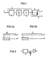
- the clock regeneration circuit essentially consists of three circuit components, namely a clock extraction circuit 1, to which relatively smoothed data pulses are supplied via an incoming data line 2.
- the data pulses are distributed as a random sequence over the temporal locations, which are determined by a signal clock which, as the so-called bit frequency, determines the maximum temporal sequence of the data pulses.
- the clock extraction circuit 1 essentially contains a differentiating element and a rectifier circuit, is connected on the output side to a SAW filter module 3 and supplies it with pulses 4 (compare also FIGS. 2a and 2b) of a relatively short duration, the length of time of these pulses being independent of the bit frequency of the data transmission, i.e. the clock frequency, is always the same.
- the filter module 3 is excited by the output pulses of the module 1 to vibrations that correspond to the clock frequency, so that the clock frequency is available at the output of the filter module 3.
- the vibrations of the filter module 3 are processed so that 5 clock frequency pulses are available at the output of the module, which are suitable for controlling a flip-flop 6.
- the flip-flop 6 also receives the data pulses arriving on line 2 via a line 7, so that the flip-flop 6 is connected to an output 8 Regenerated data pulses can be taken, which are synchronized in phase with the respective time location of a clock pulse.
- the signal clock can also be taken from the module 5 via a line 9.
- Modules 1, 5 and 6 are particularly suitable for this.
- a e.g. The blocks 1, 5 and 6 realizing IC circuit, which is also to be used in regeneration circuits for different clock frequencies, has the disadvantage, however, that as shown in FIGS Data regeneration in module 6 required clock pulses 4 to drive module 6 in the correct phase (FIG. 2a), so that data regeneration in module 6 is effective.
- the temporal position of a regenerated clock pulse 4 compared to a now longer data pulse 11 is unfavorable for an effective regeneration of the data pulse in the module 6 (FIG. 2b).
- the SAW filter module 3 is therefore provided with a phase which is greater, the lower the clock frequency for which the filter module 3 is intended. This is possible, for example, very simply by differently dimensioning the distance between the transmitter electrode configuration and the receiver electrode configuration of the SAW filter module.
- the SAW module 3 which anyway has to be tailored to the respective clock frequency for regeneration circuits which are provided for different clock frequencies, is provided with an increasing phase with decreasing clock frequency.
- a clock pulse 4 which drives the module 6 is thereby always effective at the module 6 in relation to a data pulse 11 in such a way that effective, in-phase data regeneration can be achieved with a circuit arrangement as shown in FIG. 1.
- a controllable load resistor 12 is provided at the output of the filter module 3 (FIG. 3). If a thermistor is used for at least part of the load resistor 3, an undesired change in the phase of the module 3, which is caused by temperature fluctuations, can thereby be compensated for.
Landscapes
- Engineering & Computer Science (AREA)
- Computer Networks & Wireless Communication (AREA)
- Signal Processing (AREA)
- Synchronisation In Digital Transmission Systems (AREA)
- Networks Using Active Elements (AREA)
- Surface Acoustic Wave Elements And Circuit Networks Thereof (AREA)
- Stereo-Broadcasting Methods (AREA)
- Stabilization Of Oscillater, Synchronisation, Frequency Synthesizers (AREA)
- Oscillators With Electromechanical Resonators (AREA)
- Electronic Switches (AREA)
Claims (4)
Priority Applications (1)
| Application Number | Priority Date | Filing Date | Title |
|---|---|---|---|
| AT87107614T ATE59919T1 (de) | 1986-05-28 | 1987-05-25 | Taktregenerierschaltung. |
Applications Claiming Priority (2)
| Application Number | Priority Date | Filing Date | Title |
|---|---|---|---|
| DE3617909 | 1986-05-28 | ||
| DE3617909 | 1986-05-28 |
Publications (2)
| Publication Number | Publication Date |
|---|---|
| EP0247569A1 EP0247569A1 (fr) | 1987-12-02 |
| EP0247569B1 true EP0247569B1 (fr) | 1991-01-09 |
Family
ID=6301779
Family Applications (1)
| Application Number | Title | Priority Date | Filing Date |
|---|---|---|---|
| EP87107614A Expired - Lifetime EP0247569B1 (fr) | 1986-05-28 | 1987-05-25 | Circuit de récupération d'horloge |
Country Status (7)
| Country | Link |
|---|---|
| US (1) | US4801818A (fr) |
| EP (1) | EP0247569B1 (fr) |
| JP (1) | JPH0831852B2 (fr) |
| AT (1) | ATE59919T1 (fr) |
| DE (1) | DE3767214D1 (fr) |
| ES (1) | ES2019331B3 (fr) |
| GR (1) | GR3001384T3 (fr) |
Families Citing this family (7)
| Publication number | Priority date | Publication date | Assignee | Title |
|---|---|---|---|---|
| JP2648928B2 (ja) * | 1988-04-28 | 1997-09-03 | 富士重工業株式会社 | 自動車用エンジンの気筒判別装置および気筒別制御方法 |
| TW242204B (fr) * | 1991-12-09 | 1995-03-01 | Philips Nv | |
| JPH08307401A (ja) * | 1995-05-10 | 1996-11-22 | Nec Corp | タイミング抽出回路 |
| US5870592A (en) * | 1996-10-31 | 1999-02-09 | International Business Machines Corp. | Clock generation apparatus and method for CMOS microprocessors using a differential saw oscillator |
| US6014047A (en) * | 1998-01-07 | 2000-01-11 | International Business Machines Corporation | Method and apparatus for phase rotation in a phase locked loop |
| US5949262A (en) * | 1998-01-07 | 1999-09-07 | International Business Machines Corporation | Method and apparatus for coupled phase locked loops |
| JP2000031889A (ja) * | 1998-07-13 | 2000-01-28 | Hitachi Ltd | スペクトラム拡散通信方式の移動通信端末 |
Family Cites Families (8)
| Publication number | Priority date | Publication date | Assignee | Title |
|---|---|---|---|---|
| FR1603165A (fr) * | 1968-07-22 | 1971-03-22 | ||
| US3760111A (en) * | 1970-06-20 | 1973-09-18 | Nippon Electric Co | Pulse regenerative repeater for a multilevel pulse communication system |
| GB1508780A (en) * | 1974-12-18 | 1978-04-26 | Plessey Co Ltd | Circuit for generating synchronisation signals |
| JPS5926136B2 (ja) * | 1975-01-25 | 1984-06-25 | 日本電気株式会社 | クロツク再生回路 |
| US3969590A (en) * | 1975-04-04 | 1976-07-13 | Rockwell International Corporation | Surface acoustic wave apparatus |
| US3985970A (en) * | 1975-04-11 | 1976-10-12 | Societe Lignes Telegraphiques Et Telephoniques | Regeneration of signalling pulses |
| DE2951022A1 (de) * | 1979-12-19 | 1981-07-23 | Robert Bosch Gmbh, 7000 Stuttgart | Schaltungsanordnung zur erzeugung von taktimpulsen bei der regenerierung von rechteckimpulsen |
| GB2128834B (en) * | 1982-10-16 | 1986-01-22 | Ferranti Plc | Circuit that produces long fm pulses |
-
1987
- 1987-05-01 US US07/044,772 patent/US4801818A/en not_active Expired - Fee Related
- 1987-05-25 DE DE8787107614T patent/DE3767214D1/de not_active Expired - Lifetime
- 1987-05-25 EP EP87107614A patent/EP0247569B1/fr not_active Expired - Lifetime
- 1987-05-25 AT AT87107614T patent/ATE59919T1/de not_active IP Right Cessation
- 1987-05-25 ES ES87107614T patent/ES2019331B3/es not_active Expired - Lifetime
- 1987-05-28 JP JP62130056A patent/JPH0831852B2/ja not_active Expired - Lifetime
-
1991
- 1991-01-28 GR GR90400382T patent/GR3001384T3/el unknown
Also Published As
| Publication number | Publication date |
|---|---|
| ATE59919T1 (de) | 1991-01-15 |
| JPH0831852B2 (ja) | 1996-03-27 |
| US4801818A (en) | 1989-01-31 |
| GR3001384T3 (en) | 1992-09-11 |
| JPS62290227A (ja) | 1987-12-17 |
| ES2019331B3 (es) | 1991-06-16 |
| EP0247569A1 (fr) | 1987-12-02 |
| DE3767214D1 (de) | 1991-02-14 |
Similar Documents
| Publication | Publication Date | Title |
|---|---|---|
| DE69506138T2 (de) | Akustisches Oberflächenwellenfilter | |
| DE10102153B4 (de) | Oberflächenwellenbauelement, sowie dessen Verwendung und Verfahren zu dessen Herstellung | |
| EP1248365A2 (fr) | Système à ondes de surface présentant au moins deux structures à ondes de surface | |
| DE2104779A1 (de) | Bandfilter-Schaltung | |
| EP0247569B1 (fr) | Circuit de récupération d'horloge | |
| DE102005061601A1 (de) | Resonatorfilter | |
| DE69506137T2 (de) | Akustisches Oberflächenwellenfilter | |
| DE2531151C3 (de) | Mit elastischen Oberflächenwellen arbeitende elektromechanische Einrichtung | |
| DE69330309T2 (de) | Akustisches oberflächenwellenfilter mit mehrfach-bandbreite | |
| DE102017108105B4 (de) | Filtervorrichtung für elastische Wellen | |
| DE69105527T2 (de) | Saw-laufzeitleitungen mit anzapfungen. | |
| DE69716846T2 (de) | Oberflächenwellen-Resonatorfilter | |
| DE1962220B2 (de) | Elektrostriktiv angetriebene Stimmgabel | |
| EP0487783B1 (fr) | Résonateur à ondes de surface | |
| DE10358347A1 (de) | Oberflächenwellenfilter | |
| DE1814954C3 (de) | Elektrische Filterweiche, bestehend aus zwei elektromechanischen Filtern mit unterschiedlicher Bandbreite | |
| DE102017208205A1 (de) | Filterelement mit veränderbarem Filterbereich, Verfahren zum Herstellen eines Filterelements und Verfahren zum Betreiben eines Filterelements | |
| DE1148591B (de) | Taktfrequenz-Generatoranordnung fuer Impulskodemodulations-Systeme | |
| DE2532227A1 (de) | Elektromechanische resonanzeinrichtung und ihre verwendung zur filterung von fernsehsignalen | |
| DE4227833C2 (de) | Zwischenfrequenzfilter für einen Funkempfänger | |
| DE2915507C2 (de) | Akustikwellen-Höchstfrequenzoszillator | |
| DE2738032C2 (de) | Elektromechanisches Filter | |
| DE102021212216A1 (de) | Hochfrequenz-Filtervorrichtung, Hochfrequenzmodul und Hochfrequenz-Filterverfahren | |
| DE2754026A1 (de) | Filtervorrichtung zur feststellung mehrerer frequenzen in einem elektrischen signal | |
| EP0004341A1 (fr) | Synchronisation d'un oscillateur local avec un oscillateur de référence |
Legal Events
| Date | Code | Title | Description |
|---|---|---|---|
| PUAI | Public reference made under article 153(3) epc to a published international application that has entered the european phase |
Free format text: ORIGINAL CODE: 0009012 |
|
| AK | Designated contracting states |
Kind code of ref document: A1 Designated state(s): AT BE CH DE ES FR GB GR IT LI LU NL SE |
|
| 17P | Request for examination filed |
Effective date: 19871218 |
|
| 17Q | First examination report despatched |
Effective date: 19900327 |
|
| GRAA | (expected) grant |
Free format text: ORIGINAL CODE: 0009210 |
|
| AK | Designated contracting states |
Kind code of ref document: B1 Designated state(s): AT BE CH DE ES FR GB GR IT LI LU NL SE |
|
| REF | Corresponds to: |
Ref document number: 59919 Country of ref document: AT Date of ref document: 19910115 Kind code of ref document: T |
|
| REF | Corresponds to: |
Ref document number: 3767214 Country of ref document: DE Date of ref document: 19910214 |
|
| ET | Fr: translation filed | ||
| ITF | It: translation for a ep patent filed | ||
| GBT | Gb: translation of ep patent filed (gb section 77(6)(a)/1977) | ||
| PLBE | No opposition filed within time limit |
Free format text: ORIGINAL CODE: 0009261 |
|
| STAA | Information on the status of an ep patent application or granted ep patent |
Free format text: STATUS: NO OPPOSITION FILED WITHIN TIME LIMIT |
|
| 26N | No opposition filed | ||
| REG | Reference to a national code |
Ref country code: GR Ref legal event code: FG4A Free format text: 3001384 |
|
| PGFP | Annual fee paid to national office [announced via postgrant information from national office to epo] |
Ref country code: AT Payment date: 19940422 Year of fee payment: 8 |
|
| PGFP | Annual fee paid to national office [announced via postgrant information from national office to epo] |
Ref country code: GR Payment date: 19940509 Year of fee payment: 8 |
|
| PGFP | Annual fee paid to national office [announced via postgrant information from national office to epo] |
Ref country code: ES Payment date: 19940512 Year of fee payment: 8 |
|
| PGFP | Annual fee paid to national office [announced via postgrant information from national office to epo] |
Ref country code: BE Payment date: 19940520 Year of fee payment: 8 |
|
| PGFP | Annual fee paid to national office [announced via postgrant information from national office to epo] |
Ref country code: SE Payment date: 19940526 Year of fee payment: 8 |
|
| PGFP | Annual fee paid to national office [announced via postgrant information from national office to epo] |
Ref country code: NL Payment date: 19940531 Year of fee payment: 8 Ref country code: LU Payment date: 19940531 Year of fee payment: 8 |
|
| EPTA | Lu: last paid annual fee | ||
| EAL | Se: european patent in force in sweden |
Ref document number: 87107614.7 |
|
| PGFP | Annual fee paid to national office [announced via postgrant information from national office to epo] |
Ref country code: FR Payment date: 19950522 Year of fee payment: 9 |
|
| PG25 | Lapsed in a contracting state [announced via postgrant information from national office to epo] |
Ref country code: LU Free format text: LAPSE BECAUSE OF NON-PAYMENT OF DUE FEES Effective date: 19950525 Ref country code: AT Effective date: 19950525 |
|
| PG25 | Lapsed in a contracting state [announced via postgrant information from national office to epo] |
Ref country code: SE Effective date: 19950526 Ref country code: ES Free format text: LAPSE BECAUSE OF NON-PAYMENT OF DUE FEES Effective date: 19950526 |
|
| PG25 | Lapsed in a contracting state [announced via postgrant information from national office to epo] |
Ref country code: BE Effective date: 19950531 |
|
| PGFP | Annual fee paid to national office [announced via postgrant information from national office to epo] |
Ref country code: CH Payment date: 19950817 Year of fee payment: 9 |
|
| BERE | Be: lapsed |
Owner name: SIEMENS A.G. Effective date: 19950531 |
|
| PG25 | Lapsed in a contracting state [announced via postgrant information from national office to epo] |
Ref country code: GR Free format text: THE PATENT HAS BEEN ANNULLED BY A DECISION OF A NATIONAL AUTHORITY Effective date: 19951130 |
|
| PG25 | Lapsed in a contracting state [announced via postgrant information from national office to epo] |
Ref country code: NL Effective date: 19951201 |
|
| REG | Reference to a national code |
Ref country code: GR Ref legal event code: MM2A Free format text: 3001384 |
|
| NLV4 | Nl: lapsed or anulled due to non-payment of the annual fee |
Effective date: 19951201 |
|
| EUG | Se: european patent has lapsed |
Ref document number: 87107614.7 |
|
| PG25 | Lapsed in a contracting state [announced via postgrant information from national office to epo] |
Ref country code: LI Effective date: 19960531 Ref country code: CH Effective date: 19960531 |
|
| REG | Reference to a national code |
Ref country code: CH Ref legal event code: PL |
|
| PG25 | Lapsed in a contracting state [announced via postgrant information from national office to epo] |
Ref country code: FR Effective date: 19970131 |
|
| REG | Reference to a national code |
Ref country code: FR Ref legal event code: ST |
|
| PGFP | Annual fee paid to national office [announced via postgrant information from national office to epo] |
Ref country code: GB Payment date: 19970418 Year of fee payment: 11 |
|
| PGFP | Annual fee paid to national office [announced via postgrant information from national office to epo] |
Ref country code: DE Payment date: 19970721 Year of fee payment: 11 |
|
| PG25 | Lapsed in a contracting state [announced via postgrant information from national office to epo] |
Ref country code: GB Free format text: LAPSE BECAUSE OF NON-PAYMENT OF DUE FEES Effective date: 19980525 |
|
| GBPC | Gb: european patent ceased through non-payment of renewal fee |
Effective date: 19980525 |
|
| PG25 | Lapsed in a contracting state [announced via postgrant information from national office to epo] |
Ref country code: DE Free format text: LAPSE BECAUSE OF NON-PAYMENT OF DUE FEES Effective date: 19990302 |
|
| REG | Reference to a national code |
Ref country code: ES Ref legal event code: FD2A Effective date: 19990301 |
|
| PG25 | Lapsed in a contracting state [announced via postgrant information from national office to epo] |
Ref country code: IT Free format text: LAPSE BECAUSE OF NON-PAYMENT OF DUE FEES Effective date: 20050525 |