EP0247569B1 - Clock recovery circuit - Google Patents
Clock recovery circuit Download PDFInfo
- Publication number
- EP0247569B1 EP0247569B1 EP87107614A EP87107614A EP0247569B1 EP 0247569 B1 EP0247569 B1 EP 0247569B1 EP 87107614 A EP87107614 A EP 87107614A EP 87107614 A EP87107614 A EP 87107614A EP 0247569 B1 EP0247569 B1 EP 0247569B1
- Authority
- EP
- European Patent Office
- Prior art keywords
- regeneration
- clock
- regeneration circuits
- clock pulse
- pulses
- Prior art date
- Legal status (The legal status is an assumption and is not a legal conclusion. Google has not performed a legal analysis and makes no representation as to the accuracy of the status listed.)
- Expired - Lifetime
Links
Images
Classifications
-
- H—ELECTRICITY
- H04—ELECTRIC COMMUNICATION TECHNIQUE
- H04L—TRANSMISSION OF DIGITAL INFORMATION, e.g. TELEGRAPHIC COMMUNICATION
- H04L7/00—Arrangements for synchronising receiver with transmitter
- H04L7/02—Speed or phase control by the received code signals, the signals containing no special synchronisation information
- H04L7/027—Speed or phase control by the received code signals, the signals containing no special synchronisation information extracting the synchronising or clock signal from the received signal spectrum, e.g. by using a resonant or bandpass circuit
Definitions
- the invention relates to a plurality of regeneration circuits consisting of at least two clock regeneration circuits, which are each provided for different clock frequencies and each contain at least one SAW (surface acoustic wave) filter module, to which an input-side clock extraction circuit supplies pulses obtained from data pulses.
- SAW surface acoustic wave
- Clock regeneration circuits have long been realized with the aid of a bandpass filter which is fed by pulses which are derived from the received data pulses.
- a clock regeneration circuit is known from US Pat. No. 4,004,162, in which, with the aid of a clock extraction circuit which essentially consists of a differentiating element and a rectifier arrangement connected downstream of the differentiating element, the data pulses received by the regenerating circuit are processed and then fed to a bandpass filter.
- the bandpass has a center frequency that is tuned to the clock frequency of the data pulses.
- the band-pass filter is excited to oscillations which have the frequency of the signal clock by the output pulses of the clock extraction circuit.
- a clock signal can be obtained from these oscillations, with the aid of which the incoming data pulses which have been ground in the pulse shape can be regenerated in the correct phase.
- the bandpass filter in such a clock regeneration circuit has recently been frequently implemented by a SAW filter which operates using surface acoustic waves, cf. IEEE, Journal on Selected Areas in Communications, Vol. SAC-2, No. 6, November 1984, pages 957-965.
- this object is achieved in that at least the clock extraction circuit of each regeneration circuit is an IC module that is the same for all regeneration circuits, the output pulses of which have the same pulse length for all regeneration circuits, and that the filter modules for this plurality of regeneration circuits each have a function of that have selected clock frequency and increasing with decreasing clock frequency phase.
- a load resistor provided on the output side of the filter module is at least partially designed as an adjustable resistor and / or that the adjustable load resistor is at least partially configured as a thermistor.
- the IC module is designed so that it can be switched over in such a way that the length of the output pulses of the clock extraction circuit can be changed in steps.
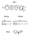
- the clock regeneration circuit essentially consists of three circuit components, namely a clock extraction circuit 1, to which relatively smoothed data pulses are supplied via an incoming data line 2.
- the data pulses are distributed as a random sequence over the temporal locations, which are determined by a signal clock which, as the so-called bit frequency, determines the maximum temporal sequence of the data pulses.
- the clock extraction circuit 1 essentially contains a differentiating element and a rectifier circuit, is connected on the output side to a SAW filter module 3 and supplies it with pulses 4 (compare also FIGS. 2a and 2b) of a relatively short duration, the length of time of these pulses being independent of the bit frequency of the data transmission, i.e. the clock frequency, is always the same.
- the filter module 3 is excited by the output pulses of the module 1 to vibrations that correspond to the clock frequency, so that the clock frequency is available at the output of the filter module 3.
- the vibrations of the filter module 3 are processed so that 5 clock frequency pulses are available at the output of the module, which are suitable for controlling a flip-flop 6.
- the flip-flop 6 also receives the data pulses arriving on line 2 via a line 7, so that the flip-flop 6 is connected to an output 8 Regenerated data pulses can be taken, which are synchronized in phase with the respective time location of a clock pulse.
- the signal clock can also be taken from the module 5 via a line 9.
- Modules 1, 5 and 6 are particularly suitable for this.
- a e.g. The blocks 1, 5 and 6 realizing IC circuit, which is also to be used in regeneration circuits for different clock frequencies, has the disadvantage, however, that as shown in FIGS Data regeneration in module 6 required clock pulses 4 to drive module 6 in the correct phase (FIG. 2a), so that data regeneration in module 6 is effective.
- the temporal position of a regenerated clock pulse 4 compared to a now longer data pulse 11 is unfavorable for an effective regeneration of the data pulse in the module 6 (FIG. 2b).
- the SAW filter module 3 is therefore provided with a phase which is greater, the lower the clock frequency for which the filter module 3 is intended. This is possible, for example, very simply by differently dimensioning the distance between the transmitter electrode configuration and the receiver electrode configuration of the SAW filter module.
- the SAW module 3 which anyway has to be tailored to the respective clock frequency for regeneration circuits which are provided for different clock frequencies, is provided with an increasing phase with decreasing clock frequency.
- a clock pulse 4 which drives the module 6 is thereby always effective at the module 6 in relation to a data pulse 11 in such a way that effective, in-phase data regeneration can be achieved with a circuit arrangement as shown in FIG. 1.
- a controllable load resistor 12 is provided at the output of the filter module 3 (FIG. 3). If a thermistor is used for at least part of the load resistor 3, an undesired change in the phase of the module 3, which is caused by temperature fluctuations, can thereby be compensated for.
Abstract
Description
Die Erfindung bezieht sich auf eine aus wenigstens zwei Taktregenerierschaltungen bestehende Mehrzahl von Regenerierschaltungen, die jeweils für voneinander verschiedene Taktfrequenzen vorgesehen sind und die jeweils wenigstens einen SAW-(surface acoustic wave)-Filterbaustein enthalten, dem ein eingangsseitiger Taktextraktionsschaltkreis aus Datenimpulsen gewonnene Impulse zuführt.The invention relates to a plurality of regeneration circuits consisting of at least two clock regeneration circuits, which are each provided for different clock frequencies and each contain at least one SAW (surface acoustic wave) filter module, to which an input-side clock extraction circuit supplies pulses obtained from data pulses.
Taktregenerierschaltungen werden schon seit längerem mit Hilfe eines Bandpaßfilters realisiert, das von Impulsen, die aus den empfangenen Datenimpulsen abgeleitet werden, gespeist wird. So ist z.B. aus der US-PS 4 004 162 eine Taktregenerierschaltung bekannt, bei der mit Hilfe eines Taktextraktionsschaltkreises, der im wesentlichen aus einem Differenzierglied und einer dem Differenzierglied nachgeschalteten Gleichrichteranordnung besteht, die von der Regenerierschaltung empfangenen Datenimpulse aufbereitet und dann einem Bandpaß zugeführt werden. Der Bandpaß hat eine Mittenfrequenz, die auf die Taktfrequenz der Datenimpulse abgestimmt ist. Durch die Ausgangsimpulse des Taktextraktionsschaltkreises wird der Bandpaß zu Schwingungen angeregt, die die Frequenz des Signaltaktes haben. Aus diesen Schwingungen läßt sich ein Taktsignal gewinnen, mit dessen Hilfe die ankommenden, in der Impulsform verschliffenen Datenimpulse phasenrichtig regeneriert werden können.Clock regeneration circuits have long been realized with the aid of a bandpass filter which is fed by pulses which are derived from the received data pulses. For example, a clock regeneration circuit is known from US Pat. No. 4,004,162, in which, with the aid of a clock extraction circuit which essentially consists of a differentiating element and a rectifier arrangement connected downstream of the differentiating element, the data pulses received by the regenerating circuit are processed and then fed to a bandpass filter. The bandpass has a center frequency that is tuned to the clock frequency of the data pulses. The band-pass filter is excited to oscillations which have the frequency of the signal clock by the output pulses of the clock extraction circuit. A clock signal can be obtained from these oscillations, with the aid of which the incoming data pulses which have been ground in the pulse shape can be regenerated in the correct phase.
Das Bandpaßfilter in einer solchen Taktregenerierschaltung wird neuerdings häufig durch ein SAW-Filter realisiert, das unter Verwendung akustischer Oberflächenwellen arbeitet, vgl. hierzu z.B. IEEE, Journal on Selected Areas in Communications, Vol. SAC-2, No. 6, November 1984, Seiten 957-965.The bandpass filter in such a clock regeneration circuit has recently been frequently implemented by a SAW filter which operates using surface acoustic waves, cf. IEEE, Journal on Selected Areas in Communications, Vol. SAC-2, No. 6, November 1984, pages 957-965.
Außerdem führt der zunehmende Einsatz pulscodierter Datenübertragung, insbesondere auch bei der sogenannten Lichtwellenleiterübertragungstechnik dazu, daß Taktregenerierschaltungen in relativ großer Stückzahl benötigt werden.In addition, the increasing use of pulse-coded data transmission, in particular also in the so-called optical fiber transmission technology, means that clock regeneration circuits are required in relatively large numbers.
Es ist daher Aufgabe vorliegender Erfindung, eine Mehrzahl von Taktregenerierschaltungen der eingangs genannten Art so weiterzubilden, daß die einzelnen Regenerierschaltungen dieser Mehrzahl für voneinander verschiedene Taktfrequenzen auf eine möglichst rationelle Weise hergestellt werden können.It is therefore an object of the present invention to develop a plurality of clock regeneration circuits of the type mentioned at the outset in such a way that the individual regeneration circuits of this plurality can be produced in as rational a manner as possible for different clock frequencies.
Erfindungsgemäß ergibt sich die Lösung dieser Aufgabe dadurch, daß zumindest der Taktextraktionsschaltkreis jeder Regenerierschaltung ein für alle Regenerierschaltungen gleicher IC-Baustein ist, dessen Ausgangsimpulse eine bei allen Regenerierschaltungen gleiche Impulslänge haben, und daß die Filterbausteine für diese Mehrzahl von Regenerierschaltungen eine jeweils in Abhängigkeit von der jeweiligen Taktfrequenz gewählte und mit abnehmender Taktfrequenz zunehmende Phase aufweisen.According to the invention, this object is achieved in that at least the clock extraction circuit of each regeneration circuit is an IC module that is the same for all regeneration circuits, the output pulses of which have the same pulse length for all regeneration circuits, and that the filter modules for this plurality of regeneration circuits each have a function of that have selected clock frequency and increasing with decreasing clock frequency phase.
Dadurch ist es möglich, einen IC-Baustein zu schaffen, der für alle Regenerierschaltungen, ohne Rücksicht darauf, für welche Taktfrequenz die jeweilige Regenerierschaltung vorgesehen ist, immer gleich ist und daher in entsprechend großer Stückzahl produziert werden kann.This makes it possible to create an IC module which is always the same for all regeneration circuits, regardless of the clock frequency for which the respective regeneration circuit is intended, and can therefore be produced in a correspondingly large number.
Zwar werden dadurch dem Filterbaustein stets Impulse gleicher Impulslänge zugeführt. Da aber ein Filterbaustein für eine niedrigere Taktfrequenz mit einer größeren Phase versehen ist, als ein Filterbaustein für eine demgegenüber höhere Taktfrequenz, ergibt sich dennoch keine störende zeitliche Verschiebung der Wirksamkeit der Takt frequenzimpulse bei der Regenerierung der Datenimpulse.In this way, pulses of the same pulse length are always fed to the filter module. However, since a filter module for a lower clock frequency is provided with a larger phase than a filter module for a clock frequency that is higher in comparison, there is nevertheless no disruptive temporal shift in the effectiveness of the clock frequency pulses during the regeneration of the data pulses.
In weiterer Ausgestaltung der Erfindung kann noch vorgesehen sein, daß ein ausgangsseitig des Filterbausteins vorgesehener Lastwiderstand zumindest zum Teil als einstellbarer Widerstand ausgebildet ist und/oder daß der einstellbare Lastwiderstand wenigstens zum Teil als Heißleiter ausgebildet ist.In a further embodiment of the invention it can also be provided that a load resistor provided on the output side of the filter module is at least partially designed as an adjustable resistor and / or that the adjustable load resistor is at least partially configured as a thermistor.
Auf diese Weise ist ein nachträglicher Feinabgleich der Phase des Filterbausteines möglich und mit Hilfe des Heißleiters kann eine unerwünschte temperaturbedingte Phasenänderung kompensiert werden.In this way, a subsequent fine adjustment of the phase of the filter module is possible and with the help of the thermistor, an undesirable temperature-related phase change can be compensated.
Schließlich kann im Rahmen vorliegender Erfindung noch vorgesehen sein, daß der IC-Baustein derart umschaltbar ausgebildet ist, daß die Länge der Ausgangsimpulse des Taktextraktionsschaltkreises stufenweise veränderbar ist.Finally, it can be provided in the context of the present invention that the IC module is designed so that it can be switched over in such a way that the length of the output pulses of the clock extraction circuit can be changed in steps.
Durch diese Auslegung des IC-Bausteins ist es vorteilhaft möglich, die Impulsdauer der Ausgangsimpulse des Taktextraktionsschaltkreises in Stufen umzuschalten, wodurch der IC-Baustein noch besser an unterschiedliche Taktfrequenzen angepaßt werden kann.With this design of the IC module, it is advantageously possible to switch the pulse duration of the output pulses of the clock extraction circuit in stages, as a result of which the IC module can be adapted even better to different clock frequencies.
Nachfolgend werden Ausführungsbeispiele der Erfindung anhand von drei Figuren noch näher erläutert.Exemplary embodiments of the invention are explained in more detail below with reference to three figures.
Dabei zeigen,
- Fig. 1 in Form eines Blockschaltbildes den an sich bekannten Aufbau einer Taktregenerierschaltung,
- Fig. 2a und Fig. 2b jeweils in Diagrammform die zeitlichen Relationen zwischen einem Datenimpuls und einem Taktextraktionsschaltkreis-Ausgangsimpuls, und
- Fig. 3 grob schematisch ein Schaltbild, das die Anordnung eines veränderbaren Lastwiderstandes am Ausgang des Filterbausteines zeigt.
- 1 in the form of a block diagram the known structure of a clock regeneration circuit,
- FIGS. 2a and 2b each show in diagram form the temporal relationships between a data pulse and a clock extraction circuit output pulse, and
- Fig. 3 roughly schematically a circuit diagram showing the arrangement of a variable load resistor at the output of the filter module.
Im einzelnen ist den Figuren zu entnehmen, daß die Taktregenerierschaltung im wesentlichen aus drei Schaltungsbausteinen besteht, nämlich einem Taktextraktionsschaltkreis 1, dem über eine ankommende Datenleitung 2 relativ verschliffene Datenimpulse zugeführt werden. Die Datenimpulse sind als Zufallsfolge auf die zeitlichen Orte verteilt, die durch einen Signaltakt bestimmt werden, der als sogenannte bit-Frequenz die maximale zeitliche Aufeinanderfolge der Datenimpulse bestimmt.In detail, it can be seen from the figures that the clock regeneration circuit essentially consists of three circuit components, namely a
Der Taktextraktionsschaltkreis 1 enthält im wesentlichen ein Differenzierglied und eine Gleichrichterschaltung, ist ausgangsseitig mit einem SAW-Filterbaustein 3 verbunden und liefert diesem Impulse 4 (vergleiche hierzu auch Fig. 2a und Fig. 2b) relativ kurzer Dauer, wobei die zeitliche Länge dieser Impulse unabhängig von der bit-Frequenz der Datenübertragung, also der Taktfrequenz, immer gleich ist.The
Der Filterbaustein 3 wird durch die Ausgangsimpulse des Bausteines 1 zu Schwingungen angeregt, die der Taktfrequenz entsprechen, so daß am Ausgang des Filterbausteines 3 die Taktfrequenz zur Verfügung steht.The
In einer an den Filterbaustein 3 angeschlossenen Verstärker-und/oder Impulsformerstufe 5 werden schließlich die Schwingungen des Filterbausteines 3 so aufbereitet, daß am Ausgang des Bausteines 5 Taktfrequenzimpulse zur Verfügung stehen, die zur Steuerung einer Kippstufe 6 geeignet sind. Der Kippstufe 6 werden außerdem die auf der Leitung 2 ankommenden Datenimpulse über eine Leitung 7 zugeführt, so daß an einem Ausgang 8 der Kippstufe 6 regenerierte Datenimpulse abgenommen werden können, die phasenrichtig auf jeweils den zeitlichen Ort eines Taktimpulses synchronisiert sind. Über eine Leitung 9 kann dem Baustein 5 zusätzlich der Signaltakt entnommen werden.Finally, in an amplifier and / or pulse shaper stage 5 connected to the
Bei der Herstellung einer solchen Schaltung, wie sie in Fig. 1 in Form eines Blockdiagramms dargestellt ist, in rationeller Massenfertigung, ist es wünschenswert, einen Großteil dieser Schaltung in der sogenannten integrierten Schaltungstechnik ausbilden zu können. Hierzu sind insbesondere die Bausteine 1, 5 und 6 geeignet.When producing such a circuit, as shown in FIG. 1 in the form of a block diagram, in rational mass production, it is desirable to be able to design a large part of this circuit in the so-called integrated circuit technology.
Eine z.B. die Bausteine 1, 5 und 6 realisierende IC-Schaltung, die auch bei Regenerierschaltungen für voneinander verschiedene Taktfrequenzen verwendet werden soll, hat jedoch den Nachteil, daß wie die Fig. 2a und 2b zeigen, zwar bei einer Datenübertragung mit einer bestimmten höheren Taktfrequenz die zur Datenregenerierung im Baustein 6 benötigten Taktimpulse 4 den Baustein 6 phasenrichtig ansteuern (Fig. 2a), so daß die Datenregenerierung im Baustein 6 effektiv ist. Dagegen ist bei einer relativ niedrigen Taktfrequenz die zeitliche Lage eines regenerierten Taktimpulses 4 gegenüber einem nun zeitlich längeren Datenimpuls 11 ungünstig für eine effektive Regenerierung des Datenimpulses im Baustein 6 (Fig. 2b).A e.g. The
Der SAW-Filterbaustein 3 ist daher mit einer Phase versehen, die umso größer ist, je niedriger die Taktfrequenz ist, für die der Filterbaustein 3 vorgesehen ist. Dies ist z.B. sehr einfach durch unterschiedliche Bemessung des Abstandes der Sendeelektrodenkonfiguration von der Empfangselektrodenkonfiguration des SAW-Filterbausteines möglich.The
Auf diese Weise ist es möglich, die Bausteine 1, 5 und 6 als eine IC-Schaltung zusammenzufassen, die für Regenerierschaltungen, für unterschiedliche Taktfrequenzen immer gleich ist. Den SAW-Baustein 3, der ohnehin für Regenerierschaltungen, die für unterschiedliche Taktfrequenzen vorgesehen sind, jeweils auf die jeweilige Taktfrequenz zugeschnitten werden muß, versieht man dafür mit einer bei abnehmender Taktfrequenz zunehmenden Phase.In this way it is possible to combine the
Ein den Baustein 6 ansteuernder Taktimpuls 4 wird dadurch in zeitlicher Relation zu einem Datenimpuls 11 immer so am Baustein 6 wirksam, daß eine effektive, phasenrichtige Datenregenerierung mit einer Schaltungsanordnung, wie sie in Fig. 1 dargestellt ist, erzielbar ist.A
Zur Feinabstimmung der Phase des Bausteines 3 ist es vorteilhaft, wenn man einen regelbaren Lastwiderstand 12 am Ausgang des Filterbausteines 3 vorsieht (Fig. 3). Verwendet man zumindest für einen Teil des Lastwiderstandes 3 einen Heißleiter, so kann dadurch eine unerwünschte Änderung der Phase des Bausteines 3, die durch Temperaturschwankungen verursacht wird, kompensiert werden.To fine-tune the phase of the
Claims (4)
Priority Applications (1)
| Application Number | Priority Date | Filing Date | Title |
|---|---|---|---|
| AT87107614T ATE59919T1 (en) | 1986-05-28 | 1987-05-25 | CLOCK RECOVERY CIRCUIT. |
Applications Claiming Priority (2)
| Application Number | Priority Date | Filing Date | Title |
|---|---|---|---|
| DE3617909 | 1986-05-28 | ||
| DE3617909 | 1986-05-28 |
Publications (2)
| Publication Number | Publication Date |
|---|---|
| EP0247569A1 EP0247569A1 (en) | 1987-12-02 |
| EP0247569B1 true EP0247569B1 (en) | 1991-01-09 |
Family
ID=6301779
Family Applications (1)
| Application Number | Title | Priority Date | Filing Date |
|---|---|---|---|
| EP87107614A Expired - Lifetime EP0247569B1 (en) | 1986-05-28 | 1987-05-25 | Clock recovery circuit |
Country Status (7)
| Country | Link |
|---|---|
| US (1) | US4801818A (en) |
| EP (1) | EP0247569B1 (en) |
| JP (1) | JPH0831852B2 (en) |
| AT (1) | ATE59919T1 (en) |
| DE (1) | DE3767214D1 (en) |
| ES (1) | ES2019331B3 (en) |
| GR (1) | GR3001384T3 (en) |
Families Citing this family (7)
| Publication number | Priority date | Publication date | Assignee | Title |
|---|---|---|---|---|
| JP2648928B2 (en) * | 1988-04-28 | 1997-09-03 | 富士重工業株式会社 | Cylinder discriminating apparatus and control method for each cylinder of automobile engine |
| TW242204B (en) * | 1991-12-09 | 1995-03-01 | Philips Nv | |
| JPH08307401A (en) * | 1995-05-10 | 1996-11-22 | Nec Corp | Timing extraction circuit |
| US5870592A (en) * | 1996-10-31 | 1999-02-09 | International Business Machines Corp. | Clock generation apparatus and method for CMOS microprocessors using a differential saw oscillator |
| US6014047A (en) * | 1998-01-07 | 2000-01-11 | International Business Machines Corporation | Method and apparatus for phase rotation in a phase locked loop |
| US5949262A (en) * | 1998-01-07 | 1999-09-07 | International Business Machines Corporation | Method and apparatus for coupled phase locked loops |
| JP2000031889A (en) * | 1998-07-13 | 2000-01-28 | Hitachi Ltd | Mobile communication terminal of spread spectrum communication system |
Family Cites Families (8)
| Publication number | Priority date | Publication date | Assignee | Title |
|---|---|---|---|---|
| FR1603165A (en) * | 1968-07-22 | 1971-03-22 | ||
| US3760111A (en) * | 1970-06-20 | 1973-09-18 | Nippon Electric Co | Pulse regenerative repeater for a multilevel pulse communication system |
| GB1508780A (en) * | 1974-12-18 | 1978-04-26 | Plessey Co Ltd | Circuit for generating synchronisation signals |
| JPS5926136B2 (en) * | 1975-01-25 | 1984-06-25 | 日本電気株式会社 | clock regeneration circuit |
| US3969590A (en) * | 1975-04-04 | 1976-07-13 | Rockwell International Corporation | Surface acoustic wave apparatus |
| US3985970A (en) * | 1975-04-11 | 1976-10-12 | Societe Lignes Telegraphiques Et Telephoniques | Regeneration of signalling pulses |
| DE2951022A1 (en) * | 1979-12-19 | 1981-07-23 | Robert Bosch Gmbh, 7000 Stuttgart | CIRCUIT ARRANGEMENT FOR GENERATING CLOCK PULS IN REGENERATION OF RECTANGLE PULSES |
| GB2128834B (en) * | 1982-10-16 | 1986-01-22 | Ferranti Plc | Circuit that produces long fm pulses |
-
1987
- 1987-05-01 US US07/044,772 patent/US4801818A/en not_active Expired - Fee Related
- 1987-05-25 AT AT87107614T patent/ATE59919T1/en not_active IP Right Cessation
- 1987-05-25 EP EP87107614A patent/EP0247569B1/en not_active Expired - Lifetime
- 1987-05-25 DE DE8787107614T patent/DE3767214D1/en not_active Expired - Fee Related
- 1987-05-25 ES ES87107614T patent/ES2019331B3/en not_active Expired - Lifetime
- 1987-05-28 JP JP62130056A patent/JPH0831852B2/en not_active Expired - Lifetime
-
1991
- 1991-01-28 GR GR90400382T patent/GR3001384T3/en unknown
Also Published As
| Publication number | Publication date |
|---|---|
| GR3001384T3 (en) | 1992-09-11 |
| DE3767214D1 (en) | 1991-02-14 |
| ATE59919T1 (en) | 1991-01-15 |
| JPH0831852B2 (en) | 1996-03-27 |
| US4801818A (en) | 1989-01-31 |
| JPS62290227A (en) | 1987-12-17 |
| ES2019331B3 (en) | 1991-06-16 |
| EP0247569A1 (en) | 1987-12-02 |
Similar Documents
| Publication | Publication Date | Title |
|---|---|---|
| DE10102153B4 (en) | Surface wave device, as well as its use and method for its production | |
| EP1248365A2 (en) | Surface acoustic wave arrangement with at least two surface acoustic wave structures | |
| DE2104779A1 (en) | Band filter circuit | |
| DE102005061601A1 (en) | resonator | |
| EP0247569B1 (en) | Clock recovery circuit | |
| DE102014102707A1 (en) | Tunable RF electroacoustic filter with improved electrical properties and method of operating such a filter | |
| DE102017108105B4 (en) | Filter device for elastic waves | |
| DE2531151C3 (en) | Electromechanical device working with elastic surface waves | |
| DE1962220C3 (en) | Electrostrictively driven tuning fork | |
| DE3604404A1 (en) | NOISE REDUCTION SIGNAL COMPENSATION CIRCUIT | |
| EP0487783B1 (en) | Surface wave resonator | |
| DE2610183A1 (en) | WAVE FILTER WITH ACOUSTIC SURFACE CONDUCTION | |
| DE102016100925A1 (en) | filter circuit | |
| DE2835107C3 (en) | Transducer electrode arrangement for an electromechanical transducer based on the surface wave principle | |
| DE10358347A1 (en) | Surface acoustic wave filter | |
| DE1814954C3 (en) | Electrical filter filter, consisting of two electromechanical filters with different bandwidths | |
| DE1148591B (en) | Clock frequency generator arrangement for pulse code modulation systems | |
| DE2532227A1 (en) | ELECTROMECHANICAL RESONANCE DEVICE AND ITS USE FOR FILTERING TELEVISION SIGNALS | |
| DE2415891A1 (en) | TUNABLE OSCILLATOR | |
| DE4227833C2 (en) | Intermediate frequency filter for a radio receiver | |
| DE2915507C2 (en) | Acoustic wave high frequency oscillator | |
| DE102021212216A1 (en) | High-frequency filter device, high-frequency module and high-frequency filter method | |
| DE2738032C2 (en) | Electromechanical filter | |
| DE3530219C2 (en) | ||
| DE2754026A1 (en) | FILTER DEVICE FOR DETERMINING SEVERAL FREQUENCIES IN AN ELECTRICAL SIGNAL |
Legal Events
| Date | Code | Title | Description |
|---|---|---|---|
| PUAI | Public reference made under article 153(3) epc to a published international application that has entered the european phase |
Free format text: ORIGINAL CODE: 0009012 |
|
| AK | Designated contracting states |
Kind code of ref document: A1 Designated state(s): AT BE CH DE ES FR GB GR IT LI LU NL SE |
|
| 17P | Request for examination filed |
Effective date: 19871218 |
|
| 17Q | First examination report despatched |
Effective date: 19900327 |
|
| GRAA | (expected) grant |
Free format text: ORIGINAL CODE: 0009210 |
|
| AK | Designated contracting states |
Kind code of ref document: B1 Designated state(s): AT BE CH DE ES FR GB GR IT LI LU NL SE |
|
| REF | Corresponds to: |
Ref document number: 59919 Country of ref document: AT Date of ref document: 19910115 Kind code of ref document: T |
|
| REF | Corresponds to: |
Ref document number: 3767214 Country of ref document: DE Date of ref document: 19910214 |
|
| ET | Fr: translation filed | ||
| ITF | It: translation for a ep patent filed |
Owner name: STUDIO JAUMANN |
|
| GBT | Gb: translation of ep patent filed (gb section 77(6)(a)/1977) | ||
| PLBE | No opposition filed within time limit |
Free format text: ORIGINAL CODE: 0009261 |
|
| STAA | Information on the status of an ep patent application or granted ep patent |
Free format text: STATUS: NO OPPOSITION FILED WITHIN TIME LIMIT |
|
| 26N | No opposition filed | ||
| REG | Reference to a national code |
Ref country code: GR Ref legal event code: FG4A Free format text: 3001384 |
|
| PGFP | Annual fee paid to national office [announced via postgrant information from national office to epo] |
Ref country code: AT Payment date: 19940422 Year of fee payment: 8 |
|
| PGFP | Annual fee paid to national office [announced via postgrant information from national office to epo] |
Ref country code: GR Payment date: 19940509 Year of fee payment: 8 |
|
| PGFP | Annual fee paid to national office [announced via postgrant information from national office to epo] |
Ref country code: ES Payment date: 19940512 Year of fee payment: 8 |
|
| PGFP | Annual fee paid to national office [announced via postgrant information from national office to epo] |
Ref country code: BE Payment date: 19940520 Year of fee payment: 8 |
|
| PGFP | Annual fee paid to national office [announced via postgrant information from national office to epo] |
Ref country code: SE Payment date: 19940526 Year of fee payment: 8 |
|
| PGFP | Annual fee paid to national office [announced via postgrant information from national office to epo] |
Ref country code: NL Payment date: 19940531 Year of fee payment: 8 Ref country code: LU Payment date: 19940531 Year of fee payment: 8 |
|
| EPTA | Lu: last paid annual fee | ||
| EAL | Se: european patent in force in sweden |
Ref document number: 87107614.7 |
|
| PGFP | Annual fee paid to national office [announced via postgrant information from national office to epo] |
Ref country code: FR Payment date: 19950522 Year of fee payment: 9 |
|
| PG25 | Lapsed in a contracting state [announced via postgrant information from national office to epo] |
Ref country code: LU Free format text: LAPSE BECAUSE OF NON-PAYMENT OF DUE FEES Effective date: 19950525 Ref country code: AT Effective date: 19950525 |
|
| PG25 | Lapsed in a contracting state [announced via postgrant information from national office to epo] |
Ref country code: SE Effective date: 19950526 Ref country code: ES Free format text: LAPSE BECAUSE OF NON-PAYMENT OF DUE FEES Effective date: 19950526 |
|
| PG25 | Lapsed in a contracting state [announced via postgrant information from national office to epo] |
Ref country code: BE Effective date: 19950531 |
|
| PGFP | Annual fee paid to national office [announced via postgrant information from national office to epo] |
Ref country code: CH Payment date: 19950817 Year of fee payment: 9 |
|
| BERE | Be: lapsed |
Owner name: SIEMENS A.G. Effective date: 19950531 |
|
| PG25 | Lapsed in a contracting state [announced via postgrant information from national office to epo] |
Ref country code: GR Free format text: THE PATENT HAS BEEN ANNULLED BY A DECISION OF A NATIONAL AUTHORITY Effective date: 19951130 |
|
| PG25 | Lapsed in a contracting state [announced via postgrant information from national office to epo] |
Ref country code: NL Effective date: 19951201 |
|
| REG | Reference to a national code |
Ref country code: GR Ref legal event code: MM2A Free format text: 3001384 |
|
| NLV4 | Nl: lapsed or anulled due to non-payment of the annual fee |
Effective date: 19951201 |
|
| EUG | Se: european patent has lapsed |
Ref document number: 87107614.7 |
|
| PG25 | Lapsed in a contracting state [announced via postgrant information from national office to epo] |
Ref country code: LI Effective date: 19960531 Ref country code: CH Effective date: 19960531 |
|
| REG | Reference to a national code |
Ref country code: CH Ref legal event code: PL |
|
| PG25 | Lapsed in a contracting state [announced via postgrant information from national office to epo] |
Ref country code: FR Effective date: 19970131 |
|
| REG | Reference to a national code |
Ref country code: FR Ref legal event code: ST |
|
| PGFP | Annual fee paid to national office [announced via postgrant information from national office to epo] |
Ref country code: GB Payment date: 19970418 Year of fee payment: 11 |
|
| PGFP | Annual fee paid to national office [announced via postgrant information from national office to epo] |
Ref country code: DE Payment date: 19970721 Year of fee payment: 11 |
|
| PG25 | Lapsed in a contracting state [announced via postgrant information from national office to epo] |
Ref country code: GB Free format text: LAPSE BECAUSE OF NON-PAYMENT OF DUE FEES Effective date: 19980525 |
|
| GBPC | Gb: european patent ceased through non-payment of renewal fee |
Effective date: 19980525 |
|
| PG25 | Lapsed in a contracting state [announced via postgrant information from national office to epo] |
Ref country code: DE Free format text: LAPSE BECAUSE OF NON-PAYMENT OF DUE FEES Effective date: 19990302 |
|
| REG | Reference to a national code |
Ref country code: ES Ref legal event code: FD2A Effective date: 19990301 |
|
| PG25 | Lapsed in a contracting state [announced via postgrant information from national office to epo] |
Ref country code: IT Free format text: LAPSE BECAUSE OF NON-PAYMENT OF DUE FEES Effective date: 20050525 |