EP0246626B1 - Akustische Oberflächenwellenanordnung - Google Patents
Akustische Oberflächenwellenanordnung Download PDFInfo
- Publication number
- EP0246626B1 EP0246626B1 EP87107300A EP87107300A EP0246626B1 EP 0246626 B1 EP0246626 B1 EP 0246626B1 EP 87107300 A EP87107300 A EP 87107300A EP 87107300 A EP87107300 A EP 87107300A EP 0246626 B1 EP0246626 B1 EP 0246626B1
- Authority
- EP
- European Patent Office
- Prior art keywords
- layer
- added
- saw device
- electrodes
- impurity
- Prior art date
- Legal status (The legal status is an assumption and is not a legal conclusion. Google has not performed a legal analysis and makes no representation as to the accuracy of the status listed.)
- Expired
Links
Images

Classifications
-
- H—ELECTRICITY
- H03—ELECTRONIC CIRCUITRY
- H03H—IMPEDANCE NETWORKS, e.g. RESONANT CIRCUITS; RESONATORS
- H03H3/00—Apparatus or processes specially adapted for the manufacture of impedance networks, resonating circuits, resonators
- H03H3/007—Apparatus or processes specially adapted for the manufacture of impedance networks, resonating circuits, resonators for the manufacture of electromechanical resonators or networks
- H03H3/08—Apparatus or processes specially adapted for the manufacture of impedance networks, resonating circuits, resonators for the manufacture of electromechanical resonators or networks for the manufacture of resonators or networks using surface acoustic waves
-
- H—ELECTRICITY
- H03—ELECTRONIC CIRCUITRY
- H03H—IMPEDANCE NETWORKS, e.g. RESONANT CIRCUITS; RESONATORS
- H03H9/00—Networks comprising electromechanical or electro-acoustic elements; Electromechanical resonators
- H03H9/02—Details
- H03H9/02535—Details of surface acoustic wave devices
- H03H9/02818—Means for compensation or elimination of undesirable effects
- H03H9/02929—Means for compensation or elimination of undesirable effects of ageing changes of characteristics, e.g. electro-acousto-migration
-
- H—ELECTRICITY
- H03—ELECTRONIC CIRCUITRY
- H03H—IMPEDANCE NETWORKS, e.g. RESONANT CIRCUITS; RESONATORS
- H03H9/00—Networks comprising electromechanical or electro-acoustic elements; Electromechanical resonators
- H03H9/02—Details
- H03H9/125—Driving means, e.g. electrodes, coils
- H03H9/145—Driving means, e.g. electrodes, coils for networks using surface acoustic waves
- H03H9/14538—Formation
- H03H9/14541—Multilayer finger or busbar electrode
Definitions
- the present invention generally relates to a surface acoustic wave device (hereinafter referred to as SAW device in abbreviation). More particularly, the invention concerns a SAW device capable of handling electric signals of high power and/or a large amplitude.
- SAW device surface acoustic wave device
- the SAW device finds a wide range of utilization and application and is employed as a SAW filter adapted for transmission of high electric power or as a SAW resonator in which surface wave of a large amplitude is continuously present as a standing wave.
- the SAW devices mentioned above suffer short-comings in that defects similar to hillocks, voids or the like due to electro-migration which take plate in Al-metallized electrodes in semiconductor IC devices are produced in fine fingers of aluminum (Al) serving as SAW transmission/reception electrodes and reflector electrodes in the SAW devices, as is reported in "Thin Solid Films", 64, 9-15 (1979) (J. I. Latham et al), pp.
- the second mentioned literature explains the generating mechanism of such failure as follows: "Strain in a substrate surface produced by the SAW induces an internal stress in the Al-thin film formed on the substrate surface, as a result of which Al-crystalline grain boundary migrats in a region where the stress exceeds a threshold, giving rise to creation of the voids and hillocks.
- the migration of the grain boundary is believed to be ascribable to such mechanism as experienced in the thermal cycle of ICs, as reported in IEEE Trans, Parts, Hybrids and Packaging, Vol. PHP-7, pp. 134 - 138, Sept 1971".
- the first to third literatures mentioned above disclose that the failures due to Al-migration can be dealt with by adding a small amount (1 to 4 wt. %) of copper (Cu) to Al forming the conductors in the semiconductor ICs and that this method is effective for suppressing the migration.
- the wiring in a semiconductor IC is of a multilayer comprising a first layer of an Al film which is added with Cu as impurity and a second layer of, for example, a hafnium (Hf) film which is exclusive of Al and much thinner than the first Al film layer.
- Hf hafnium
- a SAW device in which electrodes are formed on a piezoelectric substrate by sputtering and/or the electrodes contain an additive of Cu, Ti, Zn, Mg, Fe, Ni, Cr, Ga, Ge, Sn, Pd or Ta.
- An object of the present invention is to provide a highly reliable SAW device which can sustain its operation for a long period of time even when a high power (large amplitude) SAW is applied to the SAW device.
- At least one of electrodes for excitation, propagation and reflection of a SAW has a laminated structure including a first layer of an Al film which is either made of pure Al or made of Al added with a first impurity at a low concentration and a second layer of an Al film which is disposed in laminated relationship with the first layer and added with a second impurity at a low concentration.
- the first impurity any one of titanium (Ti), copper (Cu), magnesium (Mg), zinc (Zn) and nickel (Ni) may be used and as the second impurity, any one of titanium, chronium (Cr), vanadium (V) and manganese (Mn) may be used.
- the second layer of the electrodes is simply a film of Ti alone, then this second layer of Ti will become a powerful Ti diffusion source for the Al film of the first layer. Accordingly, when a SAW device with such an electrode structure is operated for a long period of time at a high temperature, Al in the first layer and Ti in the second layer will almost alloy together. Consequently, in an instance where the ratio of film thickness between the first and second layers is 99 : 1, resistivity of the electrodes being originally 2.72 ⁇ cm is considerably increased up to 5.8 ⁇ cm after the alloying. Such a SAW device is therefore impractical.
- an electrode structure exemplarily comprises a second layer of an Al film added with Ti in 2 wt. % and a first layer of a pure Al film (for example, with the ratio of film thicknesses there between being 9 : 1) in accordance with an embodiment of the present invention
- an increase in resistivity of the electrodes being originally 2.9 ⁇ cm can be suppressed to 3.3 ⁇ cm even if Al in the first layer and Ti in the second layer supposedly alloy together. This suppressed increase is not of practical adversities.
- the second layer having the Al film added with Ti as in one embodiment of the present invention has no substantial ability to act as a Ti diffusion source for the first layer so that the first and second layers are difficult to alloy together.
- Ti in the second layer is, in practice, selectively trapped at the most in an Al crystalline grain boundary, feasible to diffuse, in the first layer and no appreciable degradation (increase) with time of the resistivity will occur.
- the second layer in the form of the Al film added with Ti in 2 wt. % has a migration-proof characteristic which is superior to that of the second layer of Ti alone, indicating that the overall second layer effectively suppresses the occurrence of hillocks, voids and the like due to electro-migration in the first layer.
- the Ti selectively trapped in the Al crystalline grain boundary in the first layer can suppress diffusion of the grain boundary of Al atoms and for this reason the first layer can by itself improve migration-proof characteristic. For all reasons described above, reliability of the SAW device under the application of a high power SAW can be improved considerably.
- a material having a good migration-proof characteristic even though exhibiting a large resistivity in itself or when added to Al, is added by a small amount to the Al film of the second layer to thereby decrease initial resistivity of the electrodes.
- a change with time in the resistivity of the electrodes is suppressed and reliability of the SAW device is improved.
- Fig. 1 is a perspective view showing a SAW device according to an exemplary embodiment of the present invention.
- Fig. 2 is a view showing a cross-section taken along the line II-II in Fig. 1.
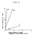
- Fig. 3 is a characteristic diagram illustrating results of an accelerated life test conducted on an apparatus according to an embodiment of the invention and incorporating the SAW device shown in Figs. 1 and 2.
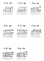
- Fig. 4a is a partial enlarged sectional view showing a part of electrodes of the SAW device shown in Figs. 1 and 2.
- Figs. 4b to 4h are partial enlarged sectional views showing various modifications of a part of electrodes according to the invention.
- Fig. 1 shows, in perspective view, a SAW device according to an embodiment of the invention and Fig. 2 shows a section taken on the line II-II of Fig. 1.
- a reference numeral 1 denotes a piezoelectric SAW substrate formed of ST-cut quartz crystal on which a pair of transmitting and receiving electrode arrays 2 and 2 ⁇ are disposed, each array including 28 pairs of fingers with aperture thereof being 1000 ⁇ m for mutually transmitting and receiving SAW.
- the electrodes are connected to bonding pads 3, 3 ⁇ by way of bus electrodes, while the bonding pads 3, 3 ⁇ are electrically connected to input/output pins 4 and 4 ⁇ of a stem of a can package by means of bonding wires of Al or Au.
- Each of the pair of electrodes 2 and 2 ⁇ includes one set of interleaved comb-like finger electrodes. Disposed on both sides of the aforementioned pair of transmitting/receiving electrodes 2 and 2 ⁇ are reflector electrodes 5 and 5 ⁇ composed of 750 metallic strips to thereby constitute a two-port SAW resonator. In the version of this embodiment, the metallic strips 5 may be replaced by slits formed in the substrate 1 serving as the reflectors.
- Each of the aforementioned transmitting/receiving electrodes 2, 2 ⁇ and the reflector electrodes has a film thickness of 0.1 ⁇ m.
- each of the electrodes is of a two-layer structure comprising a first layer 7 and a second layer 8. A part of the electrode is illustrated, in enlarged sectional view form, in Fig. 4a.
- the first layer 7 is made of pure Al, having a film thickness of 0.08 ⁇ m.
- the second layer 8 is made of Al added with Ti in 2 wt. % and has a film thickness of 0.02 ⁇ m.
- the electrodes each comprised of the first and second layers was deposited by DC magnetron sputtering which is best suited for this type of metallic film among various sputtering methods. After deposition of the film, the electrode pattern was formed through photoetching process.
- results of an accelerated life test conducted on the saw resonators according to the instant embodiment are graphically illustrated in Fig. 3 comparatively with a result obtained from a specimen manufactured by EB evaporation of Cu-added Al.
- abscissa represents a mean content or concentration, in terms of wt. %, of Ti added to the second layer which is averaged over the overall electrode comprised of the first and second layers.
- the second layer is added by itself with Ti at a concentration of 2 wt. %, the Ti concentration becomes 0.4 wt. % for the overall electrode.
- the film thickness of the second layer shares 0.02 ⁇ m in the film thickness of the overall electrode being 0.1 ⁇ m and the Ti concentration in the second layer can be converted into a concentration as viewed from the overall electrode by being multiplied by 1/5.
- Represented by abscissa in Fig. 3 is a concentration converted into a mean concentration for the overall electrode.
- Ordinate represents time to failure (TF). The time to failure indicates the time elapse until the resonance frequency is degraded to change.
- the conditions for the accelerated life test are selected such that the temperature is 120°C and that the input power is 100 mW.
- TF time to failure
- a curve 11 represents experimental results on a comparative specimen prepared through conventional EB evaporation of Cu-added Al
- a curve 9 represents experimental results on a specimen prepared in accordance with the present embodiment
- a curve 10 represents experimental results on a specimen in which the electrode is the same as that of the present embodiment in respect of configuration, thickness and the way of formation but the two-layer structure is replaced with a single layer structure of an Al film added with Ti over the overall electrode.
- curve 10 is not representative of data for a prior art example but is representative of data for comparison with the present embodiment from the effect achieving point of view.
- a SAW device having a TF of 8 hours or more can be obtained at a Ti mean concentration of 0.4 wt. % (2 wt. % Ti concentration in the second layer) on curve 9 according to the present embodiment, and a SAW device having a TF of 5 hours or less can be obtained at a Ti mean concentration of 0.2 wt. % (1 wt. % Ti concentration in the second layer) on curve 9. No degradation in frequency characteristic is found in both the SAW device.
- curve 9 shows that the present embodiment (curve 9) can prolong the life by adding Ti to the electrode at a lower Ti mean concentration than that required for the example represented by curve 10.
- electrical resistivity of the electrodes is 3.3 ⁇ cm with no appreciable degradation (increase) with time, indicating no practical adversities in respect of the resistivity and degradation with time.
- the dimensions such that the overall electrode thickness is 0.1 ⁇ m and the film thickness of the second layer is 0.02 ⁇ m in the foregoing embodiment are in no way limitative.
- the film thickness of the second layer be about 50% of the overall electrode thickness at the most.
- the film thickness of the second layer be 1% or more of the overall electrode thickness.
- the amount of Ti added to the Al film of the second layer in the present embodiment should preferably be about 6 wt. % at the most because an excessively high concentration hardens the Al film excessively.
- Ti is added as inpurity to the second layer in the present embodiment but the impurity is not limited to Ti and an additive of Cr, V or Mn may be used to attain similar effects.
- the pure Al film used as the first layer in the present embodiment may be added with an impurity to further prolong the life of the SAW device, so long as the resistivity will not increase.
- the additive impurity is Ti, Cu, Mg, Zn or Ni. Because of the requirement that the film resistivity be 5 ⁇ cm or less, the amount of additive impurity is 0.4 wt. % or less. Thus, a small amount (about 0.4 wt. % or less) of the impurity may be added to the layer of low resistivity.
- the laminated structure is such that the first layer 7 of pure Al is next to the piezoelectric SAW substrate 1 and the second layer 8 added with an impurity overlies the first layer, as illustrated in Figs. 2 and 4a, but this lamination is not limitative.
- the laminated relationship may be reversed without disturbing the effects described previously, so that the second layer 8 may be contiguous to the piezoelectric SAW substrate 1 and the first layer 7 may overlie the second layer 8.
- a modification to this effect is illustrated in Fig. 4b.
- the electrodes directed to this modification a part of which is shown in enlarged sectional form in Fig. 4b, are the same as the Fig.
- a first layer means a layer made of Al or Al added with a first impurity
- a second layer means a layer made of Al added with a second impurity. This also applies to the following description.
- Figs. 4c to 4h show a part thereof in enlarged sectional form.
- the electrodes directed to these modifications are the same as the Fig. 1 embodiment in respect of configuration and array pattern, excepting lamination structures.
- the modification of Fig. 4c is of a three-layer structure in which a second layer 8 is disposed on a sub-layer 7a and a sub-layer 7b of the same material as that of the sub-layer 7a is disposed on the second layer 8.
- the sub-layers 7a and 7b constitute a first layer. This modification can attain similar effects to those of the Fig. 4a embodiment.
- a first layer 7 is disposed on sub-layer 8a of a second layer and a sub-layer 8b of the second layer is disposed on the first layer 7.
- a first layer comprises a sub-layer 7a, and a sub-layer 7b which overlies the sub-layer 7a and differs therefrom in properties by, for example, containing Al added with an impurity by an amount different from that for the sub-layer 7a, and a second layer 8 is disposed on the sub-layer 7b.
- a sub-layer 8a of a second layer is disposed on a first layer 7 and there is disposed on the sub-layer 8a a sub-layer 8b of the second layer which differs from the sub-layer 8a in properties by, for example, containing Al added with an impurity by an amount different from that for the sub-layer 8a.
- a first layer comprises sub-layers 7a and 7b
- a second layer comprises sub-layers 8a and 8b
- the sub-layers 7a, 8a, 7b and 8b are laminated in this order.
- a first layer comprises sub-layers 7a and 7b
- a second layer comprises sub-layers 8a and 8b
- the sub-layers 7a, 7b, 8a and 8b are laminated in this order, the sub-layer 7b being different from the sub-layer 7a in properties and the sub-layer 8b being different from the sub-layer 8a in properties.
- the laminated structure of electrodes may be configured into a three-layer structure and a four-layer structure without disturbing the effects of the invention described hereinbefore.
- the number of laminated layers may be increased to five or more.
- the two-layer structure of electrodes may also be prepared by initially forming a first layer 7 and thereafter diffusing Ti into the surface of the first layer 7 to convert an upper portion of the first layer 7 into a second layer 8. In this case, the boundary between the first layer 7 and the second layer 8 is indistinctive.
- Fig. 1 Although the embodiment of the invention described in connection with Fig. 1 is directed to a two-port SAW resonator having reflectors formed of metallic strips, the invention is not limited thereto and may be applied, without disturbing its achievable effects, to a one-port SAW resonator and a SAW filter for high power transmission from input electrodes to output electrodes as well as a resonator using a SAW transmitter/receiver.
- the SAW substrate is not limited to the ST-cut quartz crystal but other types of various substrates with various cut orientations may effectively be used, including LiNbO3, LiTaO3 and the like.
Landscapes
- Physics & Mathematics (AREA)
- Acoustics & Sound (AREA)
- Engineering & Computer Science (AREA)
- Manufacturing & Machinery (AREA)
- Surface Acoustic Wave Elements And Circuit Networks Thereof (AREA)
Claims (9)
- Akustische Oberflächenwellenanordnung mit einem piezoelektrischen Substrat (1) und Sätzen von Fingerelektroden (2, 2', 5, 5'), die auf dem piezoelektrischen Substrat angeordnet sind, wobei mindestens ein Satz der Elektroden eine laminierte Struktur aufweist, einschließlich einer ersten Schicht (7) eines Aluminiumfilms und einer zweiten Schicht (8) eines Aluminiumfilms, der in laminierter Beziehung zu der ersten Schicht angeordnet ist und dem eine Verunreinigung zugefügt ist.
- Akustische Oberflächenwellenanordnung nach Anspruch 1, wobei der zweiten Schicht die Verunreinigung mit einer Konzentration von 6 Gew.-% oder weniger hinzugefügt ist.
- Akustische Oberflächenwellenanordnung nach Anspruch 1, wobei die Verunreinigung, die der zweiten Schicht hinzugefügt ist, aus der Gruppe ausgewählt ist, die aus Titan, Chrom, Vanadium und Mangan besteht.
- Akustische Oberflächenwellenanordnung nach Anspruch 2, wobei die Verunreinigung, die der zweiten Schicht hinzugefügt ist, aus der Gruppe ausgewählt ist, die aus Titan, Chrom, Vanadium und Mangan besteht.
- Akustische Oberflächenwellenanordnung nach Anspruch 1, wobei dem Aluminiumfilm der ersten Schicht eine Verunreinigung hinzugefügt ist, die aus der Gruppe ausgewählt ist, die aus Titan, Kupfer, Magnesium, Zink und Nickel besteht, und zwar mit einer Konzentration von 0,4 Gew.-% oder weniger.
- Akustische Oberflächenwellenanordnung nach Anspruch 2, wobei dem Aluminiumfilm der ersten Schicht eine Verunreinigung hinzugefügt ist, die aus der Gruppe ausgewählt ist, die aus Titan, Kupfer, Magnesium, Zink und Nickel besteht, und zwar mit einer Konzentration von 0,4 Gew.-% oder weniger.
- Akustische Oberflächenwellenanordnung nach Anspruch 3, wobei dem Aluminiumfilm der ersten Schicht eine Verunreinigung hinzugefügt ist, die aus der Gruppe ausgewählt ist, die aus Titan, Kupfer, Magnesium, Zink und Nickel besteht, und zwar mit einer Konzentration von 0,4 Gew.-% oder weniger.
- Akustische Oberflächenwellenanordnung nach Anspruch 4, wobei dem Aluminiumfilm der ersten Schicht eine Verunreinigung hinzugefügt ist, die aus der Gruppe ausgewählt ist, die aus Titan, Kupfer, Magnesium, Zink und Nickel besteht, und zwar mit einer Konzentration von 0,4 Gew.-% oder weniger.
- Akustische Oberflächenwellenanordnung nach Anspruch 1, wobei die gesamte Filmdecke der ersten Schicht größer als jene der zweiten Schicht ist.
Applications Claiming Priority (2)
| Application Number | Priority Date | Filing Date | Title |
|---|---|---|---|
| JP114540/86 | 1986-05-21 | ||
| JP61114540A JPS62272610A (ja) | 1986-05-21 | 1986-05-21 | 弾性表面波素子 |
Publications (3)
| Publication Number | Publication Date |
|---|---|
| EP0246626A2 EP0246626A2 (de) | 1987-11-25 |
| EP0246626A3 EP0246626A3 (en) | 1989-03-08 |
| EP0246626B1 true EP0246626B1 (de) | 1992-05-06 |
Family
ID=14640318
Family Applications (1)
| Application Number | Title | Priority Date | Filing Date |
|---|---|---|---|
| EP87107300A Expired EP0246626B1 (de) | 1986-05-21 | 1987-05-19 | Akustische Oberflächenwellenanordnung |
Country Status (4)
| Country | Link |
|---|---|
| US (1) | US4775814A (de) |
| EP (1) | EP0246626B1 (de) |
| JP (1) | JPS62272610A (de) |
| DE (1) | DE3778754D1 (de) |
Families Citing this family (29)
| Publication number | Priority date | Publication date | Assignee | Title |
|---|---|---|---|---|
| GB2186456B (en) * | 1986-01-13 | 1989-11-08 | Hitachi Ltd | Surface acoustic wave device |
| JPS6480113A (en) * | 1987-09-22 | 1989-03-27 | Hitachi Ltd | Surface acoustic wave device |
| JPH01303910A (ja) * | 1988-06-01 | 1989-12-07 | Hitachi Ltd | 固体電子素子、その製造方法、及びそれを利用した装置 |
| US5162690A (en) * | 1989-04-14 | 1992-11-10 | Murata Manufacturing Co., Ltd. | Surface acoustic wave device |
| JPH0314305A (ja) * | 1989-06-13 | 1991-01-23 | Murata Mfg Co Ltd | 弾性表面波装置の製造方法 |
| JPH0340510A (ja) * | 1989-07-06 | 1991-02-21 | Murata Mfg Co Ltd | 弾性表面波装置 |
| US5039957A (en) * | 1990-05-07 | 1991-08-13 | Raytheon Company | High power surface acoustic wave devices having copper and titanium doped aluminum transducers and long-term frequency stability |
| JP2733006B2 (ja) | 1993-07-27 | 1998-03-30 | 株式会社神戸製鋼所 | 半導体用電極及びその製造方法並びに半導体用電極膜形成用スパッタリングターゲット |
| JP3379049B2 (ja) * | 1993-10-27 | 2003-02-17 | 富士通株式会社 | 表面弾性波素子とその製造方法 |
| JPH0969748A (ja) * | 1995-09-01 | 1997-03-11 | Matsushita Electric Ind Co Ltd | Sawデバイスおよびその製造方法 |
| JP3609423B2 (ja) * | 1995-09-21 | 2005-01-12 | Tdk株式会社 | 弾性表面波装置及びその製造方法 |
| JPH09223944A (ja) * | 1995-12-13 | 1997-08-26 | Fujitsu Ltd | 弾性表面波素子及びその製造方法 |
| CN1133268C (zh) * | 1997-07-28 | 2003-12-31 | 东芝株式会社 | 表面声波滤波器及其制造方法 |
| JP3266109B2 (ja) * | 1998-08-05 | 2002-03-18 | 株式会社村田製作所 | 電子デバイスの作製方法 |
| US6259185B1 (en) * | 1998-12-02 | 2001-07-10 | Cts Corporation | Metallization for high power handling in a surface acoustic wave device and method for providing same |
| JP3338010B2 (ja) * | 1999-10-18 | 2002-10-28 | 富士通株式会社 | 弾性表面波素子及びその製造方法 |
| US6452305B1 (en) * | 2000-03-14 | 2002-09-17 | Motorola, Inc. | High power surface acoustic wave device |
| JP3402311B2 (ja) * | 2000-05-19 | 2003-05-06 | 株式会社村田製作所 | 弾性表面波装置 |
| EP2458735A3 (de) * | 2000-10-23 | 2012-08-29 | Panasonic Corporation | Oberflächenwellenfilter |
| JP3445971B2 (ja) * | 2000-12-14 | 2003-09-16 | 富士通株式会社 | 弾性表面波素子 |
| DE10206480B4 (de) | 2001-02-16 | 2005-02-10 | Leibniz-Institut für Festkörper- und Werkstoffforschung e.V. | Akustisches Oberflächenwellenbauelement |
| US6965190B2 (en) * | 2001-09-12 | 2005-11-15 | Sanyo Electric Co., Ltd. | Surface acoustic wave device |
| US7148610B2 (en) * | 2002-02-01 | 2006-12-12 | Oc Oerlikon Balzers Ag | Surface acoustic wave device having improved performance and method of making the device |
| DE10206369B4 (de) * | 2002-02-15 | 2012-12-27 | Epcos Ag | Elektrodenstruktur mit verbesserter Leistungsverträglichkeit und Verfahren zur Herstellung |
| JP3774782B2 (ja) * | 2003-05-14 | 2006-05-17 | 富士通メディアデバイス株式会社 | 弾性表面波素子の製造方法 |
| CN101395296B (zh) | 2006-03-06 | 2012-03-28 | 陶斯摩有限公司 | 溅射靶 |
| KR20080100358A (ko) * | 2006-03-06 | 2008-11-17 | 토소우 에스엠디, 인크 | 전자 장치, 이의 제조방법 및 스퍼터링 타겟 |
| AT509633A1 (de) * | 2010-03-29 | 2011-10-15 | Ctr Carinthian Tech Res Ag | Hochtemperaturbeständige, elektrisch leitfähige dünnschichten |
| US12081199B2 (en) * | 2022-01-13 | 2024-09-03 | Rf360 Singapore Pte. Ltd. | Surface acoustic wave (SAW) device with one or more intermediate layers for self-heating improvement |
Family Cites Families (4)
| Publication number | Priority date | Publication date | Assignee | Title |
|---|---|---|---|---|
| GB1580600A (en) * | 1978-05-09 | 1980-12-03 | Philips Electronic Associated | Kpiezoelectric devices |
| DE3117747A1 (de) * | 1981-05-05 | 1982-11-25 | Kollsman System-Technik GmbH, 8000 München | Piezoelektrisches element |
| JPS594310A (ja) * | 1982-06-30 | 1984-01-11 | Toshiba Corp | 弾性表面波装置 |
| JPH0773177B2 (ja) * | 1984-12-17 | 1995-08-02 | 株式会社東芝 | 弾性表面波共振子 |
-
1986
- 1986-05-21 JP JP61114540A patent/JPS62272610A/ja active Pending
-
1987
- 1987-05-19 DE DE8787107300T patent/DE3778754D1/de not_active Expired - Lifetime
- 1987-05-19 EP EP87107300A patent/EP0246626B1/de not_active Expired
- 1987-05-19 US US07/051,523 patent/US4775814A/en not_active Expired - Fee Related
Also Published As
| Publication number | Publication date |
|---|---|
| EP0246626A2 (de) | 1987-11-25 |
| US4775814A (en) | 1988-10-04 |
| EP0246626A3 (en) | 1989-03-08 |
| JPS62272610A (ja) | 1987-11-26 |
| DE3778754D1 (de) | 1992-06-11 |
Similar Documents
| Publication | Publication Date | Title |
|---|---|---|
| EP0246626B1 (de) | Akustische Oberflächenwellenanordnung | |
| EP2175556B1 (de) | Elastische Wellenvorrichtung und Herstellungsverfahren dafür | |
| US7602099B2 (en) | Surface acoustic wave device and method of manufacturing the same | |
| KR930000882B1 (ko) | 고체 전자소자 | |
| USRE38002E1 (en) | Process for providing a surface acoustic wave device | |
| KR100312001B1 (ko) | 탄성표면파장치 | |
| US7459991B2 (en) | SAW component having an improved temperature coefficient | |
| US5144185A (en) | SAW device | |
| US7692515B2 (en) | Low-loss electro-acoustic component | |
| EP0392879B1 (de) | Akustische Oberflächenwellenanordnung | |
| US12176879B2 (en) | Acoustic wave device, filter and multiplexer | |
| JPH06350377A (ja) | 弾性表面波素子 | |
| JP3659455B2 (ja) | 弾性表面波装置 | |
| JP2555072B2 (ja) | 固体電子装置 | |
| JP7709807B2 (ja) | 弾性波共振器、フィルタ、およびマルチプレクサ | |
| JP2019192994A (ja) | 弾性波共振器、フィルタおよびマルチプレクサ | |
| JPH01128607A (ja) | 弾性表面波装置 | |
| JPS62295504A (ja) | 弾性表面波装置 | |
| JPS62163408A (ja) | 弾性表面波装置 | |
| CN223729721U (zh) | 弹性波器件及模块 | |
| JP3296097B2 (ja) | 弾性表面波素子 | |
| CN120856088A (zh) | 弹性波器件、滤波器以及多路复用器 | |
| JPH02274008A (ja) | 固体電子装置、その製造方法、及びそれを利用した装置 | |
| JPH043510A (ja) | 極薄・耐マイグレーション電極 | |
| WO2025022906A1 (ja) | フィルタ装置 |
Legal Events
| Date | Code | Title | Description |
|---|---|---|---|
| PUAI | Public reference made under article 153(3) epc to a published international application that has entered the european phase |
Free format text: ORIGINAL CODE: 0009012 |
|
| 17P | Request for examination filed |
Effective date: 19870519 |
|
| AK | Designated contracting states |
Kind code of ref document: A2 Designated state(s): DE GB |
|
| PUAL | Search report despatched |
Free format text: ORIGINAL CODE: 0009013 |
|
| AK | Designated contracting states |
Kind code of ref document: A3 Designated state(s): DE GB |
|
| 17Q | First examination report despatched |
Effective date: 19910722 |
|
| GRAA | (expected) grant |
Free format text: ORIGINAL CODE: 0009210 |
|
| AK | Designated contracting states |
Kind code of ref document: B1 Designated state(s): DE GB |
|
| REF | Corresponds to: |
Ref document number: 3778754 Country of ref document: DE Date of ref document: 19920611 |
|
| PGFP | Annual fee paid to national office [announced via postgrant information from national office to epo] |
Ref country code: DE Payment date: 19920623 Year of fee payment: 6 |
|
| PG25 | Lapsed in a contracting state [announced via postgrant information from national office to epo] |
Ref country code: GB Effective date: 19920806 |
|
| PLBE | No opposition filed within time limit |
Free format text: ORIGINAL CODE: 0009261 |
|
| STAA | Information on the status of an ep patent application or granted ep patent |
Free format text: STATUS: NO OPPOSITION FILED WITHIN TIME LIMIT |
|
| GBPC | Gb: european patent ceased through non-payment of renewal fee |
Effective date: 19920806 |
|
| 26N | No opposition filed | ||
| PG25 | Lapsed in a contracting state [announced via postgrant information from national office to epo] |
Ref country code: DE Effective date: 19940201 |