EP0245886A2 - Circuit pour un dispositif de reproduction d'images - Google Patents
Circuit pour un dispositif de reproduction d'images Download PDFInfo
- Publication number
- EP0245886A2 EP0245886A2 EP87200605A EP87200605A EP0245886A2 EP 0245886 A2 EP0245886 A2 EP 0245886A2 EP 87200605 A EP87200605 A EP 87200605A EP 87200605 A EP87200605 A EP 87200605A EP 0245886 A2 EP0245886 A2 EP 0245886A2
- Authority
- EP
- European Patent Office
- Prior art keywords
- frequency
- amplitude limiter
- signal
- output
- input
- Prior art date
- Legal status (The legal status is an assumption and is not a legal conclusion. Google has not performed a legal analysis and makes no representation as to the accuracy of the status listed.)
- Granted
Links
Images
Classifications
-
- H—ELECTRICITY
- H04—ELECTRIC COMMUNICATION TECHNIQUE
- H04N—PICTORIAL COMMUNICATION, e.g. TELEVISION
- H04N5/00—Details of television systems
- H04N5/76—Television signal recording
- H04N5/91—Television signal processing therefor
- H04N5/93—Regeneration of the television signal or of selected parts thereof
- H04N5/931—Regeneration of the television signal or of selected parts thereof for restoring the level of the reproduced signal
- H04N5/9315—Regeneration of the television signal or of selected parts thereof for restoring the level of the reproduced signal the level control being frequency dependent
Definitions
- the invention relates to a circuit arrangement for an image display device having an amplitude limiter, which has an input and an output and which is set up to switch the polarity of its output signal when a frequency-modulated image signal passes a threshold value at its input, and with one having the output of the Amplitude limiter coupled frequency demodulator.
- An image display device is to be understood as a device which records signals e.g. from a magnetic tape or from an optical disc and converts them into signals e.g. can be processed by a television receiver.
- Such an image display device can e.g. a VCR or turntable.
- the aforementioned circuit arrangement for a video recorder is known from the magazine "Funkschau", 1984, Issue 15, pages 42 to 45, in particular Figure 5.
- This circuit arrangement processes a frequency-modulated brightness signal (image signal), which is fed from an magnetic tape via video heads, a head amplifier and two filters connected in series to an amplitude limiter.
- the amplitude limiter amplifies and limits the signal so that the polarity of the output signal of the amplitude limiter changes when a constant threshold value is exceeded.
- the output signals of the amplitude limiter are fed to a frequency demodulator, which delivers a demodulated image signal.
- the upper limit value of the frequency swing of the carrier-modulated oscillation corresponds to white image content and the lower limit value corresponds to black image content. If the image content of the recorded frequency-modulated brightness signal suddenly changes from black to white image content, i.e. the frequency of the frequency-modulated brightness signal jumps from a low to a high frequency, the amplitude becomes much smaller during playback due to the band / video head transmission path and the filters. If the signal is in an unfavorable phase position, one or more oscillations of the frequency-modulated signal may not be cut by the limiting threshold value.
- the frequency demodulator is therefore not supplied with a high-frequency signal component after the limitation. It thus generates a low frequency signal, i.e. a television receiver would display black picture content. As a result, signal inversion has occurred.
- the invention has for its object to design a circuit arrangement of the type mentioned in such a way that no signal inversion occurs in the event of a frequency jump.
- the object is achieved in that the output of the amplitude limiter is coupled via a delay element, the delay time T of which is of the order of a quarter of the carrier period of the frequency-modulated image signal, to the input of a low-pass filter, the output of which is coupled to a second input of the amplitude limiter and which supplies the threshold value of the amplitude limiter.
- the frequency modulated image signal amplified and limited at the output of the amplitude limiter, the frequency modulated image signal amplified and limited, a rectangular signal emitted.
- the output signal of the amplitude limiter is delayed in the delay element and supplied to a low-pass filter, which quickly follows the temporal fluctuations in the mean time value of the output signal of the delay element.
- the threshold value of the amplitude limiter is shifted.
- the output signal of the low pass forms the new threshold value for the amplitude limiter. Therefore, the vibrations in a frequency hopping can also be taken into account.
- the delay of the output signal of the amplitude limiter is necessary so that there is no reduction in the amplification of the amplitude limiter due to the negative feedback.
- the delay time T of the delay element must be selected such that: where fu represents the lower limit frequency and f o the upper limit frequency of the frequency swing of the carrier-modulated oscillation.
- An embodiment of the amplitude limiter is characterized in that the amplitude limiter comprises a differential amplifier, the non-inverting input of which represents the first input and the inverting input of which represents the second input of the amplitude limiter.
- the differential amplifier limits the difference between the frequency-modulated image signal and the output signal of the low pass.
- the frequency demodulator can be designed in such a way that it forms a transit time demodulator with the help of the existing delay element and an additional multiplier.
- the output of the amplitude limiter and the output of the delay element are each coupled to an input of a multiplier which is set up to supply a demodulated image signal.
- a frequency-modulated brightness signal which is recorded on a magnetic tape 1, is reproduced with the aid of a video head 2.
- the carrier frequency of the frequency-modulated brightness signals is approx. 4.3 MHz and the stroke range is approx. 3.8 and 4.8 MHz.
- the frequency-modulated brightness signal is amplified in a preamplifier 3 and then fed to an amplitude control circuit 4, which compensates for the slight fluctuations in the amplitude of the signal, which result from deviations in the sensitivity of the magnetic tape and the magnetic head and from guide errors in the magnetic head.
- the output signal of the amplitude control circuit 4 is fed to a failure compensator 5 which detects the failure of a frequency-modulated brightness signal and replaces the failed signal with a signal which has been stored in the previous line and is now being inserted.
- the output of the failure compensator 5 is connected to a low-pass filter 6, which has a cut-off frequency of approximately 5 MHz.
- the low-pass filter 6 limits the signal bandwidth of the frequency-modulated brightness signal to a necessary minimum and thus contributes to noise reduction.
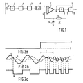
- the brightness signal V had a course before the frequency modulation and recording as shown in Fig. 2a. 2a, the brightness signal V suddenly changes its image content from a black level S to a white level W, ie the frequency of the frequency-modulated signal has a frequency jump from a low to a high frequency. Especially with the band-video head transmission path and the filtering, the amplitude of the frequency-modulated signal suddenly becomes much smaller with such a frequency jump. In the case of an unfavorable phase position, it can now occur that one or more oscillation trains of the frequency-modulated brightness signal have an abnormal course, as is also shown in FIG. 2b, during a period of time intervals Z of the frequency-modulated brightness signal F. The time interval Z begins at a point in time when the modulated brightness signal changes from black to white.
- the threshold value L of the amplitude limiter which is shown in FIG. 2b, has a constant mean input voltage.
- a high frequency of the frequency-modulated brightness signal F corresponds to a white level, while a low frequency corresponds to a black level.
- several oscillation trains do not intersect the threshold value L during the time interval Z.
- the frequency of the frequency-modulated brightness signal F is thereby reduced in the time interval Z. In the picture which is reproduced in a television receiver after demodulation, therefore, no white but black picture content appears, i.e. an inversion phenomenon occurs.
- the output signal of the low pass 6 is fed to a non-inverting input of an amplitude limiter 7.
- the amplitude limiter 7 contains a differential amplifier which receives a differential signal, composed of the difference between the output signal of the low pass 6 and the output signal of a low pass 12. Because of the non-linear circuit properties of the differential amplifier, a limiting effect occurs.
- the output of the amplitude limiter 7 is connected on the one hand to a delay element 8 and on the other hand to one first input 9 of a multiplier 10.
- the output signal of the delay element 8 is fed to a second input 11 of the multiplier 10 and also to the low-pass filter 12, which contains a resistor 13 and a capacitor 14.
- the delay element and the multiplier 10 form a frequency demodulator referred to as a transit time demodulator.
- One connection point of the resistor 13 is connected to the output of the delay element 8 and the other connection point to the inverting input of the amplitude limiter 7 and to the capacitance 14 connected to a reference potential.
- the delay time T of the delay element 8 should be equal to a quarter of the carrier period of the frequency-modulated brightness signal.
- a practical circuit design has shown that the delay time T must be chosen such that: where f . the lower limit frequency of 3.8 MHz and f o is the upper limit frequency of 4.8 MHz of the frequency swing of the carrier-modulated oscillation.
- the cut-off frequency of the low pass 12 is approximately 3 MHz. When choosing the cut-off frequency of the low-pass filter 12, care must be taken that the output signal of the low-pass filter 12 can follow the fluctuations in the mean time value of the output signal of the delay element 8 quickly enough.
- the low pass 12 outputs an output signal G, which is shown in Fig. 2b. If the signals F and G intersect, the output signal of the amplitude limiter 7 changes its polarity. The signal G is therefore the threshold value of the amplitude limiter 7. The threshold value of the amplitude After the signals F and G have intersected, the limiter is readjusted in the direction of the current signal value.
- the output signal H of the amplitude limiter 7 is in F ig. 2c shown.
- the duration of such a square-wave signal in signal H characterizes the frequency of the frequency-modulated signal. The longer such a square wave signal lasts, the lower the frequency of the frequency-modulated signal. Since the duration of the square-wave signals in the time interval Z is much shorter than the other square-wave signals, the frequency jump from a low to a higher frequency is also demodulated. So there can be no inversion.
Landscapes
- Engineering & Computer Science (AREA)
- Multimedia (AREA)
- Signal Processing (AREA)
- Television Signal Processing For Recording (AREA)
- Picture Signal Circuits (AREA)
Priority Applications (1)
| Application Number | Priority Date | Filing Date | Title |
|---|---|---|---|
| AT87200605T ATE91367T1 (de) | 1986-04-11 | 1987-04-01 | Schaltungsanordnung fuer ein bildwiedergabegeraet. |
Applications Claiming Priority (2)
| Application Number | Priority Date | Filing Date | Title |
|---|---|---|---|
| DE3612266 | 1986-04-11 | ||
| DE3612266A DE3612266C1 (de) | 1986-04-11 | 1986-04-11 | Schaltungsanordnung fuer frequenzmodulierte Bildsignale |
Publications (3)
| Publication Number | Publication Date |
|---|---|
| EP0245886A2 true EP0245886A2 (fr) | 1987-11-19 |
| EP0245886A3 EP0245886A3 (en) | 1989-07-26 |
| EP0245886B1 EP0245886B1 (fr) | 1993-07-07 |
Family
ID=6298497
Family Applications (1)
| Application Number | Title | Priority Date | Filing Date |
|---|---|---|---|
| EP87200605A Expired - Lifetime EP0245886B1 (fr) | 1986-04-11 | 1987-04-01 | Circuit pour un dispositif de reproduction d'images |
Country Status (5)
| Country | Link |
|---|---|
| US (1) | US4897608A (fr) |
| EP (1) | EP0245886B1 (fr) |
| JP (1) | JPS62249575A (fr) |
| AT (1) | ATE91367T1 (fr) |
| DE (2) | DE3612266C1 (fr) |
Families Citing this family (4)
| Publication number | Priority date | Publication date | Assignee | Title |
|---|---|---|---|---|
| DE3713225C1 (de) * | 1987-04-18 | 1988-08-11 | Standard Elektrik Lorenz Ag | Videogeraet mit einem Aufzeichnungstraeger |
| JP2701388B2 (ja) * | 1988-12-09 | 1998-01-21 | ソニー株式会社 | Fm復調回路 |
| JP3390272B2 (ja) * | 1994-11-10 | 2003-03-24 | 沖電気工業株式会社 | 同期検波回路 |
| US8677599B2 (en) | 2010-09-20 | 2014-03-25 | Bauer Hockey, Inc. | Blade constructs and methods of forming blade constructs |
Citations (7)
| Publication number | Priority date | Publication date | Assignee | Title |
|---|---|---|---|---|
| FR2237358A1 (en) * | 1973-07-13 | 1975-02-07 | Thomson Brandt | Angularly modulated carrier oscillation demodulator - for video disc reading involves using limiter differential amplifier |
| DE2631335A1 (de) * | 1975-07-14 | 1977-02-03 | Victor Company Of Japan | Schaltungsanordnung zur amplitudenbegrenzung von frequenzmodulierten videosignalen |
| US4142208A (en) * | 1976-07-16 | 1979-02-27 | Thomson-Brandt | System for automatically correcting the duty factor of the carrier wave arising from reading-out a data carrier |
| US4363053A (en) * | 1979-10-23 | 1982-12-07 | Sony Corporation | Signal reproducing circuit |
| DE3223846A1 (de) * | 1981-06-26 | 1983-01-13 | Hitachi, Ltd., Tokyo | Signalwiedergabeschaltung fuer einen bildbandrekorder |
| US4470080A (en) * | 1981-05-14 | 1984-09-04 | Olympus Optical Co. Ltd. | Circuit for detecting frequency modulated signal |
| JPS60216681A (ja) * | 1984-04-12 | 1985-10-30 | Sony Corp | Fm復調回路 |
Family Cites Families (3)
| Publication number | Priority date | Publication date | Assignee | Title |
|---|---|---|---|---|
| JPS5214951B1 (fr) * | 1970-09-22 | 1977-04-25 | ||
| JPS5472659A (en) * | 1977-11-21 | 1979-06-11 | Sony Corp | Fm demodulation circuit |
| US4585952A (en) * | 1982-03-04 | 1986-04-29 | Sansui Electric Co., Ltd. | Digital waveform shaping circuit |
-
1986
- 1986-04-11 DE DE3612266A patent/DE3612266C1/de not_active Expired
-
1987
- 1987-04-01 EP EP87200605A patent/EP0245886B1/fr not_active Expired - Lifetime
- 1987-04-01 AT AT87200605T patent/ATE91367T1/de not_active IP Right Cessation
- 1987-04-01 DE DE8787200605T patent/DE3786420D1/de not_active Expired - Fee Related
- 1987-04-08 JP JP62084884A patent/JPS62249575A/ja active Pending
- 1987-04-09 US US07/036,219 patent/US4897608A/en not_active Expired - Fee Related
Patent Citations (7)
| Publication number | Priority date | Publication date | Assignee | Title |
|---|---|---|---|---|
| FR2237358A1 (en) * | 1973-07-13 | 1975-02-07 | Thomson Brandt | Angularly modulated carrier oscillation demodulator - for video disc reading involves using limiter differential amplifier |
| DE2631335A1 (de) * | 1975-07-14 | 1977-02-03 | Victor Company Of Japan | Schaltungsanordnung zur amplitudenbegrenzung von frequenzmodulierten videosignalen |
| US4142208A (en) * | 1976-07-16 | 1979-02-27 | Thomson-Brandt | System for automatically correcting the duty factor of the carrier wave arising from reading-out a data carrier |
| US4363053A (en) * | 1979-10-23 | 1982-12-07 | Sony Corporation | Signal reproducing circuit |
| US4470080A (en) * | 1981-05-14 | 1984-09-04 | Olympus Optical Co. Ltd. | Circuit for detecting frequency modulated signal |
| DE3223846A1 (de) * | 1981-06-26 | 1983-01-13 | Hitachi, Ltd., Tokyo | Signalwiedergabeschaltung fuer einen bildbandrekorder |
| JPS60216681A (ja) * | 1984-04-12 | 1985-10-30 | Sony Corp | Fm復調回路 |
Non-Patent Citations (1)
| Title |
|---|
| PATENT ABSTRACTS OF JAPAN, Band 10, Nr. 65 (E-388)[2122], 14. März 1986; & JP-A-60 216 681 (SONY K.K.) 30-10-1985 * |
Also Published As
| Publication number | Publication date |
|---|---|
| US4897608A (en) | 1990-01-30 |
| DE3786420D1 (de) | 1993-08-12 |
| EP0245886B1 (fr) | 1993-07-07 |
| EP0245886A3 (en) | 1989-07-26 |
| DE3612266C1 (de) | 1987-06-19 |
| ATE91367T1 (de) | 1993-07-15 |
| JPS62249575A (ja) | 1987-10-30 |
Similar Documents
| Publication | Publication Date | Title |
|---|---|---|
| DE3134737C2 (fr) | ||
| DE3644290A1 (de) | Anordnung zur automatischen verstaerkungsregelung eines verschluesselten videosignals | |
| DE2733350C2 (de) | Schaltungsanordnung zur Beseitigung von Amplitudenschwankungen bei der Wiedergabe eines auf einem Aufzeichnungsträger aufgezeichneten Signals | |
| DE2646214C3 (de) | Anordnung zum Aufzeichnen und/oder zur Wiedergabe von Farbbildsignalgemischen | |
| DE2609555A1 (de) | Einrichtung zum wahrnehmen und kompensieren von fehlern in einem signalumsetzungssystem | |
| DE2655644B2 (de) | Bildplattenspieler | |
| DE2738189C2 (de) | Störunterdrückungsschaltung | |
| DE2822837A1 (de) | Anordnung zur verminderung des stoeranteils in nutzsignalen | |
| DE2551589C3 (de) | Störungskompensationsschaltung | |
| DE2631335C3 (de) | Schaltungsanordnung für frequenzmodulierte Videosignale, die von einem magnetischen Aufzeichnungsträger zur Wiedergabe abgenommen werden | |
| DE3223249C2 (fr) | ||
| EP0245886B1 (fr) | Circuit pour un dispositif de reproduction d'images | |
| DE3014052A1 (de) | Fm-fehlerkompensationsschaltung | |
| DE3117074C2 (fr) | ||
| DE3121600A1 (de) | Videorecorder mit verbesserter aufzeichnung des tonsignals | |
| DE3022781A1 (de) | Farbvideosignal-aufzeichnungs- und wiedergabeeinrichtung | |
| DE2644465C2 (de) | Schaltung zur Überwachung des Pegels von Chrominanzsignalen in Farbbild-Videosignalen unterschiedlichen Standards | |
| DE3201451C2 (de) | "Informationswiedergabevorrichtung" | |
| DE2551588C3 (de) | Abspieleinrichtung für Bildplatten | |
| DE3439898A1 (de) | Vorrichtung zum demodulieren eines frequenzmodulierten eingangssignals | |
| DE3725683C2 (de) | Aufzeichnungsgerät für Videosignale | |
| DE3150754A1 (de) | "schaltungsanordnung zum extrahieren eines pcm-signals aus einem signalgemisch" | |
| EP0208121B1 (fr) | Dispositif pour améliorer la finesse de l'image reproduite dans un enregistreur vidéo | |
| DE2747335C3 (de) | Wiedergabeeinrichtung für Vielkanal-Schallplatten | |
| DE3220607C2 (de) | Schaltungsanordnung zur Aufzeichnung eines Farbvideosignals nach dem SECAM-System |
Legal Events
| Date | Code | Title | Description |
|---|---|---|---|
| PUAI | Public reference made under article 153(3) epc to a published international application that has entered the european phase |
Free format text: ORIGINAL CODE: 0009012 |
|
| AK | Designated contracting states |
Kind code of ref document: A2 Designated state(s): AT DE FR GB |
|
| PUAL | Search report despatched |
Free format text: ORIGINAL CODE: 0009013 |
|
| AK | Designated contracting states |
Kind code of ref document: A3 Designated state(s): AT DE FR GB |
|
| 17P | Request for examination filed |
Effective date: 19900118 |
|
| 17Q | First examination report despatched |
Effective date: 19911128 |
|
| GRAA | (expected) grant |
Free format text: ORIGINAL CODE: 0009210 |
|
| AK | Designated contracting states |
Kind code of ref document: B1 Designated state(s): AT DE FR GB |
|
| REF | Corresponds to: |
Ref document number: 91367 Country of ref document: AT Date of ref document: 19930715 Kind code of ref document: T |
|
| REF | Corresponds to: |
Ref document number: 3786420 Country of ref document: DE Date of ref document: 19930812 |
|
| GBT | Gb: translation of ep patent filed (gb section 77(6)(a)/1977) |
Effective date: 19931008 |
|
| ET | Fr: translation filed | ||
| PG25 | Lapsed in a contracting state [announced via postgrant information from national office to epo] |
Ref country code: AT Effective date: 19940401 |
|
| PLBE | No opposition filed within time limit |
Free format text: ORIGINAL CODE: 0009261 |
|
| STAA | Information on the status of an ep patent application or granted ep patent |
Free format text: STATUS: NO OPPOSITION FILED WITHIN TIME LIMIT |
|
| 26N | No opposition filed | ||
| PGFP | Annual fee paid to national office [announced via postgrant information from national office to epo] |
Ref country code: GB Payment date: 19950331 Year of fee payment: 9 |
|
| PGFP | Annual fee paid to national office [announced via postgrant information from national office to epo] |
Ref country code: FR Payment date: 19950420 Year of fee payment: 9 |
|
| REG | Reference to a national code |
Ref country code: FR Ref legal event code: CD |
|
| PGFP | Annual fee paid to national office [announced via postgrant information from national office to epo] |
Ref country code: DE Payment date: 19950622 Year of fee payment: 9 |
|
| PG25 | Lapsed in a contracting state [announced via postgrant information from national office to epo] |
Ref country code: GB Effective date: 19960401 |
|
| GBPC | Gb: european patent ceased through non-payment of renewal fee |
Effective date: 19960401 |
|
| PG25 | Lapsed in a contracting state [announced via postgrant information from national office to epo] |
Ref country code: FR Effective date: 19961227 |
|
| PG25 | Lapsed in a contracting state [announced via postgrant information from national office to epo] |
Ref country code: DE Effective date: 19970101 |
|
| REG | Reference to a national code |
Ref country code: FR Ref legal event code: ST |