EP0242446A2 - Système de mesure du rapport cyclique d'impulsions de fréquence variable - Google Patents
Système de mesure du rapport cyclique d'impulsions de fréquence variable Download PDFInfo
- Publication number
- EP0242446A2 EP0242446A2 EP86117559A EP86117559A EP0242446A2 EP 0242446 A2 EP0242446 A2 EP 0242446A2 EP 86117559 A EP86117559 A EP 86117559A EP 86117559 A EP86117559 A EP 86117559A EP 0242446 A2 EP0242446 A2 EP 0242446A2
- Authority
- EP
- European Patent Office
- Prior art keywords
- pulses
- input
- frequency
- gate
- pulse
- Prior art date
- Legal status (The legal status is an assumption and is not a legal conclusion. Google has not performed a legal analysis and makes no representation as to the accuracy of the status listed.)
- Granted
Links
Images


Classifications
-
- F—MECHANICAL ENGINEERING; LIGHTING; HEATING; WEAPONS; BLASTING
- F02—COMBUSTION ENGINES; HOT-GAS OR COMBUSTION-PRODUCT ENGINE PLANTS
- F02D—CONTROLLING COMBUSTION ENGINES
- F02D35/00—Controlling engines, dependent on conditions exterior or interior to engines, not otherwise provided for
- F02D35/0007—Controlling engines, dependent on conditions exterior or interior to engines, not otherwise provided for using electrical feedback
-
- F—MECHANICAL ENGINEERING; LIGHTING; HEATING; WEAPONS; BLASTING
- F02—COMBUSTION ENGINES; HOT-GAS OR COMBUSTION-PRODUCT ENGINE PLANTS
- F02D—CONTROLLING COMBUSTION ENGINES
- F02D41/00—Electrical control of supply of combustible mixture or its constituents
- F02D41/30—Controlling fuel injection
- F02D41/32—Controlling fuel injection of the low pressure type
-
- F—MECHANICAL ENGINEERING; LIGHTING; HEATING; WEAPONS; BLASTING
- F02—COMBUSTION ENGINES; HOT-GAS OR COMBUSTION-PRODUCT ENGINE PLANTS
- F02D—CONTROLLING COMBUSTION ENGINES
- F02D41/00—Electrical control of supply of combustible mixture or its constituents
- F02D41/20—Output circuits, e.g. for controlling currents in command coils
- F02D2041/202—Output circuits, e.g. for controlling currents in command coils characterised by the control of the circuit
- F02D2041/2024—Output circuits, e.g. for controlling currents in command coils characterised by the control of the circuit the control switching a load after time-on and time-off pulses
- F02D2041/2027—Control of the current by pulse width modulation or duty cycle control
Definitions
- the invention is based on a system for measuring the pulse duty factor of pulses of variable frequency, in particular in electronically controlled fuel injection systems for internal combustion engines.
- pulse duty factor pulse width / period
- the period is determined using the first counter, while the pulse width is measured using the second counter.
- the quotient of the two measurement results is then formed by an arithmetic operation.
- the object of the invention is to provide a system for measuring the pulse duty factor of pulses of variable frequency, in which a measurement with a required resolution can be carried out with the least possible technical effort within a wide frequency range.
- the system according to the invention is characterized in that clock pulses are derived, the frequency of which corresponds to a predetermined multiple of the frequency of the pulses (input pulses), and that the pulse duty factor is determined by counting the clock pulses during each pulse.
- the system according to the invention has the advantage that the pulse duty factor can be measured in a wide frequency range with the same resolution, with counters and other digital circuits being designed only for the number of digits required for the required resolution.
- the frequency of the clock pulses can be derived by measuring the period of the pulses and forming the reciprocal of the measurement result and multiplying it by a constant that corresponds to the multiple.
- a second development of the invention consists in that a controllable oscillator, a frequency and phase comparison circuit and a frequency divider are provided for deriving the clock pulses. This enables, for example, the use of commercially available modules, in particular a PLL circuit.
- clock pulses are fed to a first input and the input pulses to a second input of an AND gate and that a counter is connected to the output of the AND gate.
- a further embodiment of the invention is characterized in that a D register is connected to the output of the counter, which is clocked with pulses which are derived from the input pulses and fed to the D register via a second OR gate.
- the D register enables a measured value to be available during the entire period of the pulses to be measured.
- the pulse duty factor becomes either 0% or 100%.
- a duty cycle of 0% there are no pulses, but only a DC voltage with a "0" level and with a duty cycle of 100% a DC voltage with a "1" level. In both cases, no period or pulse frequency can be determined.
- a further development of the invention therefore provides that means are provided for determining whether a pulse duty factor of 100% is present and that a predetermined value is output at a pulse duty factor of 100%.
- circuits in accordance with the developments mentioned serve to determine a pulse duty factor of 100%, and that at a pulse duty factor of 0%, the counter remains at 0 anyway due to the lack of input pulses.
- pulse width is determined independently of the pulse frequency and that a duty cycle of 100% is assumed when a limit value is exceeded and that the limit value is derived from the pulse width of a previous pulse.
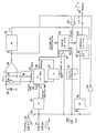
- the exemplary embodiment shown in FIG. 1 is supplied with 1 pulses, the pulse duty factor T1 / T of which is to be measured. So that the system can process pulses of both polarities, a switch 2 and a negation stage are provided at input 1.
- the pulses are first fed to a circuit 4 for measuring the period T. This can be done, for example, by counting pulses with a significantly higher frequency during a period of the input pulses.
- the output signal of the circuit 4 is then fed to an arithmetic circuit 5, which calculates the frequency of the pulses supplied at 1 by reciprocal value formation and multiplies the value obtained by a constant C.
- the constant C is supplied from a corresponding memory 6 to the arithmetic circuit 5.
- the arithmetic circuit 5 At the output of the arithmetic circuit 5 there are pulses whose frequency corresponds to a predetermined multiple of the frequency of the input pulses. The value of the multiple depends on the required resolution of the measurement result.
- the pulses are fed to an input of a triple AND gate 7.
- the input pulses processed in a pulse shaper 8 are fed to a further input of the triple AND gate 7.
- the triple AND gate 7 accordingly causes the clock pulses specified by the circuit 5 to be passed to the n-bit counter 9 only during the occurrence of the input pulses.
- the counter reading reached after a pulse corresponds to the duty cycle because of the coupling of the frequencies of the clock pulses and the input pulses.
- the count result V can then be taken from the output of the n-bit counter 9.
- the n-bit counter 9 is set to 0.
- a corresponding signal is supplied to the n-bit counter by a control block 10.
- the control block has further tasks, which are explained below. Particularly in the case of electronically controlled fuel injection systems, it can happen that the input pulses supplied at 1 either become so wide that they become a continuous voltage (duty cycle 100%) or the injection is switched off completely, so that the duty cycle becomes 0. In this case, the circuits 4 and 5 no longer allow the frequency of the input pulses to be determined, so that no corresponding clock pulses can be derived.
- the circuits 11 and 12 together with the control block 10 already mentioned and a level detector 13 are used to record these operating states.
- the operating states are recorded in the form of a so-called time-out monitoring in dynamic way.
- the frequency and the width of the input pulses change only relatively slowly because of the inertia of the internal combustion engine, while a change in the pulse width occurs suddenly when a duty cycle of 100% is reached.
- the pulse width is first measured in a circuit 11.
- a limit value is formed from this in the circuit 12, which is at most to be expected for the following pulse. This can be done by addition or multiplication.
- the width of the following pulse is compared with this value.
- the control block 10 releases an input register of the n-bit counter 9 provided for the constant C via the line 14, as a result of which the counter reading assumes the value of the constant C.
- the third input of the triple AND gate 7 is set to 0 by the control block 10 via the line 15, so that the counter remains at the value C.
- the pulse duty factor of the input pulses remains at 100%, the input signal is continuously compared with the limit value which was determined from the last individual pulse before the transition to the pulse duty factor of 100%. This enables a termination of the 100% duty cycle to be recognized and the subsequent individual pulse to be checked again as described.
- the level detector 13 In order to achieve a correct result even in the event that the pulse width T1 approaches 0, such a case is determined in the level detector 13.
- the output of the level detector 13 is connected to an input of the control block, from which, in the absence of pulses via a line 16, the n-bit counter 9 is set to 0 and prevents further counting via the line 15 and the triple AND gate 7 becomes. With the level detector 13 it is additionally achieved that the required starting conditions can be created when the system is switched on.
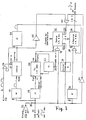
- the system shown in FIG. 2 can in turn be used to process pulses of different polarities, for which purpose an input 21 is directly connected and another input 22 is connected via an inverting amplifier 23 and a switch 24. With a frequency divider 25, pulses with half the frequency and with a duty cycle of 50% are generated from the input pulses. These pulses are fed to a PLL circuit 26.
- the PLL circuit 26 essentially includes a controllable oscillator (VCO) and a frequency and phase comparison circuit.
- the output voltage of the controllable oscillator is fed via a frequency divider 27 to an input of the frequency and phase comparison circuit and is compared there with the pulses supplied by the frequency divider 25.
- a voltage, which represents the result of the comparison, is supplied via an RC element 28, 29 to the control input of the controllable oscillator.
- the described regulation of the controllable oscillator causes the frequency of the oscillator tors assumes a value which is greater by the division ratio of the circuit 27 than the frequency of the pulses which are supplied to the PLL circuit 26.
- the ratio n can be entered at 30 depending on the requirements in individual cases.
- the clock pulses are supplied to the counter 32 via the AND circuit 31.
- the input pulses are fed to a further input of the AND circuit, so that only those clock pulses which occur within a pulse arrive at the counter.
- the count of the counter 32 thus represents a measure of the duty cycle.
- the counter reading is written into a D register 33, which in the exemplary embodiment shown is connected to the counter 32 via 8 lines for 1 bit each.
- the D register 33 is clocked by the input pulses via an OR circuit 35 and a monostable multivibrator 36. This has the effect that after the counting of the clock pulses the count is transferred to the D register.
- a delayed reset pulse is generated by the delay circuit 37, which resets the counter to 0 after data has been transferred from the counter 32 to the D register 33.
- the frequency of the signals which are fed to the PLL circuit 26 reaches the value 0. This can be done by monitoring the output voltage of the frequency and phase comparison circuit of the PLL circuit 26 with the aid of a comparator 38 are found. For this purpose, the one input of the comparator with the control voltage of the controllable Oscillator applied, while a reference voltage is supplied to the other input via a voltage divider 39, 40.
- the output voltage of the comparator 38 assumes the logic value 0, which is fed to an input of the OR gate 41. If the pulse duty factor is 100%, a 0 is present at the other input of the OR gate 41 via the inverter 43. The 0 thus present at the output of the OR gate 41 causes the counter to be set to the value which corresponds to a pulse duty factor of 100% via the inverting preset input of the counter.
- the output voltage of the comparator 38 is also fed to a monostable multivibrator 42, the output signal of which is fed via the OR gate 35 to the clock input of the D register 33.
- the trailing edge of the output signal of the monostable multivibrator 38 causes the count (100%) to be transferred to the D register 33.
- the output of the D register 30 forms the output 34 of the system, from which the measurement result Z can be found.
- a monostable multivibrator 51 generates a pulse of constant width, with which a counter 52 is reset.
- a signal is fed to the counter 52 as a clock via an input 53 provided for this purpose and via an OR gate 54.
- the carry output of the counter 52 is connected to a further input of the OR gate 54, so that no further count pulses reach the counter 52 in the event of a carry.
- the carry signal of the counter 52 is also fed via an inverter 55 to an input of the OR gate 41.
- a monostable multivibrator 56 is connected to the carry output of the counter 52, the output of which is connected to an input of the OR gate 35.
- the counter 52 is set to 0 at the beginning of each period T of the input signal supplied at 21 and then counts the clock pulses supplied at 53, the frequency of which is substantially higher than that of the input pulses.
- the capacity of the counter 52 is now selected such that no carry out takes place within a clock period T of the input pulses. As long as the pulse width T1 has not reached 100%, the counter 52 is set to 0 at the beginning of each clock period T. If, however, 100% duty cycle is reached, the reset is not necessary and after a predetermined number of pulses of the clock signal supplied at 53, a 1 is present at the carry output of the counter 52.
- the counter is stopped, so that the carry remains at the output until a reset pulse comes from the input 21 via the monostable multivibrator 51.
- the input pulses in the system according to FIG. 4 are fed to a circuit 61 for measuring the period duration. This can be done in a manner known per se by counting pulses during a period, the frequency of the counting pulses being substantially greater than the frequency of the input pulses.
- the measured period T is multiplied by a constant stored at 63 or this constant is added to the period.
- Corresponding signals for selection between multiplication and addition can be supplied at the inputs 64 and 65.
- a constant adapted to the respective application can be entered via input 66.
- a value Tmax which corresponds to the period that can be expected as a maximum without a duty cycle of 100% being achieved.
- This value is delayed at 67 by a period T and compared in a comparator 68 with the period of the following period. If the period T (1) is greater than the maximum period Tmax (0) determined from the previous period, the comparison circuit 68 feeds a 0 to the monostable multivibrator 42 and the OR gate 41, which is already the case in connection with FIG 2 triggers the functions described.
Landscapes
- Engineering & Computer Science (AREA)
- Chemical & Material Sciences (AREA)
- Combustion & Propulsion (AREA)
- Mechanical Engineering (AREA)
- General Engineering & Computer Science (AREA)
- Manipulation Of Pulses (AREA)
- Measurement Of Unknown Time Intervals (AREA)
- Measurement Of Mechanical Vibrations Or Ultrasonic Waves (AREA)
Applications Claiming Priority (2)
| Application Number | Priority Date | Filing Date | Title |
|---|---|---|---|
| DE19863611565 DE3611565A1 (de) | 1986-04-07 | 1986-04-07 | System zur messung des tastverhaeltnisses von impulsen veraenderlicher frequenz |
| DE3611565 | 1986-04-07 |
Publications (3)
| Publication Number | Publication Date |
|---|---|
| EP0242446A2 true EP0242446A2 (fr) | 1987-10-28 |
| EP0242446A3 EP0242446A3 (en) | 1988-11-17 |
| EP0242446B1 EP0242446B1 (fr) | 1990-03-07 |
Family
ID=6298089
Family Applications (1)
| Application Number | Title | Priority Date | Filing Date |
|---|---|---|---|
| EP86117559A Revoked EP0242446B1 (fr) | 1986-04-07 | 1986-12-17 | Système de mesure du rapport cyclique d'impulsions de fréquence variable |
Country Status (5)
| Country | Link |
|---|---|
| US (1) | US4841451A (fr) |
| EP (1) | EP0242446B1 (fr) |
| JP (1) | JPS6311870A (fr) |
| BR (1) | BR8701584A (fr) |
| DE (2) | DE3611565A1 (fr) |
Cited By (1)
| Publication number | Priority date | Publication date | Assignee | Title |
|---|---|---|---|---|
| WO1995016118A1 (fr) * | 1993-12-08 | 1995-06-15 | Robert Bosch Gmbh | Procede et dispositif d'excitation d'un consommateur electromagnetique |
Families Citing this family (5)
| Publication number | Priority date | Publication date | Assignee | Title |
|---|---|---|---|---|
| US5249132A (en) * | 1990-10-31 | 1993-09-28 | Tektronix, Inc. | Digital pulse generator |
| US5367200A (en) * | 1993-11-29 | 1994-11-22 | Northern Telecom Limited | Method and apparatus for measuring the duty cycle of a digital signal |
| US5544065A (en) * | 1994-08-09 | 1996-08-06 | Eaton Corporation | Apparatus for digitizing ac signals of unknown or changing frequency |
| DE4429426C2 (de) * | 1994-08-19 | 2002-10-10 | Teves Gmbh Alfred | Frequenzwandler mit konstantem Übersetzungsverhältnis einer veränderbaren Eingangsfrequenz |
| DE50212540D1 (de) | 2001-08-01 | 2008-09-04 | Ebm Papst St Georgen Gmbh & Co | Ür die zeitliche dauer eines sich periodisch wiederholenden impulsförmigen signals, und vorrichtung zur durchführung eines solchen verfahrens |
Citations (2)
| Publication number | Priority date | Publication date | Assignee | Title |
|---|---|---|---|---|
| US4200063A (en) * | 1978-03-20 | 1980-04-29 | General Motors Corporation | Engine fuel injection control apparatus with simultaneous pulse width and frequency adjustment |
| US4554634A (en) * | 1982-04-02 | 1985-11-19 | Toyota Jidosha Kabushiki Kaisha | Electronically controlled fuel injection system |
Family Cites Families (2)
| Publication number | Priority date | Publication date | Assignee | Title |
|---|---|---|---|---|
| JPS5915640A (ja) * | 1982-07-16 | 1984-01-26 | Diesel Kiki Co Ltd | 燃料噴射ポンプ用タイマ装置 |
| US4600994A (en) * | 1982-10-06 | 1986-07-15 | Takeda Riken Kogyo Kabushikikaisha | Phase difference measuring apparatus |
-
1986
- 1986-04-07 DE DE19863611565 patent/DE3611565A1/de not_active Withdrawn
- 1986-12-17 DE DE8686117559T patent/DE3669348D1/de not_active Revoked
- 1986-12-17 EP EP86117559A patent/EP0242446B1/fr not_active Revoked
-
1987
- 1987-04-06 BR BR8701584A patent/BR8701584A/pt unknown
- 1987-04-07 JP JP62083968A patent/JPS6311870A/ja active Pending
- 1987-04-07 US US07/035,556 patent/US4841451A/en not_active Expired - Fee Related
Patent Citations (2)
| Publication number | Priority date | Publication date | Assignee | Title |
|---|---|---|---|---|
| US4200063A (en) * | 1978-03-20 | 1980-04-29 | General Motors Corporation | Engine fuel injection control apparatus with simultaneous pulse width and frequency adjustment |
| US4554634A (en) * | 1982-04-02 | 1985-11-19 | Toyota Jidosha Kabushiki Kaisha | Electronically controlled fuel injection system |
Cited By (2)
| Publication number | Priority date | Publication date | Assignee | Title |
|---|---|---|---|---|
| WO1995016118A1 (fr) * | 1993-12-08 | 1995-06-15 | Robert Bosch Gmbh | Procede et dispositif d'excitation d'un consommateur electromagnetique |
| US5592921A (en) * | 1993-12-08 | 1997-01-14 | Robert Bosch Gmbh | Method and device for actuating an electromagnetic load |
Also Published As
| Publication number | Publication date |
|---|---|
| EP0242446B1 (fr) | 1990-03-07 |
| JPS6311870A (ja) | 1988-01-19 |
| EP0242446A3 (en) | 1988-11-17 |
| DE3611565A1 (de) | 1987-10-08 |
| US4841451A (en) | 1989-06-20 |
| BR8701584A (pt) | 1988-01-26 |
| DE3669348D1 (de) | 1990-04-12 |
Similar Documents
| Publication | Publication Date | Title |
|---|---|---|
| DE2902680C2 (de) | Bandpaßfilterschaltung | |
| DE2643692C2 (de) | Vorrichtung und Verfahren zur schnelleren Zeitbasisfehler-Korrektur | |
| DE2637381C2 (de) | Zeitsteuerungswiedergewinnungsschaltung | |
| DE3816973C2 (fr) | ||
| DE3022307C2 (de) | Zündzeitpunkt-Steuereinrichtung | |
| DE2838549A1 (de) | Impulsbreitenmesschaltung | |
| DE2644823A1 (de) | Kreuzkorrelationsanordnung | |
| DE2427225A1 (de) | Verfahren und schaltungsanordnung zur demodulation digitaler information | |
| DE3332152C2 (fr) | ||
| DE3022746A1 (de) | Digitale phasenkomparatorschaltung | |
| DE2439937C3 (de) | Schaltungsanordnung zur Erzeugung eines gegenüber einem Eingangsimpuls verzögerten Ausgangsimpulses | |
| DE2216123B2 (de) | Verfahren und Anordnung zur Analog-Digital-Umsetzung unter mehrfacher Integration | |
| EP0215810B1 (fr) | Circuit d'obtention d'une valeur moyenne | |
| DE1947792A1 (de) | Vier-Quadranten-Impulsbreiten-Multiplikator | |
| EP1391029B1 (fr) | Procede pour determiner la position angulaire de l'arbre d'entrainement d'un moteur a courant continu a commutation | |
| EP0242446B1 (fr) | Système de mesure du rapport cyclique d'impulsions de fréquence variable | |
| DE3533467C2 (de) | Verfahren und Anordnung zum störsicheren Erkennen von in Datensignalen enthaltenen Daten | |
| DE3834865A1 (de) | Verfahren und schaltung zur ableitung von h- und v-frequenten synchronimpulsen | |
| DE3048673C2 (de) | Frequenz-Diskriminator | |
| DE112019006429T5 (de) | Filter zur Beseitigung von Störungen aus Signalen | |
| DE2532729A1 (de) | Verfahren zur Erfassung der Verschlechterung von Lesesignalen und Anordnung zur Durchfuehrung eines solchen Verfahrens | |
| DE3042267C2 (de) | Schaltungsanordnung zum Regeln der Drehzahl eines mit zwei Drehzahlen zu betreibenden Elektromotors | |
| DE2646367C2 (de) | Detektor von Übergängen eines Signals | |
| DE3843261A1 (de) | Schaltungsanordnung zur steuerung der phase eines taktsignals | |
| DE3832330C2 (de) | Schaltungsanordnung zur Ableitung von horizontalfrequenten und veritikalfrequenten Impulsen |
Legal Events
| Date | Code | Title | Description |
|---|---|---|---|
| PUAI | Public reference made under article 153(3) epc to a published international application that has entered the european phase |
Free format text: ORIGINAL CODE: 0009012 |
|
| AK | Designated contracting states |
Kind code of ref document: A2 Designated state(s): DE FR GB IT |
|
| PUAL | Search report despatched |
Free format text: ORIGINAL CODE: 0009013 |
|
| RHK1 | Main classification (correction) |
Ipc: F02D 41/32 |
|
| AK | Designated contracting states |
Kind code of ref document: A3 Designated state(s): DE FR GB IT |
|
| 17P | Request for examination filed |
Effective date: 19881202 |
|
| 17Q | First examination report despatched |
Effective date: 19890817 |
|
| GRAA | (expected) grant |
Free format text: ORIGINAL CODE: 0009210 |
|
| AK | Designated contracting states |
Kind code of ref document: B1 Designated state(s): DE FR GB IT |
|
| ET | Fr: translation filed | ||
| REF | Corresponds to: |
Ref document number: 3669348 Country of ref document: DE Date of ref document: 19900412 |
|
| GBT | Gb: translation of ep patent filed (gb section 77(6)(a)/1977) | ||
| ITF | It: translation for a ep patent filed |
Owner name: STUDIO JAUMANN |
|
| PGFP | Annual fee paid to national office [announced via postgrant information from national office to epo] |
Ref country code: DE Payment date: 19901123 Year of fee payment: 5 |
|
| PGFP | Annual fee paid to national office [announced via postgrant information from national office to epo] |
Ref country code: GB Payment date: 19901206 Year of fee payment: 5 |
|
| PGFP | Annual fee paid to national office [announced via postgrant information from national office to epo] |
Ref country code: FR Payment date: 19901207 Year of fee payment: 5 |
|
| PLBI | Opposition filed |
Free format text: ORIGINAL CODE: 0009260 |
|
| ITTA | It: last paid annual fee | ||
| 26 | Opposition filed |
Opponent name: ROBERT BOSCH GMBH Effective date: 19901204 |
|
| RDAG | Patent revoked |
Free format text: ORIGINAL CODE: 0009271 |
|
| STAA | Information on the status of an ep patent application or granted ep patent |
Free format text: STATUS: PATENT REVOKED |
|
| 27W | Patent revoked |
Effective date: 19910920 |
|
| GBPR | Gb: patent revoked under art. 102 of the ep convention designating the uk as contracting state |