EP0242207A2 - Verfahren zur Herstellung einer niedergeschlagenen Schicht - Google Patents
Verfahren zur Herstellung einer niedergeschlagenen Schicht Download PDFInfo
- Publication number
- EP0242207A2 EP0242207A2 EP87303341A EP87303341A EP0242207A2 EP 0242207 A2 EP0242207 A2 EP 0242207A2 EP 87303341 A EP87303341 A EP 87303341A EP 87303341 A EP87303341 A EP 87303341A EP 0242207 A2 EP0242207 A2 EP 0242207A2
- Authority
- EP
- European Patent Office
- Prior art keywords
- forming
- deposited film
- film
- substrate
- compound
- Prior art date
- Legal status (The legal status is an assumption and is not a legal conclusion. Google has not performed a legal analysis and makes no representation as to the accuracy of the status listed.)
- Granted
Links
Images
Classifications
-
- C—CHEMISTRY; METALLURGY
- C23—COATING METALLIC MATERIAL; COATING MATERIAL WITH METALLIC MATERIAL; CHEMICAL SURFACE TREATMENT; DIFFUSION TREATMENT OF METALLIC MATERIAL; COATING BY VACUUM EVAPORATION, BY SPUTTERING, BY ION IMPLANTATION OR BY CHEMICAL VAPOUR DEPOSITION, IN GENERAL; INHIBITING CORROSION OF METALLIC MATERIAL OR INCRUSTATION IN GENERAL
- C23C—COATING METALLIC MATERIAL; COATING MATERIAL WITH METALLIC MATERIAL; SURFACE TREATMENT OF METALLIC MATERIAL BY DIFFUSION INTO THE SURFACE, BY CHEMICAL CONVERSION OR SUBSTITUTION; COATING BY VACUUM EVAPORATION, BY SPUTTERING, BY ION IMPLANTATION OR BY CHEMICAL VAPOUR DEPOSITION, IN GENERAL
- C23C16/00—Chemical coating by decomposition of gaseous compounds, without leaving reaction products of surface material in the coating, i.e. chemical vapour deposition [CVD] processes
- C23C16/22—Chemical coating by decomposition of gaseous compounds, without leaving reaction products of surface material in the coating, i.e. chemical vapour deposition [CVD] processes characterised by the deposition of inorganic material, other than metallic material
- C23C16/24—Deposition of silicon only
-
- C—CHEMISTRY; METALLURGY
- C23—COATING METALLIC MATERIAL; COATING MATERIAL WITH METALLIC MATERIAL; CHEMICAL SURFACE TREATMENT; DIFFUSION TREATMENT OF METALLIC MATERIAL; COATING BY VACUUM EVAPORATION, BY SPUTTERING, BY ION IMPLANTATION OR BY CHEMICAL VAPOUR DEPOSITION, IN GENERAL; INHIBITING CORROSION OF METALLIC MATERIAL OR INCRUSTATION IN GENERAL
- C23C—COATING METALLIC MATERIAL; COATING MATERIAL WITH METALLIC MATERIAL; SURFACE TREATMENT OF METALLIC MATERIAL BY DIFFUSION INTO THE SURFACE, BY CHEMICAL CONVERSION OR SUBSTITUTION; COATING BY VACUUM EVAPORATION, BY SPUTTERING, BY ION IMPLANTATION OR BY CHEMICAL VAPOUR DEPOSITION, IN GENERAL
- C23C16/00—Chemical coating by decomposition of gaseous compounds, without leaving reaction products of surface material in the coating, i.e. chemical vapour deposition [CVD] processes
- C23C16/02—Pretreatment of the material to be coated
- C23C16/0227—Pretreatment of the material to be coated by cleaning or etching
- C23C16/0236—Pretreatment of the material to be coated by cleaning or etching by etching with a reactive gas
-
- C—CHEMISTRY; METALLURGY
- C23—COATING METALLIC MATERIAL; COATING MATERIAL WITH METALLIC MATERIAL; CHEMICAL SURFACE TREATMENT; DIFFUSION TREATMENT OF METALLIC MATERIAL; COATING BY VACUUM EVAPORATION, BY SPUTTERING, BY ION IMPLANTATION OR BY CHEMICAL VAPOUR DEPOSITION, IN GENERAL; INHIBITING CORROSION OF METALLIC MATERIAL OR INCRUSTATION IN GENERAL
- C23C—COATING METALLIC MATERIAL; COATING MATERIAL WITH METALLIC MATERIAL; SURFACE TREATMENT OF METALLIC MATERIAL BY DIFFUSION INTO THE SURFACE, BY CHEMICAL CONVERSION OR SUBSTITUTION; COATING BY VACUUM EVAPORATION, BY SPUTTERING, BY ION IMPLANTATION OR BY CHEMICAL VAPOUR DEPOSITION, IN GENERAL
- C23C16/00—Chemical coating by decomposition of gaseous compounds, without leaving reaction products of surface material in the coating, i.e. chemical vapour deposition [CVD] processes
- C23C16/44—Chemical coating by decomposition of gaseous compounds, without leaving reaction products of surface material in the coating, i.e. chemical vapour deposition [CVD] processes characterised by the method of coating
- C23C16/448—Chemical coating by decomposition of gaseous compounds, without leaving reaction products of surface material in the coating, i.e. chemical vapour deposition [CVD] processes characterised by the method of coating characterised by the method used for generating reactive gas streams, e.g. by evaporation or sublimation of precursor materials
- C23C16/452—Chemical coating by decomposition of gaseous compounds, without leaving reaction products of surface material in the coating, i.e. chemical vapour deposition [CVD] processes characterised by the method of coating characterised by the method used for generating reactive gas streams, e.g. by evaporation or sublimation of precursor materials by activating reactive gas streams before their introduction into the reaction chamber, e.g. by ionisation or addition of reactive species
-
- H—ELECTRICITY
- H10—SEMICONDUCTOR DEVICES; ELECTRIC SOLID-STATE DEVICES NOT OTHERWISE PROVIDED FOR
- H10P—GENERIC PROCESSES OR APPARATUS FOR THE MANUFACTURE OR TREATMENT OF DEVICES COVERED BY CLASS H10
- H10P14/00—Formation of materials, e.g. in the shape of layers or pillars
- H10P14/20—Formation of materials, e.g. in the shape of layers or pillars of semiconductor materials
- H10P14/24—Formation of materials, e.g. in the shape of layers or pillars of semiconductor materials using chemical vapour deposition [CVD]
-
- H—ELECTRICITY
- H10—SEMICONDUCTOR DEVICES; ELECTRIC SOLID-STATE DEVICES NOT OTHERWISE PROVIDED FOR
- H10P—GENERIC PROCESSES OR APPARATUS FOR THE MANUFACTURE OR TREATMENT OF DEVICES COVERED BY CLASS H10
- H10P14/00—Formation of materials, e.g. in the shape of layers or pillars
- H10P14/20—Formation of materials, e.g. in the shape of layers or pillars of semiconductor materials
- H10P14/29—Formation of materials, e.g. in the shape of layers or pillars of semiconductor materials characterised by the substrates
- H10P14/2901—Materials
- H10P14/2922—Materials being non-crystalline insulating materials, e.g. glass or polymers
-
- H—ELECTRICITY
- H10—SEMICONDUCTOR DEVICES; ELECTRIC SOLID-STATE DEVICES NOT OTHERWISE PROVIDED FOR
- H10P—GENERIC PROCESSES OR APPARATUS FOR THE MANUFACTURE OR TREATMENT OF DEVICES COVERED BY CLASS H10
- H10P14/00—Formation of materials, e.g. in the shape of layers or pillars
- H10P14/20—Formation of materials, e.g. in the shape of layers or pillars of semiconductor materials
- H10P14/29—Formation of materials, e.g. in the shape of layers or pillars of semiconductor materials characterised by the substrates
- H10P14/2924—Structures
- H10P14/2925—Surface structures
-
- H—ELECTRICITY
- H10—SEMICONDUCTOR DEVICES; ELECTRIC SOLID-STATE DEVICES NOT OTHERWISE PROVIDED FOR
- H10P—GENERIC PROCESSES OR APPARATUS FOR THE MANUFACTURE OR TREATMENT OF DEVICES COVERED BY CLASS H10
- H10P14/00—Formation of materials, e.g. in the shape of layers or pillars
- H10P14/20—Formation of materials, e.g. in the shape of layers or pillars of semiconductor materials
- H10P14/34—Deposited materials, e.g. layers
- H10P14/3402—Deposited materials, e.g. layers characterised by the chemical composition
- H10P14/3404—Deposited materials, e.g. layers characterised by the chemical composition being Group IVA materials
- H10P14/3411—Silicon, silicon germanium or germanium
-
- H—ELECTRICITY
- H10—SEMICONDUCTOR DEVICES; ELECTRIC SOLID-STATE DEVICES NOT OTHERWISE PROVIDED FOR
- H10P—GENERIC PROCESSES OR APPARATUS FOR THE MANUFACTURE OR TREATMENT OF DEVICES COVERED BY CLASS H10
- H10P14/00—Formation of materials, e.g. in the shape of layers or pillars
- H10P14/20—Formation of materials, e.g. in the shape of layers or pillars of semiconductor materials
- H10P14/34—Deposited materials, e.g. layers
- H10P14/3438—Doping during depositing
- H10P14/3441—Conductivity type
- H10P14/3442—N-type
-
- H—ELECTRICITY
- H10—SEMICONDUCTOR DEVICES; ELECTRIC SOLID-STATE DEVICES NOT OTHERWISE PROVIDED FOR
- H10P—GENERIC PROCESSES OR APPARATUS FOR THE MANUFACTURE OR TREATMENT OF DEVICES COVERED BY CLASS H10
- H10P14/00—Formation of materials, e.g. in the shape of layers or pillars
- H10P14/20—Formation of materials, e.g. in the shape of layers or pillars of semiconductor materials
- H10P14/34—Deposited materials, e.g. layers
- H10P14/3438—Doping during depositing
- H10P14/3441—Conductivity type
- H10P14/3444—P-type
-
- Y—GENERAL TAGGING OF NEW TECHNOLOGICAL DEVELOPMENTS; GENERAL TAGGING OF CROSS-SECTIONAL TECHNOLOGIES SPANNING OVER SEVERAL SECTIONS OF THE IPC; TECHNICAL SUBJECTS COVERED BY FORMER USPC CROSS-REFERENCE ART COLLECTIONS [XRACs] AND DIGESTS
- Y10—TECHNICAL SUBJECTS COVERED BY FORMER USPC
- Y10S—TECHNICAL SUBJECTS COVERED BY FORMER USPC CROSS-REFERENCE ART COLLECTIONS [XRACs] AND DIGESTS
- Y10S117/00—Single-crystal, oriented-crystal, and epitaxy growth processes; non-coating apparatus therefor
- Y10S117/903—Dendrite or web or cage technique
- Y10S117/904—Laser beam
-
- Y—GENERAL TAGGING OF NEW TECHNOLOGICAL DEVELOPMENTS; GENERAL TAGGING OF CROSS-SECTIONAL TECHNOLOGIES SPANNING OVER SEVERAL SECTIONS OF THE IPC; TECHNICAL SUBJECTS COVERED BY FORMER USPC CROSS-REFERENCE ART COLLECTIONS [XRACs] AND DIGESTS
- Y10—TECHNICAL SUBJECTS COVERED BY FORMER USPC
- Y10S—TECHNICAL SUBJECTS COVERED BY FORMER USPC CROSS-REFERENCE ART COLLECTIONS [XRACs] AND DIGESTS
- Y10S117/00—Single-crystal, oriented-crystal, and epitaxy growth processes; non-coating apparatus therefor
- Y10S117/905—Electron beam
-
- Y—GENERAL TAGGING OF NEW TECHNOLOGICAL DEVELOPMENTS; GENERAL TAGGING OF CROSS-SECTIONAL TECHNOLOGIES SPANNING OVER SEVERAL SECTIONS OF THE IPC; TECHNICAL SUBJECTS COVERED BY FORMER USPC CROSS-REFERENCE ART COLLECTIONS [XRACs] AND DIGESTS
- Y10—TECHNICAL SUBJECTS COVERED BY FORMER USPC
- Y10S—TECHNICAL SUBJECTS COVERED BY FORMER USPC CROSS-REFERENCE ART COLLECTIONS [XRACs] AND DIGESTS
- Y10S438/00—Semiconductor device manufacturing: process
- Y10S438/913—Diverse treatments performed in unitary chamber
Definitions
- This invention relates to a process suitable for forming a functional deposited film containing silicon, particularly a polycrystalline silicon deposited film for use in semiconductor devices, photosensitive device, line sensors for image input, image pick-up devices, etc.
- a process for forming a polycrystalline or monocrystalline semiconductor layer composed of coarse grains by exposing a polycrystalline or amorphous semiconductor layer on an insulating substrate to an energy beam has been proposed as prior art.
- a polycrystalline or monocrystalline silicon layer composed of coarse grains can be formed by coating a silicon substrate with an insulating film of Si0 2 or SiN, depositing a polycrystalline layer thereon by_CVD in reduced pressure or normal pressure or by plasma CVD, and subjecting the polycrystalline layer to annealing by irradiation of a continuous laser beam or electron beam.
- a polycrystalline layer composed of coarse grains or a monocrystalline layer is formed by forming regular grooves (gratings) on an insulating film surface, depositing a polycrystalline or amorphous silicon layer thereon, and annealing the layer (graphoepitaxial process).
- this process has a poor reproducibility and the crystal face orientation cannot be completely controlled.
- a novel process for, depositing a film free from these problems has been desired.
- the primary object of the present invention is to provide a novel process for forming a polycrystalline silicon deposited film free from the problems of the prior art-processes as described above and not based on the conventional process.
- Another object of the present invention is to solve the said problems and provide a process for forming a deposited film by which a polycrystalline film of good quality and uniform crystal face orientation can be obtained.
- Still another object of the present invention is to provide a process for forming a polycrystalline deposited film, which comprises selectively irradiating a substrate with an energy beam obtained by previously conversing energy such as an electromagnetic wave such as light, microwave, etc., and an electron beam etc. to limit the sites of crystal nucleation on the substrate, and effecting film formation while controlling crystal grain size of polycrystal.
- an energy beam obtained by previously conversing energy such as an electromagnetic wave such as light, microwave, etc., and an electron beam etc.
- Yet another object of the present invention is to provide a process for forming a polycrystalline deposited film which is suitable for enlargement of the area of the film and can easily accomplish improvement of productivity and bulk production of the film, while attempting to improve the characteristics of the film formed, the film forming speed and reproducibility and also to uniformize film quality.
- a process for forming a deposited film comprising the steps of:
- Crystal nucleation regions can be selectively formed on a substrate, for example, i) by locally and spotwise irradiating the substrate with an energy beam of a convergent electromagnetic wave such as light, microwave, etc. or an electron beam, thereby locally forming a deposited film on the substrate, or ii) by locally etching the substrate, thereby making the substrate surface irregular, or iii) by locally and spotwise irradiating the substrate with an energy beam, thereby crystallizing parts of the substrate surface or iv) effecting isomerization treatment of the substrate surface, thereby changing the adsorption characteristics or chemical activity of the substrate surface; that is, providing locally a surface-energetic or physical localization on the substrate.
- a convergent electromagnetic wave such as light, microwave, etc. or an electron beam
- process (i) there is mentioned, for example, a process comprising irradiating a substrate locally and spotwise through reactive gases with an energy beam obtained by converging an electromagnetic wave such as light, microwave, etc. or an electron beam to locally deposit a deposit film onto the substrate.
- an energy beam obtained by converging an electromagnetic wave such as light, microwave, etc. or an electron beam to locally deposit a deposit film onto the substrate.
- process (ii) there is mentioned, for example, a process in which the -substrate surface is locally made irregular by using a reactive etching gas in place of reactive gases, or a process in which a positive type resist is applied to the substrate and the substrate is exposed locally to an energy beam to make the substrate surface irregular.
- a substrate of polymeric material is exposed locally to an energy beam to effect isomerization to form nucleation regions.
- a substrate having a nucleation surface provided selectively on the surface thereof is previously arranged in a film forming space for formation of a deposited film [Step (a)].
- an activated species (A) formed by decomposition of a compound (SX) containing silicon and a halogen and an activated species (B) formed from a chemical substance (B) for film formation which is chemically mutually reactive with the activated species (A) are introduced separately from each other into the film forming space to effect chemical reaction therebetween, thereby forming a deposited film on the substrate [Film forming Step (b)].
- a gaseous substance (E) having etching action on the deposited film to be formed or a gaseous substance (E2) capable of forming the gaseous substance (E) are introduced into the film forming space and the deposited film growth surface is exposed to the gaseous substance (E) to apply etching action on the deposited film growth surface, thereby effecting preferentially crystal growth in a specific face direction [Step (c)].
- the technical advantage accomplished according to the process of the present invention is that the deposited film formed in the copresence of an active species (A) formed by decomposition of a compound containing silicon and halogen and another species (B) formed from a chemical substance for forming a film in a film-forming space in place of generating a plasma is insusceptible to adverse effects of the plasma.
- A active species
- B another species
- Another advantage of the present invention is that a stable CVD process can be provided since the atmosphere temperature of the film forming space and the substrate temperature can be desirably controlled.
- Still another advantage of the present process is accomplished by use of an active species previously activated in a different activation space from the film-forming space. That is the film-forming speed can be made drastically higher and the substrate temperature for forming a deposit film can be made much lower than the conventional CVD process while film characteristic of good quality can be obtained. Furthermore, there can be mentioned the advantage that a crystalline film can be formed having a specific crystal face orientation, that is, a film of good quality with a specific orientation of high degree and uniform grain size by the etching effect of the gaseous material (E) having etching action.
- the compound (SX) containing silicon and halogen to be introduced into the activation space (A) in the present invention includes for example, linear or cyclic silane compounds, part or whole of whose hydrogen atoms are substituted with halogen atoms, are used.
- gaseous or reading gasifying compounds such as SiF 4 , (SiF 2 ) 5 , ( SiF 2 ) 6 , (SiF2)4, Si 2 F 6 , Si 3 F 8 , SiHF 3 , SiH 2 F 2 , SiCl 4 , (SiCl 2 ) 5 , SiBr 4 , ( Si Br 2 ) 5 , Si 2 Cl 6 , Si 2 Br 6 , SiHCl 3 , SiH 3 Cl, SiH 2 Cl 2 , SiHBr 3 , SiHCl 3 , Si 2 Cl 3 F 3 , etc.
- SiF 4 SiF 4 , (SiF 2 ) 5 , ( SiF 2 ) 6 , (SiF2)4, Si 2 F 6 , Si 3 F 8 , SiHF 3 , SiH 2 F 2 , SiCl 4 , (SiCl 2 ) 5 , SiBr 4 , ( Si Br 2 ) 5 , Si 2 Cl 6 , Si 2 Br 6 , SiHCl
- silicon simple substance and other silicon compounds hydrogen, halogen compounds (for example, F 2 gas, C1 2 gas, gasified Br 2 ,I 2 , e t c .), etc. can be used together, if necessary, in addition to the compound containing silicon and halogen (SX).
- halogen compounds for example, F 2 gas, C1 2 gas, gasified Br 2 ,I 2 , e t c .
- the active species (A) is formed in the activation space (A) by an activation energy such as an electric energy, for example, microwave, RF, low frequency wave, DC, etc., a thermal energy such as heater heating, infrared heating, etc., a photo energy, etc. in view of various given conditions and apparatuses.
- an activation energy such as an electric energy, for example, microwave, RF, low frequency wave, DC, etc.
- a thermal energy such as heater heating, infrared heating, etc.
- a photo energy etc. in view of various given conditions and apparatuses.
- the chemical substance for forming a film to form the active species (B) in the activation space (B) hydrogen gas and/or a halogen compound (for example, F 2 gas, Cl 2 gas, gasified Br 2 ,I 2 , etc.) can be advantageously used.
- a halogen compound for example, F 2 gas, Cl 2 gas, gasified Br 2 ,I 2 , etc.
- an inert gas such as helium, argon, neon, etc. can be used.
- these chemical substances for forming a film can be introduced in a gaseous state into the activation space (B) after mixing them in advance, or these chemical substances for forming a film can be separately introduced into the activation space (B) from their independent supply sources, or introduced into the respective, independent activation spaces to make individual activations.
- a mixing ratio of the active species (A) to the active species (B) to be introduced into the film forming space is determined, as desired, in view of the film-forming conditions, kinds of the active species, etc., and is preferably 10:1 to 1:10 (introducing flow rate ratio), more preferably 8:2 to 4:6.
- the deposited film formed according to the present invention can be doped with the so-called impurity element used in the field of semiconductor during or after film formation.
- the impurity element to be used there may be employed, as p-type impurity, an element belonging to the group IIIA of the periodic table such as B, Al, Ga, In, Tl, etc. and, as n-type purity, an element belonging to the group VA of the periodic table such as P, As, Sb, Bi,etc. as suitable ones. Particularly, B, Ga, P and Sb are most preferred.
- the amount of the impurity to be doped may be determined suitably depending on the desired electrical and optical characteristics.
- the substance containing such an impurity atom as the component is preferably to select a compound which is gaseous under normal temperature and normal pressure, or gaseous at least under the activation conditions film and can be readily gasified by a suitable gasifying device.
- Such compounds may include PH 3 ,P 2 H 4 , PF 3 , PF 5 , PCl 3 , AsH 3 , AsF 3 , AsF 5 , AsCl 3 , SbH 3 , SbF 5 , SiH 3 , BF 3 , BCl 3 , BBr 3 ,B 2 H 6 , B 4 H 10 , B 5 H 9 , B 5 H 11 , B 6 H 10 , B6H12' AlCl 3 , etc.
- the compounds containing impurity element may be used either singly or as a combination of two or more compounds.
- the compound containing impurities as element may be directly introduced under gaseous state into the film forming space, or alternatively activated previously in the activation space (A) or the activation space (B) or a third activation space (C) before introduction into the film forming space.
- etching action is applied on the growth surface of the deposited film at the same time, or ( B ) etching action is applied on the growth surface of the deposited film with film formation intermitted, whereby crystal growth can be effected preferentially in a specific face direction to give a deposited film with good crystallinity.
- the etching action in the case of the above ( B ) may be effected within the film forming space or alternatively in an etching space separate from the film forming space.
- gaseous or readily gasifiable substance for etching (E) having etching action on the deposited film containing silicon there may be included single substances of halogen, halogen compounds or activated species (C) formed from these.
- These substances (E) for etching may be introduced under gaseous state into the space where etching action is applied to the deposited film, or alternatively in the case where the substance (E) is formed by the surface reaction on the surface of the deposited film of the above activated species (A) or the above activated species (B), or formed from the chemical reaction between the activated species (A) and the activated species (B), etching action is applied on the growth surface of the deposited film simultaneously with film formation.
- the reaction between an activated species of halogen and hydrogen or a halogen and activated species of hydrogen occurs on the growth surface of the deposited film, and hydrogen halide (HX) is released from the growth surface of the deposited film and the hydrogen halide becomes the substance (E) for etching:
- halogens such as F 2 , Cl 2 , gasified Br 2 , 2, etc., halogenated carbon such as CHF 3 , CF 4 , C 2 F 6 , CCl 4 , C BrF 3 , CCl 2 F 2 , C C1 3 F, CClF 3 , C 2 Cl 2 F 4 , etc., halides including typically boron halides such as BC1 3 , BF 3 and SF 6 , NF 3 , PF s , etc., and further radicals such as F * , Cl * , ions such as CF 3 + , CCl 3 + , from these gases.
- halogens such as F 2 , Cl 2 , gasified Br 2 , 2, etc.
- halogenated carbon such as CHF 3 , CF 4 , C 2 F 6 , CCl 4 , C BrF 3 , CCl 2 F 2 , C C1 3 F, CClF 3 , C 2 Cl 2
- etching and film formation may be repeated alternately by providing separately an etching space, or they can be introduced under the state having etching activity into the film forming space to effect etching action simultaneously with film formation, thereby giving the effect of limiting the growing direction of the crystalline film to accomplish the object of the present invention.
- the dependency of growth r speed upon face direction has been found during crystal growth of silicon or silicon-containing materials. This may differ depending on the deposited film forming method or deposition conditions, but in the method of the present invention, the preferential order has been found to be (110) > (111) > (100).
- the condition with stronger orientability of (110) » (111) » (100) can be realized. It is realized in the present invention to strengthen the above orientability and accelerate the growth speed, particularly by setting a portion for accelerating nucleation on the substrate. And, not only formation of polycrystalline deposited film with great grain size oriented only toward the (110) face is possible, but it is also possible to grow a single crystal by selecting the size, shape, interval, material, etc., of the nucleus.
- the expression crystalline deposited film of course represents a polycrystalline and a single crystal film.
- the nucleation surface provided on the substrate surface in the present invention are provided scatteringly in large number.
- the active species (A) in the vicinity of the substrate formed from compounds containing silicon and a halogen has a great coefficient of attachment.
- a material having a large coefficient of attachment may be employed or a surface structure for enhancing the coefficient of attachment may be formed.
- Coefficient of attachment generally refers to a quantity which is a measure for readiness in chemical adsorption to occur, and in the case of the present invention, physical adsorption and chemical adsorption including dissociation are also included.
- the surface structure enhancing the coefficient of attachment those with surface unevenness of some 0 1000 A or less are preferred.
- the shape those with shapes as regular as possible rather than random are preferred.
- the material having a large coefficient of attachment may be selected from among insulating substances and semiconductive substances such as Si : N : H, Si 3 N 4 , A-Si : H, Si : N : 0 : H, Al 2 O 3 , Si0 2 , Ta 2 0 5 , etc., but particularly a compound containing 3i-N is preferred. Also, a metal material may be sometimes employed. As mentioned above, the order of stronger orientability of crystal has been made as (110) > (111) > (100), but of course it is possible in the present invention to control the direction of oriented surface and the direction of the crystal growth face depending on the conditions of deposition and nucleation.
- the nucleation surface of the present invention does not have to be uniformly spread continuously over the whole substrate surface, but a film with regular sized crystal grains and regular crystal axis directions may be obtained by locally providing the nucleation surface scatteringly while determining its area depending on the purposes.
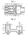
- Fig. 1 is a schematic sectional view illustrating the main part of an apparatus for forming a deposited film for embodying the present process.
- numeral 101 is a deposition compartment where deposition of a silicon thin film is effected, and the deposition compartment 101 is connected to an exhausting system, not shown on the drawing, through a vent 106 to maintain the deposition compartment under a desired pressure.
- an inlet pipe 102 for introducing a radical 107 containing Si and halogen as an activated speices (A), an inlet pipe 103 for introducing a hydrogen radical 107A as an activated species (B) and an inlet pipe 111 for introducing F 2 gas 112 as a gaseous substance (E) having etching action are enlarged to form action compartments 108, 108A and 113, respectively, and are narrowed at the outlet ends 109, 109A and 114, respectively.
- a substrate support 104 is supported by rollers 110 and 110A so that the substrate support 104 can reciprocatingly moved in a direction perpendicular to the drawing surface, and the substrate 105 for deposition on which nucleation surface has been previously provided is supported on the substrate support 104.
- the respective radicals and F 2 gas discharged at the outlet ends 109, 109A and 114 are mixed together near the substrate in the deposition compartment 101 to undergo reaction therebetween and form a deposited film on the substrate 105 while being etched.
- the radicals containing silicon and halogen and the hydrogen radicals are formed from their starting material gases in heating furnaces or radical-forming sections in plasma chambers, etc., not shown in the drawing, respectively, and then introduced into the action compartments 108 and 108A through the inlet pipes 102 and 103, respectively.
- the flow rates of the radicals are controlled by mass flow controllers provided at positions towards the gas sources from the heating furnaces or plasma chambers, respectively.
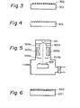
- a glass substrate 205 was placed on a structure holder in a structure pretreatment compartment 214, and exposed through a quartz window 215 to ArF excimer laser having a wavelength of 193 nm and a pulse width of 20 n sec after focussed to a laser spot having a spot size of about 10 pm through an optical system at 8W /cm 2 and 80 pulses, while keeping the glass substrate 205 at 250 °C, and passing 50 sccm of Si 2 H 6 under a pressure of 5 Torr as a reactive gas, whereby amorphous silicon films area 302 where formed at distances of 1 pm (Fig. 3) on the glass state 205.
- the glass substrate 205 is shown as 301 in Fig. 3.
- the substrate 205A whose nucleation formation surface was thus prepared scatteringly on the surface in advance was transferred into a reaction compartment 213 form the nucleation compartment 214 to form a polycrystalline film on the said substrate 205A as follows.
- SiF 4 gas as a raw material gas for forming radicals containing silicon and halogen was introduced into a reaction furnace kept at 1,100 °C, and decomposed, and then discharged into a reaction compartment 208 from an inlet pipe 202, while H 2 gas was introduced into an inlet pipe 203.
- decomposed by supplying a microwave of 2.45 GHz at a power of 0.8 W/cm 2 to the inlet pipe 203 to form hydrogen radical and the said radicals were discharged into the reaction compartment 208.
- XeF 2 as an etching gas was supplied towards the substrate 205A from an inlet pipe 211 at the same time. The substrate was kept at a temperature of 300 °C.
- a ratio of flow rate (sccm) of XeF 2 gas to flow rate (sccm) of SiF 4 was changed to 5/100, 10/100, 15/100, 20/100, and 30/100, each kept under a pressure of 0.5 Torr for one hour to form films.
- films having the characterisitcs shown in Table 1 were deposited. Grain sizes were measured by a transmission type electron microscope.
- the mobility values of sample No. 3 having the best mobility measurement values is shown in Table 2.
- measurement values of sample R in which the polycrystalline Si film formed on a glass substrate having no treatment of formation of nucleation surface as sample No. 3 is shown in Table 2. It is evident from Table 2 that the present invention can provide films of good characteristics, i.e. good orientation and less fluctuation.
- Example 4 A polycrystalline Si film was deposited thereon at the same condition as in sample No. 3 in Example 1 and the characteristics were evaluated in the same manner as in Example 1 (sample 4-1). The results are shown in Tables 2 and 3.
- Example 5 Except reactive etching gas F 2 was used for forming nucleation surface to etch a glass substrate spotwise under a pressure of 5 Torr , the substrate 401 for formation of deposited film having the structure such as shown in Fig. 4 is formed. Using this substrate 401, the polycrystalline Si film was deposited and the characteristics thereof were evaluated in the same manner as Example 1 (Sample 5-1). The results are shown in Tables 2 and 3.
- a glass plate 505 (#7059, made by Corning Glass Works) prebacked after spinner coating of polymethyl methacrylate (P-MMA) as a positive type resist was placed in an electron beam irradiation apparatus as shown in Fig. 5, and then subjected to electron beam irradiation on the resist film as follows. Electrons emitted from an electron gun 501 were irradiated on the glass substrate. As an accelerated convergent electron beam through deflection electrodes 503a and 503b and control electrodes 502a and 502b. The electron beam at this time had 3 mA of a beam current at 5 KeV of an acceleration voltage.
- P-MMA polymethyl methacrylate
- the electron beam was irradiated on the resist film of above-mentioned glass substrate 505 spotwise having a diameter of 0.1 ⁇ m at intervals of 0.1 ⁇ m. There were 10 Torr of vacuum at this time.
- the substrate having a structure as shown in Fig. 6 for forming the deposited film (the glass substrate 505 is shown as 601 and the resist film prepared unevenness on the surface is shown as 602) was prepared.
- the polycrystalline film was deposited on this substrate at the same condition as Sample No. 3 in Example 1 (sample 5-1). About this sample, the characteristics were evaluated in the same manner as Example 1. The results are shown in Tables 2 and 3.
- An oxyphous silicon thin film was formed on a glass substrate by RF glow discharge. Except setting the laser pulse number for 150 and without using the reactive glass, local annealing was done by irradiating the laser on this amorphous silicon thin film on the glass substrate in the same manner as in Example 1, being crystallized locally. Then, a polycrystalline film was deposited on the thus obtained substrate for formation of the deposited film under the same conditions as in Sample No. 3 (sample 7-1). Characteristics of the sample was obtained in the same manner as in Example 1. The results are shown in Tables 2 and 3.
- a film consisting of 11 diacetylene layers was deposited on a glass substrate (#7059, made by corning Glass Works) according to LB method in the following manner. That is, a glass substrate was at first washed with ultrapure water to remove oily matters therefrom, and then dipped into water. Then, a few drops of a solution of diacetylene in chloroform at a concentration of 5 x 10 -3 mol/l was added thereto, and after a given pressure was applied to the liquid surface. Then, the glass substrate was vertically reciprocated at a speed of 1 cm/min while maintaining the pressure to deposit a film consisting of 11 layers. Then, the film was exposed to a focussed UV light (254 nm) at a power of 10 mW/cm 2 to effect local polymerization. So, characteristics for formation of deposited film formed.
Landscapes
- Chemical & Material Sciences (AREA)
- Mechanical Engineering (AREA)
- General Chemical & Material Sciences (AREA)
- Chemical Kinetics & Catalysis (AREA)
- Engineering & Computer Science (AREA)
- Materials Engineering (AREA)
- Metallurgy (AREA)
- Organic Chemistry (AREA)
- Inorganic Chemistry (AREA)
- Chemical Vapour Deposition (AREA)
- Crystals, And After-Treatments Of Crystals (AREA)
- Inorganic Compounds Of Heavy Metals (AREA)
- Superconductors And Manufacturing Methods Therefor (AREA)
Priority Applications (1)
| Application Number | Priority Date | Filing Date | Title |
|---|---|---|---|
| AT87303341T ATE86794T1 (de) | 1986-04-15 | 1987-04-15 | Verfahren zur herstellung einer niedergeschlagenen schicht. |
Applications Claiming Priority (2)
| Application Number | Priority Date | Filing Date | Title |
|---|---|---|---|
| JP86826/86 | 1986-04-15 | ||
| JP61086826A JPH0639703B2 (ja) | 1986-04-15 | 1986-04-15 | 堆積膜形成法 |
Publications (3)
| Publication Number | Publication Date |
|---|---|
| EP0242207A2 true EP0242207A2 (de) | 1987-10-21 |
| EP0242207A3 EP0242207A3 (en) | 1988-09-07 |
| EP0242207B1 EP0242207B1 (de) | 1993-03-10 |
Family
ID=13897615
Family Applications (1)
| Application Number | Title | Priority Date | Filing Date |
|---|---|---|---|
| EP87303341A Expired - Lifetime EP0242207B1 (de) | 1986-04-15 | 1987-04-15 | Verfahren zur Herstellung einer niedergeschlagenen Schicht |
Country Status (8)
| Country | Link |
|---|---|
| US (1) | US4942058A (de) |
| EP (1) | EP0242207B1 (de) |
| JP (1) | JPH0639703B2 (de) |
| AT (1) | ATE86794T1 (de) |
| AU (1) | AU598247B2 (de) |
| CA (1) | CA1292662C (de) |
| DE (1) | DE3784541T2 (de) |
| ES (1) | ES2054666T3 (de) |
Cited By (5)
| Publication number | Priority date | Publication date | Assignee | Title |
|---|---|---|---|---|
| EP0335313A3 (de) * | 1988-03-28 | 1991-03-06 | Kabushiki Kaisha Toshiba | Verfahren zur Herstellung eines Halbleiterbauelementes und hierzu verwendeter Apparat |
| EP0241317B1 (de) * | 1986-04-11 | 1993-03-10 | Canon Kabushiki Kaisha | Herstellungsverfahren einer niedergeschlagenen Schicht |
| EP0243074B1 (de) * | 1986-04-14 | 1993-03-10 | Canon Kabushiki Kaisha | Herstellungsverfahren einer niedergeschlagenen Schicht |
| EP0241311B1 (de) * | 1986-04-11 | 1993-03-17 | Canon Kabushiki Kaisha | Verfahren zur Herstellung einer niedergeschlagenen Schicht |
| EP0242182B1 (de) * | 1986-04-14 | 1993-06-30 | Canon Kabushiki Kaisha | Verfahren zur Herstellung einer niedergeschlagenen Schicht |
Families Citing this family (12)
| Publication number | Priority date | Publication date | Assignee | Title |
|---|---|---|---|---|
| JPH0244786A (ja) * | 1988-08-05 | 1990-02-14 | Canon Inc | ジョセフソン素子の製造方法 |
| JPH02225399A (ja) * | 1988-11-11 | 1990-09-07 | Fujitsu Ltd | エピタキシャル成長方法および成長装置 |
| JPH02208293A (ja) * | 1989-02-08 | 1990-08-17 | Kanazawa Univ | 多結晶シリコン膜の製造方法 |
| JPH02258689A (ja) * | 1989-03-31 | 1990-10-19 | Canon Inc | 結晶質薄膜の形成方法 |
| JP3535241B2 (ja) * | 1994-11-18 | 2004-06-07 | 株式会社半導体エネルギー研究所 | 半導体デバイス及びその作製方法 |
| JP3469337B2 (ja) | 1994-12-16 | 2003-11-25 | 株式会社半導体エネルギー研究所 | 半導体装置の作製方法 |
| US6652922B1 (en) * | 1995-06-15 | 2003-11-25 | Alliedsignal Inc. | Electron-beam processed films for microelectronics structures |
| US6027960A (en) | 1995-10-25 | 2000-02-22 | Semiconductor Energy Laboratory Co., Ltd. | Laser annealing method and laser annealing device |
| US6783627B1 (en) * | 2000-01-20 | 2004-08-31 | Kokusai Semiconductor Equipment Corporation | Reactor with remote plasma system and method of processing a semiconductor substrate |
| US6521961B1 (en) * | 2000-04-28 | 2003-02-18 | Motorola, Inc. | Semiconductor device using a barrier layer between the gate electrode and substrate and method therefor |
| US7087504B2 (en) * | 2001-05-18 | 2006-08-08 | Semiconductor Energy Laboratory Co., Ltd. | Method of manufacturing a semiconductor device by irradiating with a laser beam |
| US6780786B2 (en) * | 2001-11-26 | 2004-08-24 | The Regents Of The University Of California | Method for producing a porous silicon film |
Family Cites Families (13)
| Publication number | Priority date | Publication date | Assignee | Title |
|---|---|---|---|---|
| DE2151346C3 (de) * | 1971-10-15 | 1981-04-09 | Deutsche Itt Industries Gmbh, 7800 Freiburg | Verfahren zum Herstellung einer aus Einkristallschichtteilen und Polykristallschichtteilen bestehenden Halbleiterschicht auf einem Einkristallkörper |
| JPS5587425A (en) * | 1978-12-26 | 1980-07-02 | Tohoku Metal Ind Ltd | Doping method for epitaxial layer of semiconductor |
| JPS5767938A (en) * | 1980-10-16 | 1982-04-24 | Canon Inc | Production of photoconductive member |
| DE3107260A1 (de) * | 1981-02-26 | 1982-09-09 | Siemens AG, 1000 Berlin und 8000 München | Verfahren und vorrichtung zum abscheiden von halbleitermaterial, insbesondere silicium |
| WO1983004269A1 (en) * | 1982-06-01 | 1983-12-08 | Massachusetts Institute Of Technology | Maskless growth of patterned films |
| US4522662A (en) * | 1983-08-12 | 1985-06-11 | Hewlett-Packard Company | CVD lateral epitaxial growth of silicon over insulators |
| JPS6126774A (ja) * | 1984-07-16 | 1986-02-06 | Canon Inc | 非晶質シリコン膜形成装置 |
| FR2580673B1 (fr) * | 1985-04-19 | 1987-09-25 | Haond Michel | Procede de fabrication sur un support isolant d'un film de silicium monocristallin oriente et a defauts localises |
| US4791071A (en) * | 1986-02-20 | 1988-12-13 | Texas Instruments Incorporated | Dual dielectric gate system comprising silicon dioxide and amorphous silicon |
| AU606053B2 (en) * | 1986-04-11 | 1991-01-31 | Canon Kabushiki Kaisha | Process for forming deposited film |
| DE3784537T2 (de) * | 1986-04-11 | 1993-09-30 | Canon Kk | Herstellungsverfahren einer niedergeschlagenen Schicht. |
| JPH0639702B2 (ja) * | 1986-04-14 | 1994-05-25 | キヤノン株式会社 | 堆積膜形成法 |
| EP0242182B1 (de) * | 1986-04-14 | 1993-06-30 | Canon Kabushiki Kaisha | Verfahren zur Herstellung einer niedergeschlagenen Schicht |
-
1986
- 1986-04-15 JP JP61086826A patent/JPH0639703B2/ja not_active Expired - Lifetime
-
1987
- 1987-04-14 AU AU71515/87A patent/AU598247B2/en not_active Ceased
- 1987-04-15 AT AT87303341T patent/ATE86794T1/de active
- 1987-04-15 CA CA000534808A patent/CA1292662C/en not_active Expired - Lifetime
- 1987-04-15 ES ES87303341T patent/ES2054666T3/es not_active Expired - Lifetime
- 1987-04-15 DE DE87303341T patent/DE3784541T2/de not_active Expired - Fee Related
- 1987-04-15 EP EP87303341A patent/EP0242207B1/de not_active Expired - Lifetime
-
1989
- 1989-06-08 US US07/363,309 patent/US4942058A/en not_active Expired - Lifetime
Cited By (6)
| Publication number | Priority date | Publication date | Assignee | Title |
|---|---|---|---|---|
| EP0241317B1 (de) * | 1986-04-11 | 1993-03-10 | Canon Kabushiki Kaisha | Herstellungsverfahren einer niedergeschlagenen Schicht |
| EP0241311B1 (de) * | 1986-04-11 | 1993-03-17 | Canon Kabushiki Kaisha | Verfahren zur Herstellung einer niedergeschlagenen Schicht |
| EP0243074B1 (de) * | 1986-04-14 | 1993-03-10 | Canon Kabushiki Kaisha | Herstellungsverfahren einer niedergeschlagenen Schicht |
| EP0242182B1 (de) * | 1986-04-14 | 1993-06-30 | Canon Kabushiki Kaisha | Verfahren zur Herstellung einer niedergeschlagenen Schicht |
| EP0335313A3 (de) * | 1988-03-28 | 1991-03-06 | Kabushiki Kaisha Toshiba | Verfahren zur Herstellung eines Halbleiterbauelementes und hierzu verwendeter Apparat |
| US5067437A (en) * | 1988-03-28 | 1991-11-26 | Kabushiki Kaisha Toshiba | Apparatus for coating of silicon semiconductor surface |
Also Published As
| Publication number | Publication date |
|---|---|
| ATE86794T1 (de) | 1993-03-15 |
| EP0242207A3 (en) | 1988-09-07 |
| AU7151587A (en) | 1987-10-22 |
| DE3784541T2 (de) | 1993-09-30 |
| DE3784541D1 (de) | 1993-04-15 |
| CA1292662C (en) | 1991-12-03 |
| EP0242207B1 (de) | 1993-03-10 |
| AU598247B2 (en) | 1990-06-21 |
| JPS62243768A (ja) | 1987-10-24 |
| US4942058A (en) | 1990-07-17 |
| JPH0639703B2 (ja) | 1994-05-25 |
| ES2054666T3 (es) | 1994-08-16 |
Similar Documents
| Publication | Publication Date | Title |
|---|---|---|
| US4942058A (en) | Process for forming deposited film | |
| US5246886A (en) | Process for depositing a silicon-containing polycrystalline film on a substrate by way of growing Ge-crystalline nucleus | |
| US5192717A (en) | Process for the formation of a polycrystalline semiconductor film by microwave plasma chemical vapor deposition method | |
| US4918028A (en) | Process for photo-assisted epitaxial growth using remote plasma with in-situ etching | |
| EP0241317B1 (de) | Herstellungsverfahren einer niedergeschlagenen Schicht | |
| US4800173A (en) | Process for preparing Si or Ge epitaxial film using fluorine oxidant | |
| US5294285A (en) | Process for the production of functional crystalline film | |
| US5126169A (en) | Process for forming a deposited film from two mutually reactive active species | |
| US5135607A (en) | Process for forming deposited film | |
| US5439844A (en) | Process for forming deposited film | |
| EP0243074B1 (de) | Herstellungsverfahren einer niedergeschlagenen Schicht | |
| EP0241311B1 (de) | Verfahren zur Herstellung einer niedergeschlagenen Schicht | |
| EP0240306B1 (de) | Verfahren zur Bildung eines abgeschiedenen Filmes | |
| EP0241316B1 (de) | Verfahren zur Herstellung einer niedergeschlagenen kristalliner Schicht | |
| JP2914992B2 (ja) | 堆積膜形成方法 | |
| JP2692803B2 (ja) | 堆積膜形成法 | |
| EP0240305B1 (de) | Herstellungsverfahren einer niedergeschlagenen Schicht | |
| KR20010103984A (ko) | 전이금속박막형상 제어에 의한 탄소나노튜브의 수직 성장방법 | |
| JPH0682616B2 (ja) | 堆積膜形成方法 | |
| JP2649221B2 (ja) | 堆積膜形成法 | |
| US5476694A (en) | Method for forming deposited film by separately introducing an active species and a silicon compound into a film-forming chamber | |
| JP2547741B2 (ja) | 堆積膜製造装置 | |
| JPS62243767A (ja) | 堆積膜形成法 | |
| JPH11214311A (ja) | シリコン膜の形成方法及び太陽電池の製造方法 | |
| JPS62243766A (ja) | 堆積膜形成法 |
Legal Events
| Date | Code | Title | Description |
|---|---|---|---|
| PUAI | Public reference made under article 153(3) epc to a published international application that has entered the european phase |
Free format text: ORIGINAL CODE: 0009012 |
|
| AK | Designated contracting states |
Kind code of ref document: A2 Designated state(s): AT BE CH DE ES FR GB GR IT LI LU NL SE |
|
| PUAL | Search report despatched |
Free format text: ORIGINAL CODE: 0009013 |
|
| AK | Designated contracting states |
Kind code of ref document: A3 Designated state(s): AT BE CH DE ES FR GB GR IT LI LU NL SE |
|
| 17P | Request for examination filed |
Effective date: 19890120 |
|
| 17Q | First examination report despatched |
Effective date: 19900817 |
|
| GRAA | (expected) grant |
Free format text: ORIGINAL CODE: 0009210 |
|
| AK | Designated contracting states |
Kind code of ref document: B1 Designated state(s): AT BE CH DE ES FR GB GR IT LI LU NL SE |
|
| PG25 | Lapsed in a contracting state [announced via postgrant information from national office to epo] |
Ref country code: GR Free format text: LAPSE BECAUSE OF FAILURE TO SUBMIT A TRANSLATION OF THE DESCRIPTION OR TO PAY THE FEE WITHIN THE PRESCRIBED TIME-LIMIT Effective date: 19930310 Ref country code: BE Effective date: 19930310 Ref country code: AT Effective date: 19930310 |
|
| REF | Corresponds to: |
Ref document number: 86794 Country of ref document: AT Date of ref document: 19930315 Kind code of ref document: T |
|
| REF | Corresponds to: |
Ref document number: 3784541 Country of ref document: DE Date of ref document: 19930415 |
|
| PG25 | Lapsed in a contracting state [announced via postgrant information from national office to epo] |
Ref country code: LU Free format text: LAPSE BECAUSE OF NON-PAYMENT OF DUE FEES Effective date: 19930430 |
|
| ET | Fr: translation filed | ||
| ITF | It: translation for a ep patent filed | ||
| PLBE | No opposition filed within time limit |
Free format text: ORIGINAL CODE: 0009261 |
|
| STAA | Information on the status of an ep patent application or granted ep patent |
Free format text: STATUS: NO OPPOSITION FILED WITHIN TIME LIMIT |
|
| 26N | No opposition filed | ||
| ITTA | It: last paid annual fee | ||
| REG | Reference to a national code |
Ref country code: ES Ref legal event code: FG2A Ref document number: 2054666 Country of ref document: ES Kind code of ref document: T3 |
|
| EAL | Se: european patent in force in sweden |
Ref document number: 87303341.9 |
|
| REG | Reference to a national code |
Ref country code: GB Ref legal event code: IF02 |
|
| PGFP | Annual fee paid to national office [announced via postgrant information from national office to epo] |
Ref country code: GB Payment date: 20020402 Year of fee payment: 16 |
|
| PGFP | Annual fee paid to national office [announced via postgrant information from national office to epo] |
Ref country code: ES Payment date: 20020408 Year of fee payment: 16 |
|
| PGFP | Annual fee paid to national office [announced via postgrant information from national office to epo] |
Ref country code: CH Payment date: 20020415 Year of fee payment: 16 |
|
| PGFP | Annual fee paid to national office [announced via postgrant information from national office to epo] |
Ref country code: SE Payment date: 20020422 Year of fee payment: 16 |
|
| PGFP | Annual fee paid to national office [announced via postgrant information from national office to epo] |
Ref country code: DE Payment date: 20020423 Year of fee payment: 16 |
|
| PGFP | Annual fee paid to national office [announced via postgrant information from national office to epo] |
Ref country code: FR Payment date: 20020429 Year of fee payment: 16 |
|
| PGFP | Annual fee paid to national office [announced via postgrant information from national office to epo] |
Ref country code: NL Payment date: 20020430 Year of fee payment: 16 |
|
| PG25 | Lapsed in a contracting state [announced via postgrant information from national office to epo] |
Ref country code: GB Free format text: LAPSE BECAUSE OF NON-PAYMENT OF DUE FEES Effective date: 20030415 |
|
| PG25 | Lapsed in a contracting state [announced via postgrant information from national office to epo] |
Ref country code: SE Free format text: LAPSE BECAUSE OF NON-PAYMENT OF DUE FEES Effective date: 20030416 Ref country code: ES Free format text: LAPSE BECAUSE OF NON-PAYMENT OF DUE FEES Effective date: 20030416 |
|
| PG25 | Lapsed in a contracting state [announced via postgrant information from national office to epo] |
Ref country code: LI Free format text: LAPSE BECAUSE OF NON-PAYMENT OF DUE FEES Effective date: 20030430 Ref country code: CH Free format text: LAPSE BECAUSE OF NON-PAYMENT OF DUE FEES Effective date: 20030430 |
|
| PG25 | Lapsed in a contracting state [announced via postgrant information from national office to epo] |
Ref country code: NL Free format text: LAPSE BECAUSE OF NON-PAYMENT OF DUE FEES Effective date: 20031101 Ref country code: DE Free format text: LAPSE BECAUSE OF NON-PAYMENT OF DUE FEES Effective date: 20031101 |
|
| NLV4 | Nl: lapsed or anulled due to non-payment of the annual fee |
Effective date: 20031101 |
|
| EUG | Se: european patent has lapsed | ||
| GBPC | Gb: european patent ceased through non-payment of renewal fee |
Effective date: 20030415 |
|
| REG | Reference to a national code |
Ref country code: CH Ref legal event code: PL |
|
| PG25 | Lapsed in a contracting state [announced via postgrant information from national office to epo] |
Ref country code: FR Free format text: LAPSE BECAUSE OF NON-PAYMENT OF DUE FEES Effective date: 20031231 |
|
| REG | Reference to a national code |
Ref country code: FR Ref legal event code: ST |
|
| REG | Reference to a national code |
Ref country code: ES Ref legal event code: FD2A Effective date: 20030416 |
|
| PG25 | Lapsed in a contracting state [announced via postgrant information from national office to epo] |
Ref country code: IT Free format text: LAPSE BECAUSE OF NON-PAYMENT OF DUE FEES;WARNING: LAPSES OF ITALIAN PATENTS WITH EFFECTIVE DATE BEFORE 2007 MAY HAVE OCCURRED AT ANY TIME BEFORE 2007. THE CORRECT EFFECTIVE DATE MAY BE DIFFERENT FROM THE ONE RECORDED. Effective date: 20050415 |