EP0241721B1 - Leiter und Verfahren zum Herstellen desselben - Google Patents
Leiter und Verfahren zum Herstellen desselben Download PDFInfo
- Publication number
- EP0241721B1 EP0241721B1 EP87103688A EP87103688A EP0241721B1 EP 0241721 B1 EP0241721 B1 EP 0241721B1 EP 87103688 A EP87103688 A EP 87103688A EP 87103688 A EP87103688 A EP 87103688A EP 0241721 B1 EP0241721 B1 EP 0241721B1
- Authority
- EP
- European Patent Office
- Prior art keywords
- wire
- conductor
- core metal
- metal
- diameter
- Prior art date
- Legal status (The legal status is an assumption and is not a legal conclusion. Google has not performed a legal analysis and makes no representation as to the accuracy of the status listed.)
- Expired - Lifetime
Links
Images

Classifications
-
- H—ELECTRICITY
- H01—ELECTRIC ELEMENTS
- H01B—CABLES; CONDUCTORS; INSULATORS; SELECTION OF MATERIALS FOR THEIR CONDUCTIVE, INSULATING OR DIELECTRIC PROPERTIES
- H01B1/00—Conductors or conductive bodies characterised by the conductive materials; Selection of materials as conductors
- H01B1/02—Conductors or conductive bodies characterised by the conductive materials; Selection of materials as conductors mainly consisting of metals or alloys
- H01B1/023—Alloys based on aluminium
-
- C—CHEMISTRY; METALLURGY
- C23—COATING METALLIC MATERIAL; COATING MATERIAL WITH METALLIC MATERIAL; CHEMICAL SURFACE TREATMENT; DIFFUSION TREATMENT OF METALLIC MATERIAL; COATING BY VACUUM EVAPORATION, BY SPUTTERING, BY ION IMPLANTATION OR BY CHEMICAL VAPOUR DEPOSITION, IN GENERAL; INHIBITING CORROSION OF METALLIC MATERIAL OR INCRUSTATION IN GENERAL
- C23C—COATING METALLIC MATERIAL; COATING MATERIAL WITH METALLIC MATERIAL; SURFACE TREATMENT OF METALLIC MATERIAL BY DIFFUSION INTO THE SURFACE, BY CHEMICAL CONVERSION OR SUBSTITUTION; COATING BY VACUUM EVAPORATION, BY SPUTTERING, BY ION IMPLANTATION OR BY CHEMICAL VAPOUR DEPOSITION, IN GENERAL
- C23C30/00—Coating with metallic material characterised only by the composition of the metallic material, i.e. not characterised by the coating process
-
- H—ELECTRICITY
- H01—ELECTRIC ELEMENTS
- H01B—CABLES; CONDUCTORS; INSULATORS; SELECTION OF MATERIALS FOR THEIR CONDUCTIVE, INSULATING OR DIELECTRIC PROPERTIES
- H01B13/00—Apparatus or processes specially adapted for manufacturing conductors or cables
-
- H—ELECTRICITY
- H01—ELECTRIC ELEMENTS
- H01B—CABLES; CONDUCTORS; INSULATORS; SELECTION OF MATERIALS FOR THEIR CONDUCTIVE, INSULATING OR DIELECTRIC PROPERTIES
- H01B5/00—Non-insulated conductors or conductive bodies characterised by their form
- H01B5/02—Single bars, rods, wires, or strips
-
- H10W72/0115—
-
- H10W72/0116—
-
- H10W72/01515—
-
- H10W72/01551—
-
- H10W72/01565—
-
- H10W72/07551—
-
- H10W72/50—
-
- H10W72/522—
-
- H10W72/534—
-
- H10W72/5522—
-
- H10W72/5524—
-
- H10W72/5525—
-
- H10W72/555—
-
- H10W74/00—
-
- Y—GENERAL TAGGING OF NEW TECHNOLOGICAL DEVELOPMENTS; GENERAL TAGGING OF CROSS-SECTIONAL TECHNOLOGIES SPANNING OVER SEVERAL SECTIONS OF THE IPC; TECHNICAL SUBJECTS COVERED BY FORMER USPC CROSS-REFERENCE ART COLLECTIONS [XRACs] AND DIGESTS
- Y10—TECHNICAL SUBJECTS COVERED BY FORMER USPC
- Y10S—TECHNICAL SUBJECTS COVERED BY FORMER USPC CROSS-REFERENCE ART COLLECTIONS [XRACs] AND DIGESTS
- Y10S72/00—Metal deforming
- Y10S72/70—Deforming specified alloys or uncommon metal or bimetallic work
Definitions
- This invention relates to a conductor which is required to be small in diameter and high in quality, such as a copper wire used as a magnet wire, a conductor used in acoustic and image-forming appliances such as stereos and VTRs, and a bonding wire used for connecting semiconductor elements such as integrated circuits and transistors, and it also relates to a method of producing the same.
- conductors used for wiring acoustic and image-forming appliances such as stereos and VTRs
- conductors contain a miniumum of dissimilar elements including such components as oxygen.
- bonding wires for connecting semiconductor elements be small in diameter and high in quality and reliable.
- this type of bonding wires thin wires of gold, aluminum or copper have been practically used or investigated for practical use.
- a thin wire of gold its connecting property is good, but there is a problem of high cost.
- bonding wires of aluminium, aluminum alloy, copper or copper alloy have been given attention, being about to be put into practical use.
- contamination of foreign matter should be avoided to maintain the good connecting property. That is, it is considered desirable to use high purity metal in making bonding wires.
- high purity metal itself is of high cost. Further, its drawing property is poor because of its lack of strength. For example, in the case of a bonding wire of high purity aluminum, because of its low recrystallization temperature, it is recrystallized by the heat of friction produced during drawing. Further, if an ingot for bonding wires made of high purity metal is remelted and cast, there is the danger of foreign matter contaminating into the metal during processing, thus making it impossible to maintain the high purity.
- JP-A-61-18163 there is described a method for improving the corrosion resistance of a bonding wire by applying aluminium on the surface of an aluminium alloy containing a transition element as a core. These wires are used in IC components.
- a method for preparing an Au-wire with a high ductility and a high hardness is shown in JP-A-60-85546 and is based on the idea to coat a hard core material with impurities with a cylindrical and concentric material of high purity and thereby high extensibility.
- a wire which comprises a core being for instance of a copper/beryllium alloy around which a coating for instance of copper in cast in order to modify the mechanical and electrical properties of the product.
- the DE-C-314791 discloses the treatment of metal products, particulary of wires, by vapor deposition of a pure metal on a core of the same metal and by drawing the coated wire to the desired diameter with the aim to get homogeneous wires or compositions of normally not alloyable components.
- the steps of coating and drawing may be alternately performed a plurality of times.
- An object of this invention is to provide a production method capable of obtaining a thin metal wire of high purity and high quality while preventing contamination of foreign matter during production.
- Another object of the invention is to provide a bonding wire for connecting semiconductor elements, which is of low cost and superior in drawing property and capable of maintaining its good connecting property, and to provide a method of producing the same.
- a further object of the invention is to provide a conductor for acoustic and image-forming appliances, which is capable of obtaining sounds and images of good quality, and to provide a method of producing the same.
- a thin wire conductor obtained by the invention is characterized by the features given in claim 1.
- the method of producing the thin wire conductor according to the invention is characterized by the features given in claim 2.
- the coating by vapor phase method as compared with that obtained by other coating methods, make it easy to attain high quality and cleanliness. Therefore, if a wire whose surface has been coated with a clean metal having no foreign matter is drawn by plastic working until it becomes a thin wire of predetermined size, a thin metal wire of high purity and high quality can be obtained with less occurrence of wire breakage.
- Coating by vapor phase method and plastic working may be alternately performed a number of times. More particularly, the surface of core in the form of a portion or the whole of the thin metal wire of high purity and high quality obtained by the method described above is coated again with the same kind of metal by vapor phase method. Thereafter, this wire is drawn by plastic working. If this process is repeated once or a number of times, a very thin wire of high purity and high quality can be obtained. In this case, contamination of foreign matter rarely occurs and so does wire breakage.
- the number of process steps by plastic working can be reduced. For this reason, if the invention is used for production of thin wires of less than 30 ⁇ m, which should be called very thin wires, process control can be facilitated because of a reduced number of processes involved. Further, processability is good with no excessive force involved in wire drawing, so that efficiency of production is high. Further, the coating metal can be easily made pure to a great degree.
- the wire obtained is electrochemically stable and the danger of corrosion on the end surfaces can be reduced. Further, the adhesion between the core and the deposited coating material is improved.
- coating by vapor phase method physical vapor deposition, such as a sputtering, or chemical vapor deposition, such as plasma CVD method, can be used. If coating is effected by sputtering, a wide variety of materials can be deposited on the core wire with high adhesive strength. Coating by chemical vapor deposition uses a gas which can be easily refined, so that deposition with high purity and high quality is possible.
- plastic working subsequent to metal coating by vapor phase method industrially, wire drawing using a drawing die in the cold is convenient.
- the use of a drawing die enables plastic working to be performed while enhancing the adhesion between the core and the deposited coating material.
- plastic working in one process is performed so that the percentage reduction in the cross-sectional area is within the range of 20-90 %.
- Plastic working with a percentage reduction of less than 20 % would decrease efficiency of production.
- plastic working with a percentage reduction of more than 90 % would impair the softness and elongation property of the resulting wire. Further, it is sometimes difficult to perform plastic working with a percentage reduction of more than 90 % for each deposition.
- the invention which achieves the merits described above, is effectively employed for the production of bonding wires for connecting semiconductor elements, conductors for wiring image-forming and acoustic appliances, and magnet wires of copper or aluminum.
- the conductor for acoustic and image-forming appliances is in the form of a copper wire of 99.99 % or above purity whose surface has been coated with copper of 99.999 % or above purity.
- High frequency signal currents in acoustic and image-forming appliances flow in the vicinity of the surface of a conductor because of the skin effect.
- the core is made of copper of 99.99 % or above purity, while the surface area through which high frequency current flows is made of high purity copper of 99.999 % or above. Therefore, high frequency current flows under a low AC resistance, without the possibility of a phase difference being caused by the effects of impurity elements.
- the use of a conductor for acoustic and image-forming appliances according to the invention makes it possible to obtain sounds and images of good quality.
- copper of 99.999 % or above purity is used for coating by vapor phase method.
- coating by vapor phase method as compared with other coating methods, control of high purity and cleanliness is easy. Therefore, the surface of the core can be easily coated with copper of high purity and high quality containing no foreign matter.
- physical deposition such as sputtering, or chemical deposition, such as plasma CVD method, can be employed.
- the bonding wire for wiring semiconductor elements obtained by the invention is in the form of a thin metal wire of copper, aluminum or gold whose surface has been coated with the same kind of metal of higher purity. Therefore, this bonding wire will exhibit a good connecting property. As compared with a bonding wire made entirely of high purity metal, the bonding wire of the invention has its surface alone made of high purity metal, so that it is of low cost and superior in drawing property. Thus, the inner metal of relatively low purity contributes to lowering cost and increasing strength.
- the coating metal of relatively high purity contributes to improving the connecting property of the bonding wire.
- the coating metal is of 99.999 % or above purity.
- Coating with a metal of relatively high purity is performed by a vapor phase method and wire drawing.
- physical deposition such as sputtering, or chemical deposition, such as plasma CVD method, can be employed.
- Coating by vapor phase method and subsequent wire drawing may be alternately performed a plurality of time.
- contamination of foreign matter rarely occurs and so does wire breakage.
- processability is good with no excessive force involved in wire drawing, so that efficiency of production is high.
- wire drawing using a drawing die in the cold is convenient. The use of a drawing die enables plastic working to be performed while enhancing the adhesion between the core and the deposited coating material.
- the surface of a wire of 20 ⁇ m in diameter with a clean surface was coated with copper by coaxial magnetron sputtering method to provide a round wire of 30 ⁇ m in outer diameter.
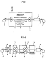
- the numeral 1 denotes a core wire; 2 denotes a supply mechanism; 3 denotes a preparatory processing mechanism; 4 denotes a continuous sputtering unit; 5 denotes a magnet; 6 denotes a target; and 7 denotes a winding mechanism.
- Said round wire was drawn again using a cold working die to change its diameter to 20 ⁇ m.
- the degree of cold working was 56 %.
- the wire drawing was smoothly effected with very few wire breaks.
- the weight per wire break was 5.3 times as much as when drawing a material obtained by a conventional method. Further, according to the method used in this example, the yield was high.
- the surface of the wire of 20 ⁇ m in diameter formed in the manner described above was coated with copper by sputtering to change its outer diameter to 30 ⁇ m, whereupon the wire was drawn to change its diameter 20 ⁇ m.
- the result was the same as described above.
- Enamel was applied by baking to the surface of the copper wire of 20 ⁇ m in diameter obtained in Example 1, whereby the wire was processed into a magnet wire.
- the magnet wire thus obtained had a good elongation property. That is, whereas the elongation of a magnet wire obtained by a conventional method was 16 %, the magnet wire obtained by the invention exhibited an elongation value of as high as 20 % while having substantially the same strength as said magnet wire obtained by a conventional method.
- a core wire denotes a core wire
- 12 denotes a supply mechanism
- 13 denotes a preparatory processing unit
- 14 denotes a die
- 16 denotes a driving mechanism
- 17 denotes a winding mechanism.
- the aluminum wire thus obtained was used as a bonding wire for wiring semiconductor elements; the bonding wire was found to exhibit a good corrosion resistance and bonding characteristic.
- a copper wire of 99.99 % purity was coated with copper of 99.999 % by vacuum vapor deposition.
- the conductor thus obtained was cold-worked using a die so that the percentage reduction in cross-sectional area was 70 %.
- Fig. 3 shows the cross section of the wire 101 thus obtained.
- the core 102 is copper of 99.99 %, while the surface area 103 is copper of 99.999 %.
- the outer diameter is 0.12 mm and the thickness of the coating of high purity copper is 0.01 mm.
- this conductor 101 for wiring a VTR, 7 such conductors were twisted together to form an electrical wire, as shown in Fig. 4.
- the sounds and images of the VTR were compared with those obtained by an electrical wire formed of conductors of the same diameter made of a soft material of conventional oxygen-free copper. It was found that when the conductor 101 which is an example of the invention obtained in the manner described above was used, the sounds were very rich and clear and the images were clear.
- the surface of a copper wire of 99.99 % was coated with copper of 99.999 % by plasma CVD method to provide a tape-like conductor 104 as shown in Fig. 5.
- the conductor was then punched and used as a lead for transistors in stereos. As compared with a lead of conventional oxygen-free copper, this lead provided clear sounds and sound effects of good quality.
- the surface of a copper wire of 90 ⁇ m in diameter having a purity of 99.99 % was coated with copper of 99.9998 % purity by sputtering until its diameter was 100 ⁇ m. It was then drawn until its diameter was 25 ⁇ m for use as a bonding wire.
- This bonding wire was bonded to an Al vapor deposition electrode by ball bonding method making a ball by arc discharge method in an Ar atmosphere. It was found that the wedge bonding area between the bonding wire and the ball bonding area and the wedge bonding area between the bonding wire and an Al-plated lead frame portion were both superior in bonding characteristic.
Landscapes
- Chemical & Material Sciences (AREA)
- Engineering & Computer Science (AREA)
- Chemical Kinetics & Catalysis (AREA)
- Materials Engineering (AREA)
- Mechanical Engineering (AREA)
- Metallurgy (AREA)
- Organic Chemistry (AREA)
- Manufacturing & Machinery (AREA)
- Wire Bonding (AREA)
- Physical Vapour Deposition (AREA)
- Metal Extraction Processes (AREA)
- Conductive Materials (AREA)
Claims (3)
- Einen dünnen Draht aufweisender elektrischer Leiter, der einen Metall-Kernleiter und eine leitende Metall-Beschichtung auf dem Metall-Kernleiter aufweist, wobei- der Metall-Kernleiter aus einem Metall hergestellt ist, das aus der Gruppe aus Kupper, Aluminium und Gold ausgewählt ist,- die leitende Metallbeschichtung aus dem gleichen Metall wie der Metall-Kernleiter hergestellt ist und eine höhergradige Reinheit wie der Meallkernleiter hat,- der Metall-Kernleiter eine Reinheit von wenigstens 99,99 % hat,- die leitende Metallbeschichtung eine Reinheit von wenigstens 99,999 % hat, und- der elektrische Leiter, der den Metall-Kernleiter und die leitende Metallbeschichtung umfaßt, einen Außendurchmesser im Bereich von etwa 20 µm bis etwa 127 µm hat.
- Verfahren zur Herstellung eines eines dünnen Draht aufweisenden elektrischen Leiters mit einem bestimmten Enddurchmesser, welches folgende Schritte umfaßt:a) Bilden eines Metall-Kernleiters aus reinem Metall aus der Gruppe von Kupfer, Aluminium und Gold, mit einer Reinheit von wenigstens 99,99 %, wobei der Metall-Kernleiter einen Ausgangsdurchmesser aufweist,b) Aufbringen einer leitenden Metallbeschichtung aus dem gleichen Metall wie das des Metall-Kernleiters, das eine höhere Reinheit als das Metall des Metall-Kernleiters hat, wobei die Reinheit wenigstens 99,999 % beträgt, auf den Metall-Kernleiter durch Ausscheiden aus der Dampfphase, um eine beschichteten Draht zu bilden, der einen zweiten Durchmesser hat, der größer als der Ausgangsdurchmesser des Metall-Kernleiters ist, undc) Kaltverformen des beschichteten Drahtes zur plastischen Verringerung des Durchmessers des beschichteten Drahtes, um so eine prozentuale Verringerung der Querschnittsfläche des beschichteten Drahtes im Bereich von 20-90 % zu erzielen, um einen fertigen Draht herzustellen, der einen Enddurchmesser hat, der im Bereich von etwa 20 µm bis etwa 127 um liegt.
- Verfahren nach Anspruch 2, wobei das Aufbringen der leitenden Metallbeschichtung und die Kaltverformungschritte im Wechsel mehrere Male durchgeführt werden.
Applications Claiming Priority (6)
| Application Number | Priority Date | Filing Date | Title |
|---|---|---|---|
| JP61061898A JPS62220237A (ja) | 1986-03-18 | 1986-03-18 | 金属細線の製造方法 |
| JP61898/86 | 1986-03-18 | ||
| JP131624/86 | 1986-06-05 | ||
| JP13162486A JPH0673250B2 (ja) | 1986-06-05 | 1986-06-05 | 音響・画像機器用導体およびその製造方法 |
| JP132434/86 | 1986-06-06 | ||
| JP61132434A JPH0795553B2 (ja) | 1986-06-06 | 1986-06-06 | 半導体素子の結線用ボンデイングワイヤおよびその製造方法 |
Publications (2)
| Publication Number | Publication Date |
|---|---|
| EP0241721A1 EP0241721A1 (de) | 1987-10-21 |
| EP0241721B1 true EP0241721B1 (de) | 1992-09-23 |
Family
ID=27297676
Family Applications (1)
| Application Number | Title | Priority Date | Filing Date |
|---|---|---|---|
| EP87103688A Expired - Lifetime EP0241721B1 (de) | 1986-03-18 | 1987-03-13 | Leiter und Verfahren zum Herstellen desselben |
Country Status (4)
| Country | Link |
|---|---|
| US (2) | US4815309A (de) |
| EP (1) | EP0241721B1 (de) |
| KR (1) | KR900007567B1 (de) |
| DE (1) | DE3781822T2 (de) |
Families Citing this family (11)
| Publication number | Priority date | Publication date | Assignee | Title |
|---|---|---|---|---|
| US5765418A (en) * | 1994-05-16 | 1998-06-16 | Medtronic, Inc. | Method for making an implantable medical device from a refractory metal |
| US6610930B1 (en) * | 1998-09-16 | 2003-08-26 | Kulicke & Soffa Investments, Inc. | Composite noble metal wire |
| US6696756B2 (en) * | 2001-07-16 | 2004-02-24 | Tao-Kuang Chang | Gold wire for use in semiconductor packaging and high-frequency signal transmission |
| WO2004113584A1 (en) * | 2002-12-23 | 2004-12-29 | Pirelli Pneumatici S.P.A. | Method dor producing coated metal wire |
| ES2294490T3 (es) * | 2004-03-31 | 2008-04-01 | Pirelli Tyre S.P.A. | Proceso de produccion de un hilo metalico revestido mediante una tecnica de deposicion por plasma. |
| BRPI0418686B1 (pt) | 2004-03-31 | 2013-07-23 | método e aparelho para produzir um fio de aço revestido | |
| EP1776488B1 (de) * | 2004-06-30 | 2016-04-13 | NV Bekaert SA | Verfahren zur herstellung eines mit einer messingschicht überzogenen metalldrahts |
| DE102006060899A1 (de) * | 2006-12-20 | 2008-07-10 | Micro-Systems-Engineering Gmbh & Co. Kg | Anschlussdraht, Verfahren zur Herstellung eines solchen und Baugruppe |
| RU2412792C1 (ru) * | 2009-09-08 | 2011-02-27 | Открытое Акционерное Общество Объединение "Мастер" | Биметаллическая электродная проволока, способ изготовления биметаллической электродной проволоки и устройство для изготовления биметаллической электродной проволоки |
| TW201545828A (zh) * | 2014-06-10 | 2015-12-16 | Ya-Yang Yan | 一種放電加工切割線及該放電加工切割線之製造方法 |
| US20240105668A1 (en) * | 2021-02-05 | 2024-03-28 | Nippon Micrometal Corporation | Ai wiring material |
Family Cites Families (19)
| Publication number | Priority date | Publication date | Assignee | Title |
|---|---|---|---|---|
| DE314791C (de) * | ||||
| US1810499A (en) * | 1928-12-04 | 1931-06-16 | Rca Corp | Transformer winding wire |
| GB343163A (en) * | 1929-11-15 | 1931-02-16 | Willoughby Statham Smith | Submarine cables |
| GB804900A (en) * | 1956-03-03 | 1958-11-26 | Ernst Weisse | Improvements in composite plated aluminium alloy material |
| US2984894A (en) * | 1956-11-30 | 1961-05-23 | Engelhard Ind Inc | Composite material |
| DE1172922B (de) * | 1962-03-24 | 1964-06-25 | Ver Leichtmetallwerke Gmbh | Dreischichtiger Verbundwerkstoff aus Aluminiumwerkstoffen |
| GB1007260A (en) * | 1963-02-27 | 1965-10-13 | Imp Smelting Corp Ivsc Ltd | Alloy-clad metal |
| US3926573A (en) * | 1970-09-18 | 1975-12-16 | Texas Instruments Inc | Composite wire and method of making |
| BE762681A (nl) * | 1971-02-09 | 1971-07-16 | Bekaert Sa Nv | Inrichting voor het opdampen van een metalen deklaag op een langwerpig substraat met behulp van tenminste een elektronenkanon. |
| GB1425754A (en) * | 1973-07-03 | 1976-02-18 | Electricity Council | Methods of and apparatus for coating wire rod or strip material by sputtering |
| GB1489510A (en) * | 1976-05-28 | 1977-10-19 | Delta Enfield Cables Ltd | Method of manufacturing cable conductors |
| JPS5497514A (en) * | 1978-01-19 | 1979-08-01 | Sumitomo Electric Ind Ltd | Aluminum alloy composite |
| FR2442494A1 (fr) * | 1978-11-24 | 1980-06-20 | Alsthom Atlantique | Piece conductrice electrique a isolation resistant a des temperatures elevees et procede de fabrication de celle-ci |
| US4234622A (en) * | 1979-04-11 | 1980-11-18 | The United States Of American As Represented By The Secretary Of The Army | Vacuum deposition method |
| DE2937783A1 (de) * | 1979-09-19 | 1981-03-26 | Otto Ing.(grad.) 8500 Nürnberg Breitenbach | Flexible elektrische flachbandleitung |
| JPS5835589B2 (ja) * | 1979-09-19 | 1983-08-03 | 住友軽金属工業株式会社 | 熱交換器用アルミニウム合金合わせ材 |
| JPS5976453A (ja) * | 1982-10-19 | 1984-05-01 | Mitsubishi Metal Corp | 半導体装置のリ−ド材用Cu合金クラツド材 |
| JPS604255B2 (ja) * | 1982-10-21 | 1985-02-02 | 日本国有鉄道 | トロリ−線 |
| JPS59143040A (ja) * | 1983-02-04 | 1984-08-16 | Kobe Steel Ltd | 溶接構造用Al合金 |
-
1987
- 1987-03-13 EP EP87103688A patent/EP0241721B1/de not_active Expired - Lifetime
- 1987-03-13 US US07/025,607 patent/US4815309A/en not_active Expired - Lifetime
- 1987-03-13 DE DE8787103688T patent/DE3781822T2/de not_active Expired - Fee Related
- 1987-03-16 KR KR1019870002335A patent/KR900007567B1/ko not_active Expired
-
1988
- 1988-05-10 US US07/192,397 patent/US4859811A/en not_active Expired - Lifetime
Also Published As
| Publication number | Publication date |
|---|---|
| KR900007567B1 (ko) | 1990-10-15 |
| EP0241721A1 (de) | 1987-10-21 |
| US4859811A (en) | 1989-08-22 |
| US4815309A (en) | 1989-03-28 |
| KR870009409A (ko) | 1987-10-26 |
| DE3781822T2 (de) | 1993-01-07 |
| DE3781822D1 (de) | 1992-10-29 |
Similar Documents
| Publication | Publication Date | Title |
|---|---|---|
| EP0241721B1 (de) | Leiter und Verfahren zum Herstellen desselben | |
| US4279967A (en) | Soft copper alloy conductors and their method of manufacture | |
| JP2002121629A (ja) | 超極細銅合金線、銅合金撚線導体、極細同軸ケーブル、および超極細銅合金線の製造方法 | |
| US4755235A (en) | Electrically conductive precipitation hardened copper alloy and a method for manufacturing the same | |
| EP0234071B1 (de) | Verfahren zum Herstellen eines supraleitenden elektrischen Leiters | |
| JPH0790430A (ja) | 極細線用銅線,及びその製造方法 | |
| JPH0435538B2 (de) | ||
| JPH0259109A (ja) | チタン極細線の製造方法 | |
| JP3405069B2 (ja) | 放電加工用電極線 | |
| JPS5910522B2 (ja) | 銅被覆アルミニウム線 | |
| JP2001181811A (ja) | クロム・ジルコニウム系銅合金線の製造方法 | |
| JP2996378B2 (ja) | 冷間圧延によって圧延される導電線用銅合金ロッドの製造法 | |
| JPH05311364A (ja) | 高強度高導電性銅合金の製造方法 | |
| JPH0917237A (ja) | 銅又は銅合金被覆アルミニウム合金線 | |
| RU2559803C2 (ru) | СПОСОБ ИЗГОТОВЛЕНИЯ КОМПОЗИЦИОННОГО СВЕРХПРОВОДЯЩЕГО ПРОВОДА НА ОСНОВЕ СОЕДИНЕНИЯ Nb3Sn И ТЕХНОЛОГИЧЕСКАЯ ЛИНИЯ ДЛЯ ИЗГОТОВЛЕНИЯ КОМПОЗИЦИОННОГО СВЕРХПРОВОДЯЩЕГО ПРОВОДА НА ОСНОВЕ СОЕДИНЕНИЯ Nb3Sn | |
| JPS62220237A (ja) | 金属細線の製造方法 | |
| JP2915596B2 (ja) | 極細線の製造方法 | |
| JP3858861B2 (ja) | 架空配電線用銅線及びその製造方法 | |
| JPH05267090A (ja) | 耐熱高導電性複合線状体 | |
| JPH0795553B2 (ja) | 半導体素子の結線用ボンデイングワイヤおよびその製造方法 | |
| JPS5931857A (ja) | ワイヤカツト放電加工用電極線の製造法 | |
| JP2996379B2 (ja) | 冷間圧延によって圧延される導電線用銅合金ロッドの製造方法 | |
| JPS60125359A (ja) | 画像表示機器、音響機器用導体の製造法 | |
| JP2991319B2 (ja) | 高強度・高導電性銅合金及び製造方法(2) | |
| JPH10140268A (ja) | 高強度及び高電導性の複合銅合金材料 |
Legal Events
| Date | Code | Title | Description |
|---|---|---|---|
| PUAI | Public reference made under article 153(3) epc to a published international application that has entered the european phase |
Free format text: ORIGINAL CODE: 0009012 |
|
| AK | Designated contracting states |
Kind code of ref document: A1 Designated state(s): DE FR GB |
|
| RIN1 | Information on inventor provided before grant (corrected) |
Inventor name: NAKAI, YOSHIHIRO OSAKA WORKS Inventor name: NISHIO, MASANOBU OSAKA WORKS Inventor name: SAWADA,KAZUO OSAKA WORKS |
|
| 17P | Request for examination filed |
Effective date: 19880414 |
|
| RAP1 | Party data changed (applicant data changed or rights of an application transferred) |
Owner name: SUMITOMO ELECTRIC INDUSTRIES, LTD. |
|
| 17Q | First examination report despatched |
Effective date: 19900607 |
|
| GRAA | (expected) grant |
Free format text: ORIGINAL CODE: 0009210 |
|
| AK | Designated contracting states |
Kind code of ref document: B1 Designated state(s): DE FR GB |
|
| REF | Corresponds to: |
Ref document number: 3781822 Country of ref document: DE Date of ref document: 19921029 |
|
| ET | Fr: translation filed | ||
| PLBE | No opposition filed within time limit |
Free format text: ORIGINAL CODE: 0009261 |
|
| STAA | Information on the status of an ep patent application or granted ep patent |
Free format text: STATUS: NO OPPOSITION FILED WITHIN TIME LIMIT |
|
| 26N | No opposition filed | ||
| PGFP | Annual fee paid to national office [announced via postgrant information from national office to epo] |
Ref country code: DE Payment date: 20010306 Year of fee payment: 15 |
|
| PGFP | Annual fee paid to national office [announced via postgrant information from national office to epo] |
Ref country code: GB Payment date: 20010307 Year of fee payment: 15 |
|
| PGFP | Annual fee paid to national office [announced via postgrant information from national office to epo] |
Ref country code: FR Payment date: 20010313 Year of fee payment: 15 |
|
| REG | Reference to a national code |
Ref country code: GB Ref legal event code: IF02 |
|
| PG25 | Lapsed in a contracting state [announced via postgrant information from national office to epo] |
Ref country code: GB Free format text: LAPSE BECAUSE OF NON-PAYMENT OF DUE FEES Effective date: 20020313 |
|
| PG25 | Lapsed in a contracting state [announced via postgrant information from national office to epo] |
Ref country code: DE Free format text: LAPSE BECAUSE OF NON-PAYMENT OF DUE FEES Effective date: 20021001 |
|
| GBPC | Gb: european patent ceased through non-payment of renewal fee |
Effective date: 20020313 |
|
| PG25 | Lapsed in a contracting state [announced via postgrant information from national office to epo] |
Ref country code: FR Free format text: LAPSE BECAUSE OF NON-PAYMENT OF DUE FEES Effective date: 20021129 |
|
| REG | Reference to a national code |
Ref country code: FR Ref legal event code: ST |