EP0239386A2 - Kraftmessdose und Temperaturkorrektur derselben - Google Patents
Kraftmessdose und Temperaturkorrektur derselben Download PDFInfo
- Publication number
- EP0239386A2 EP0239386A2 EP87302580A EP87302580A EP0239386A2 EP 0239386 A2 EP0239386 A2 EP 0239386A2 EP 87302580 A EP87302580 A EP 87302580A EP 87302580 A EP87302580 A EP 87302580A EP 0239386 A2 EP0239386 A2 EP 0239386A2
- Authority
- EP
- European Patent Office
- Prior art keywords
- thin film
- resistor
- zero point
- temperature
- load cell
- Prior art date
- Legal status (The legal status is an assumption and is not a legal conclusion. Google has not performed a legal analysis and makes no representation as to the accuracy of the status listed.)
- Withdrawn
Links
Images

Classifications
-
- G—PHYSICS
- G01—MEASURING; TESTING
- G01L—MEASURING FORCE, STRESS, TORQUE, WORK, MECHANICAL POWER, MECHANICAL EFFICIENCY, OR FLUID PRESSURE
- G01L1/00—Measuring force or stress, in general
- G01L1/20—Measuring force or stress, in general by measuring variations in ohmic resistance of solid materials or of electrically-conductive fluids; by making use of electrokinetic cells, i.e. liquid-containing cells wherein an electrical potential is produced or varied upon the application of stress
- G01L1/22—Measuring force or stress, in general by measuring variations in ohmic resistance of solid materials or of electrically-conductive fluids; by making use of electrokinetic cells, i.e. liquid-containing cells wherein an electrical potential is produced or varied upon the application of stress using resistance strain gauges
- G01L1/2206—Special supports with preselected places to mount the resistance strain gauges; Mounting of supports
- G01L1/2243—Special supports with preselected places to mount the resistance strain gauges; Mounting of supports the supports being parallelogram-shaped
-
- G—PHYSICS
- G01—MEASURING; TESTING
- G01L—MEASURING FORCE, STRESS, TORQUE, WORK, MECHANICAL POWER, MECHANICAL EFFICIENCY, OR FLUID PRESSURE
- G01L1/00—Measuring force or stress, in general
- G01L1/20—Measuring force or stress, in general by measuring variations in ohmic resistance of solid materials or of electrically-conductive fluids; by making use of electrokinetic cells, i.e. liquid-containing cells wherein an electrical potential is produced or varied upon the application of stress
- G01L1/22—Measuring force or stress, in general by measuring variations in ohmic resistance of solid materials or of electrically-conductive fluids; by making use of electrokinetic cells, i.e. liquid-containing cells wherein an electrical potential is produced or varied upon the application of stress using resistance strain gauges
- G01L1/2268—Arrangements for correcting or for compensating unwanted effects
- G01L1/2281—Arrangements for correcting or for compensating unwanted effects for temperature variations
Definitions
- This invention relates to a load cell for use with an electronic weighing instrument or the like, and more particularly to a load cell having a fixed characteristic which is not influenced by a temperature change and also to a method of correcting such a load cell for temperature.
- an insulator film is first formed on a surface of a beam member, and then a resistor film and a conductor film are formed in layers on the insulator film by evaporation, sputtering or a like process and are then selectively etched to form strain gauges at locations of the insulator film adjacent thin film deformable portions of the beam member whereafter leads for electric connection are formed on the insulator film to complete a bridge circuit of the thin film strain gauges.
- Some of such conventional load cells include a zero point balance correcting resistor connected to such a bridge circuit of strain gauges.
- load cells require correction for temperature with respect to a zero point balance and a span thereof. This is because resistances of such strain gauges vary as the temperature changes.
- temperature correction for the zero point balance is attained by adjusting a length of a thin copper wire while temperature correction for the span is attained by trimming, using a cutter or the like, a Ni film resistor which is formed by rolling a Ni wire or Ni and applying the rolled Ni wire or Ni to an insulator film on a beam member.
- a load cell comprises a span resistor member and a zero point resistor member both formed separately of the beam member and including a span temperature correcting thin film resistor and a zero point balance temperature correcting thin film resistor, respectively, each of which has a temperature coefficient and is formed on a substrate.
- the resistor members are applied to the insulator film on the beam member and the film resistors are connected to a bridge circuit.
- the thin film resistors are trimmed with a laser beam to correct the span temperature correcting thin film resistor and the zero point balance temperature correcting thin film resistor for temperature.
- the beam member under the insulator film will not be trimmed due to the presence of the substrates of the resistor members on the insulator film. Accordingly, trimming can be achieved readily without damaging the insulation of the load cell.
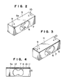
- a load cell according to the invention includes a beam member 5 as generally shown in Fig. 2.
- the beam member 5 is in the form of an elastic rectangular parallelepiped made of a metal material such as duralumin and having a substantially 8-shaped transverse hole 6 formed in a vertical wall thereof by machining thereby to define four upper and lower thin material deformable portions 7.
- An upper face of the beam member 5 is constituted as a bridge circuit forming face 5a which will be hereinafter described and is hence polished into a flat face.
- the beam member 5 has a pair of mounting holes 9 formed at an end portion thereof for mounting the entire load cell to a support while another pair of mounting holes 10 are formed at the other end portion of the beam member 5 for mounting a load receiving plate.
- An insulator film 11 is formed directly on the circuit forming face 5a of the beam member 5 as shown in Fig. 3.
- the insulator film 11 may be formed from an inorganic insulating material such as, for example, SiO2 or else from an organic insulating material such as, for example, a polyimide resin.
- the insulator film 11 has a sufficiently small thickness of, for example, several to several tens microns so that it may not have an influence on the sensitivity of the thin material deformable portions 7 of the beam member 5.
- the first layer 12 may be formed from a thin resistor film of NiCr or the like to be used for a strain gauge resistor thin film and also for a zero point balance correcting resistor thin film and may be produced by a thin film forming technique such as evaporation, sputtering or plating.
- the second layer 13 may be formed from a thin conductor film of Cu or the like to be used for leads for electric connection and may similarly be produced by a thin film forming technique such as evaporation or the like.
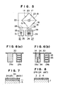
- the first and second layers 12, 13 are selectively etched into predetermined patterns by photoetching or the like. Consequently, as illustratively shown in Fig. 1, four thin material strain gauges 14 to 17 and a zero point balance correcting resistor 18 are formed from the first layer 12 such that the four thin material strain gauges 14 to 17 are located on upper ones of the four thin material deformable portions 7 of the beam member 5 and the zero point balance correcting resistor 18 is located near the thin film strain gauge 14 while leads 19 for electrically connecting the thin material strain gauges 14 to 17 and the zero balance correcting resistor 18 into a bridge are formed from the second layer.
- a bridge circuit 20 (refer to Fig. 5) is formed in this manner. Leads 19 are also formed for input/output terminals 21.
- the input/output terminals 21 are connected to an input power source 22 and an output device 23 such as an amplifier of the circuit shown in Fig. 5.
- the two adjacent thin material strain gauges 15, 16 in the bridge circuit 20 are not directly connected to each other but a zero point balance temperature correcting thin film resistor 24 is interposed therebetween.
- a span temperature correcting thin film resistor 25 is also interposed between the zero point balance temperature correcting thin film resistor 24 and the input power source 22.
- the zero point balance temperature correcting thin film resistor 24 is formed on a substrate 26 as a zero point balance resistor member 27.
- the substrate 26 of the zero point balance resistor member 27 is applied to the insulator film 11 on the beam member 5, and the zero point balance temperature correcting thin film resistor 24 is connected to the thin material strain gauges 15, 16 by connecting terminals 28 formed on the leads 19 from the thin material strain gauges 15, 16 to terminals 29 formed on the zero point balance temperature correcting thin film resistor 24 side.
- the zero point balance temperature correcting thin film resistor 24 is formed by forming a resistor thin film of a metal having a temperature coefficient such as Ni or Ti on the substrate 26 formed from a thin film substrate of a ceramics material or the like by evaporation, sputtering or the like and by etching the metal resistor thin film into a predetermined pattern.
- the zero point balance temperature correcting thin film resistor 24 in the present embodiment, it is divided into two thin film resistors including a thin film resistor 24a of a filled up rectangular pattern and the other thin film resistor 24b of a ladder-shaped pattern as shown in Figs. 1 and 6(a).
- the thin film resistors 24a, 24b are connected in series by a lead 30, and three terminals 29 extend from an intermediate point and opposite ends of the lead 30.
- the span temperature correcting thin film resistor 25 is similar to the zero point balance temperature correcting thin film resistor 24 and is formed on a substrate 31 and thus formed as a span resistor member 32 as particularly shown in a partially enlarged view in Fig. 1.
- the substrate 31 is applied to the insulator film 1, and the span temperature correcting thin film resistor 25 is connected to the bridge circuit by connecting terminals 33 formed on the span temperature correcting thin film resistor 25 side to the central one of the terminals 29 of the zero point balance temperature correcting thin film resistor 24 and to that one of the terminals 28 which extends from the input power source 22.
- the span temperature correcting thin film resistor 25 is also produced by forming a resistor thin film of a metal having a temperature coefficient such as Ni or Ti on the substrate 31 formed from a thin film substrate such as a ceramics material or the like by evaporation, sputtering or the like and by etching the metal resistor thin film into a predetermined pattern such as, for example, a filled up rectangular pattern.
- a resistor thin film of a metal having a temperature coefficient such as Ni or Ti on the substrate 31 formed from a thin film substrate such as a ceramics material or the like by evaporation, sputtering or the like and by etching the metal resistor thin film into a predetermined pattern such as, for example, a filled up rectangular pattern.
- the substrates 26, 31 may be applied to the insulator film 11 using a bonding agent or the like and are located at such positions at which they may not have a bad influence on deformation of the beam member 5 and particularly at positions other than the thin material deformable portions 7 of the beam member 5.
- the span resistor member 32 and the zero point balance resistor member 27 are applied to the insulator film 11 and connected to the bridge circuit 20 in this manner, temperature correction of the load cell is achieved.
- a temperature of the beam member 5 is detected to measure a temperature characteristic of the zero point balance and a temperature characteristic of the span, and then correction values are calculated from results of such measurements whereafter the zero point balance temperature correcting thin film resistor 24 and the span temperature correcting thin film resistor 25 are trimmed by a laser beam so that they may have individual predetermined resistances.
- the zero point balance temperature correcting thin film resistor 24 and the span temperature correcting thin film resistor 25 are trimmed by a laser beam so that they may have individual predetermined resistances.
- the zero point balance temperature correcting thin film resistor 24 it is trimmed to change the initial pattern thereof as shown in Fig. 6(a) to another pattern as shown in Fig.
- a serial resistance can be changed by changing trimmed portions 34 at the thin film resistor 24a while a parallel resistance can be changed by changing trimmed portions 35 at the thin film resistor 24b. Accordingly, fine correction in resistance can be attained for the entire zero point balance temperature correcting thin film resistance 24. Particularly by correction of the serial resistance by the trimmed portions 34 at the thin film resistors 24a, an adjustment in resistance in an analog manner can be attained. Accordingly, the correction can be achieved with high accuracy. It is to be noted that laser trimming may be achieved for the span temperature correcting thin film resistor 25 in a similar procedure to that for the thin film resistor 24a.
- the zero point balance temperature correcting thin film resistor 24 (or span temperature correcting thin film resistor 25) can be trimmed with accuracy while the insulator film 11 as well as the beam member 5 can be prevented readily from being trimmed, and accordingly the insulation of the load cell will not be damaged.
- a coating or the like for prevention of humidity is formed over an upper face of the load cell.
- temperature correction of the load cell can be achieved with high operability by applying and connecting to the insulator film 11 of the beam member 5 the span resistor member 32 and the zero point balance resistor member 27 which are both prepared as separate pieces from the beam member 5 and by laser trimming the span resistor member 32 and the zero point balancing resistor member 27. Further, since the substrates 26, 31 of the zero point balance resistor member 27 and the span resistor member 32, respectively, are present on the insulator film 11 when trimming is achieved, accurate trimming can be achieved without a fear of damaging the insulation of the load cell.
- the resistor members 27, 32 which are formed as separate pieces from the beam member 5
- the number of operations for sputtering when the thin material strain gauges 14 to 17 and so on are produced from a thin film can be reduced.
- the substrates 26, 31 are formed from a ceramics material, even if they have a reduced thickness, they will not be deformed readily and will have a high insulation.
- the two substrates 26, 31 may be formed into a single substrate on which both of the zero point balance temperature correcting thin film resistor 24 and the span temperature correcting thin film resistor 25 are formed.
Landscapes
- Physics & Mathematics (AREA)
- General Physics & Mathematics (AREA)
- Measurement Of Force In General (AREA)
Applications Claiming Priority (2)
| Application Number | Priority Date | Filing Date | Title |
|---|---|---|---|
| JP61070196A JPS62226029A (ja) | 1986-03-28 | 1986-03-28 | ロ−ドセルの温度補正方法 |
| JP70196/86 | 1986-03-28 |
Publications (2)
| Publication Number | Publication Date |
|---|---|
| EP0239386A2 true EP0239386A2 (de) | 1987-09-30 |
| EP0239386A3 EP0239386A3 (de) | 1989-07-26 |
Family
ID=13424521
Family Applications (1)
| Application Number | Title | Priority Date | Filing Date |
|---|---|---|---|
| EP87302580A Withdrawn EP0239386A3 (de) | 1986-03-28 | 1987-03-25 | Kraftmessdose und Temperaturkorrektur derselben |
Country Status (4)
| Country | Link |
|---|---|
| US (1) | US4747456A (de) |
| EP (1) | EP0239386A3 (de) |
| JP (1) | JPS62226029A (de) |
| CA (1) | CA1275661C (de) |
Cited By (5)
| Publication number | Priority date | Publication date | Assignee | Title |
|---|---|---|---|---|
| WO1992008115A1 (en) * | 1990-11-01 | 1992-05-14 | Eastman Kodak Company | Thin film precision load cell |
| EP0534226A1 (de) * | 1991-09-24 | 1993-03-31 | Kabushiki Kaisha TEC | Dehnungssensor mit einer Dehnungsmessstreifenschaltung und Kraftmesszellenwaage mit diesem Dehnungssensor |
| DE19747001A1 (de) * | 1997-10-24 | 1999-05-12 | Mannesmann Vdo Ag | Elektrischer Widerstand sowie ein mit diesem elektrischen Widerstand hergestellter mechanisch elektrischer Wandler |
| CN104931118A (zh) * | 2014-03-21 | 2015-09-23 | 梅特勒-托利多(常州)精密仪器有限公司 | 应变式称重传感器及其滞后补偿方法 |
| CN114777970A (zh) * | 2022-05-23 | 2022-07-22 | 电子科技大学 | 高刚度测力刀柄上基于柔性电路板的薄膜应变计电桥电路 |
Families Citing this family (32)
| Publication number | Priority date | Publication date | Assignee | Title |
|---|---|---|---|---|
| JPH0171633U (de) * | 1987-10-31 | 1989-05-12 | ||
| JPH0375535A (ja) * | 1989-08-18 | 1991-03-29 | Kubota Corp | トルクセンサ |
| JPH03233334A (ja) * | 1990-02-08 | 1991-10-17 | Nec Corp | 半導体圧力センサ |
| JPH0461009U (de) * | 1990-09-29 | 1992-05-26 | ||
| DE4128557A1 (de) * | 1991-08-28 | 1993-03-04 | Soehnle Waagen Gmbh & Co | Waegezelle fuer eine elektronische waage |
| US5623128A (en) * | 1994-03-01 | 1997-04-22 | Mettler-Toledo, Inc. | Load cell with modular calibration components |
| US5929390A (en) * | 1994-09-14 | 1999-07-27 | Ishida Co., Ltd. | Load cell weighing apparatus using the same |
| US5608173A (en) * | 1995-06-07 | 1997-03-04 | Sensor Developments, Inc. | Force measuring apparatus having electrically-insulated load bearing surfaces |
| DE19615499A1 (de) * | 1996-04-19 | 1997-10-23 | Vdo Schindling | Zeigerinstrument |
| JP3433439B2 (ja) * | 1996-06-26 | 2003-08-04 | 長野計器株式会社 | センシング素子 |
| US5734110A (en) * | 1996-10-11 | 1998-03-31 | Kistler-Morse Corporation | Temperature compensated, easily installed bolt-on strain sensor |
| US6134971A (en) * | 1998-08-27 | 2000-10-24 | University Of Hawaii | Stress induced voltage fluctuation for measuring stress and strain in materials |
| US6225576B1 (en) * | 1999-04-20 | 2001-05-01 | Cts Corporation | Shear beam load cell |
| US6677538B2 (en) * | 2000-02-25 | 2004-01-13 | Siemens Vdo Automotive Corporation | Signal processing in a vehicle weight classification system |
| GB2370122B (en) * | 2000-12-16 | 2005-04-27 | Senstronics Ltd | Temperature compensated strain gauge |
| JP3913526B2 (ja) * | 2001-10-30 | 2007-05-09 | 独立行政法人科学技術振興機構 | 変位センサとその製造方法および位置決めステージ |
| DE10355817A1 (de) * | 2003-11-28 | 2005-07-21 | Fag Kugelfischer Ag | Wälzlager mit einem System zur Datenerfassung und zur Datenverarbeitung |
| US9360383B2 (en) | 2013-04-04 | 2016-06-07 | Nate J. Coleman and Aexius, LLC | System and method to measure force or location on an L-beam |
| US8436261B2 (en) * | 2004-12-13 | 2013-05-07 | Nate John Coleman | Cantilever beam scale |
| DE102005060106B4 (de) * | 2005-12-16 | 2016-03-03 | Sartorius Lab Instruments Gmbh & Co. Kg | Präzisionskraftaufnehmer mit Dehnungsmesselementen |
| WO2008029648A1 (fr) * | 2006-09-05 | 2008-03-13 | Ishida Co., Ltd. | Module de cellules de charge, contrôleur de poids, et instrument de pesée électronique |
| KR101014537B1 (ko) * | 2008-07-04 | 2011-02-14 | 현대모비스 주식회사 | 자동차의 승객감지장치 |
| US9121258B2 (en) | 2010-11-08 | 2015-09-01 | Baker Hughes Incorporated | Sensor on a drilling apparatus |
| US9057247B2 (en) * | 2012-02-21 | 2015-06-16 | Baker Hughes Incorporated | Measurement of downhole component stress and surface conditions |
| JP6224065B2 (ja) * | 2012-03-29 | 2017-11-01 | レッド・ブル・ゲゼルシャフト・ミット・ベシュレンクテル・ハフツングRed Bull Gmbh | 貯蔵装置の取出し、充填、および/または充填状態を検出するための充填状態検出装置を有する品物用貯蔵装置 |
| ITTO20120293A1 (it) | 2012-04-03 | 2013-10-04 | Metallux Sa | Procedimento per tarare un elemento di calibrazione, e relativo dispositivo |
| WO2014165173A1 (en) * | 2013-03-12 | 2014-10-09 | Subsidence, Inc. | Mechanical strain-based weather sensor |
| CN105928644B (zh) * | 2016-06-29 | 2018-07-31 | 中交第二公路勘察设计研究院有限公司 | 一种用于路面结构监测的应变计 |
| CN106768215A (zh) * | 2017-03-24 | 2017-05-31 | 上海大和衡器有限公司 | 变形测定装置 |
| JP2019078726A (ja) * | 2017-10-27 | 2019-05-23 | ミネベアミツミ株式会社 | ひずみゲージ、センサモジュール |
| JP2019174387A (ja) | 2018-03-29 | 2019-10-10 | ミネベアミツミ株式会社 | ひずみゲージ |
| US12553782B2 (en) * | 2022-06-29 | 2026-02-17 | Subaru Corporation | Load cell and output adjustment method of load cell |
Family Cites Families (12)
| Publication number | Priority date | Publication date | Assignee | Title |
|---|---|---|---|---|
| US4158396A (en) * | 1977-04-22 | 1979-06-19 | Tokyo Electric Co., Ltd. | Electronic weight measuring device |
| JPS55140112A (en) * | 1979-04-19 | 1980-11-01 | Tokyo Electric Co Ltd | Weighing device employing load cell |
| AU534244B2 (en) * | 1979-04-19 | 1984-01-12 | Tokyo Electric Co. Ltd. | Load cell |
| US4299130A (en) * | 1979-10-22 | 1981-11-10 | Gould Inc. | Thin film strain gage apparatus with unstrained temperature compensation resistances |
| US4331035A (en) * | 1979-11-13 | 1982-05-25 | Gould Inc. | Geometric balance adjustment of thin film strain gage sensors |
| US4325048A (en) * | 1980-02-29 | 1982-04-13 | Gould Inc. | Deformable flexure element for strain gage transducer and method of manufacture |
| EP0053337B1 (de) * | 1980-11-29 | 1987-05-20 | Tokyo Electric Co., Ltd. | Lastmessvorrichtung und ihr Herstellungsverfahren |
| IT1137246B (it) * | 1981-06-10 | 1986-09-03 | Harris Pharma Ltd | Procedimento per la preparazione di un derivato del 2,4-diossacicloesanone |
| JPS5896202U (ja) * | 1981-12-23 | 1983-06-30 | 株式会社石田衡器製作所 | 歪みゲ−ジの温度補償回路 |
| JPS58208633A (ja) * | 1982-05-31 | 1983-12-05 | Tokyo Electric Co Ltd | 歪センサ |
| FR2542447B1 (fr) * | 1983-03-11 | 1985-10-18 | Electro Resistance | Capteur de force comprenant un support deformable et des jauges de contrainte |
| JPS60213837A (ja) * | 1984-04-09 | 1985-10-26 | Tokyo Electric Co Ltd | ロ−ドセル |
-
1986
- 1986-03-28 JP JP61070196A patent/JPS62226029A/ja active Pending
-
1987
- 1987-03-25 EP EP87302580A patent/EP0239386A3/de not_active Withdrawn
- 1987-03-26 CA CA000533022A patent/CA1275661C/en not_active Expired - Lifetime
- 1987-03-30 US US07/031,670 patent/US4747456A/en not_active Expired - Fee Related
Cited By (8)
| Publication number | Priority date | Publication date | Assignee | Title |
|---|---|---|---|---|
| WO1992008115A1 (en) * | 1990-11-01 | 1992-05-14 | Eastman Kodak Company | Thin film precision load cell |
| EP0534226A1 (de) * | 1991-09-24 | 1993-03-31 | Kabushiki Kaisha TEC | Dehnungssensor mit einer Dehnungsmessstreifenschaltung und Kraftmesszellenwaage mit diesem Dehnungssensor |
| DE19747001A1 (de) * | 1997-10-24 | 1999-05-12 | Mannesmann Vdo Ag | Elektrischer Widerstand sowie ein mit diesem elektrischen Widerstand hergestellter mechanisch elektrischer Wandler |
| DE19747001C2 (de) * | 1997-10-24 | 2000-02-24 | Mannesmann Vdo Ag | Dehnungsmeßstreifen sowie ein mit diesen Dehnungsmeßstreifen hergestellter mechanisch-elektrischer Wandler |
| CN104931118A (zh) * | 2014-03-21 | 2015-09-23 | 梅特勒-托利多(常州)精密仪器有限公司 | 应变式称重传感器及其滞后补偿方法 |
| CN104931118B (zh) * | 2014-03-21 | 2017-07-28 | 梅特勒-托利多(常州)精密仪器有限公司 | 应变式称重传感器及其滞后补偿方法 |
| CN114777970A (zh) * | 2022-05-23 | 2022-07-22 | 电子科技大学 | 高刚度测力刀柄上基于柔性电路板的薄膜应变计电桥电路 |
| CN114777970B (zh) * | 2022-05-23 | 2023-04-11 | 电子科技大学 | 高刚度测力刀柄上基于柔性电路板的薄膜应变计电桥电路 |
Also Published As
| Publication number | Publication date |
|---|---|
| JPS62226029A (ja) | 1987-10-05 |
| CA1275661C (en) | 1990-10-30 |
| US4747456A (en) | 1988-05-31 |
| EP0239386A3 (de) | 1989-07-26 |
Similar Documents
| Publication | Publication Date | Title |
|---|---|---|
| US4747456A (en) | Load cell and temperature correction of the same | |
| US4329878A (en) | Bridge circuit formed of two or more resistance strain gauges | |
| EP0053337B1 (de) | Lastmessvorrichtung und ihr Herstellungsverfahren | |
| US6097276A (en) | Electric resistor having positive and negative TCR portions | |
| US4628296A (en) | Load cell | |
| US8581687B2 (en) | Four-terminal resistor with four resistors and adjustable temperature coefficient of resistance | |
| US6188307B1 (en) | Thermistor apparatus and manufacturing method thereof | |
| US5548269A (en) | Chip resistor and method of adjusting resistance of the same | |
| JP3284375B2 (ja) | 電流検出用抵抗器及びその製造方法 | |
| US4748858A (en) | Strain gage transducer | |
| JPS592332B2 (ja) | ロ−ドセル秤 | |
| US3134953A (en) | Electric resistance devices | |
| US20010004848A1 (en) | Strain detector | |
| JP7783770B2 (ja) | 電流検出装置 | |
| JP2764517B2 (ja) | チップ抵抗器、ならびに、これを用いる電流検出回路および電流検出方法 | |
| JP3190120B2 (ja) | 計測用抵抗器およびその製造方法 | |
| US5039976A (en) | High-precision, high-stability resistor elements | |
| JPS5942402A (ja) | 歪センサの製造方法 | |
| GB2142776A (en) | Strain sensor | |
| JPS5942401A (ja) | 歪センサ | |
| GB2174241A (en) | Transducer devices | |
| JP2554881B2 (ja) | ロ−ドセル | |
| KR900004739B1 (ko) | 로우드 셀 | |
| JPH11160170A (ja) | 応力センサの製造方法 | |
| JPH05347202A (ja) | 電子部品及び電子部品の抵抗値調整方法 |
Legal Events
| Date | Code | Title | Description |
|---|---|---|---|
| PUAI | Public reference made under article 153(3) epc to a published international application that has entered the european phase |
Free format text: ORIGINAL CODE: 0009012 |
|
| AK | Designated contracting states |
Kind code of ref document: A2 Designated state(s): BE DE GB NL |
|
| PUAL | Search report despatched |
Free format text: ORIGINAL CODE: 0009013 |
|
| AK | Designated contracting states |
Kind code of ref document: A3 Designated state(s): BE DE GB NL |
|
| 17P | Request for examination filed |
Effective date: 19900105 |
|
| 17Q | First examination report despatched |
Effective date: 19910322 |
|
| STAA | Information on the status of an ep patent application or granted ep patent |
Free format text: STATUS: THE APPLICATION HAS BEEN WITHDRAWN |
|
| 18W | Application withdrawn |
Withdrawal date: 19921107 |
|
| RIN1 | Information on inventor provided before grant (corrected) |
Inventor name: KITAGAWA, TOHRU Inventor name: YAMASHITA, TAKAHARU |