EP0230730A2 - Machines pour calculer les CRC - Google Patents
Machines pour calculer les CRC Download PDFInfo
- Publication number
- EP0230730A2 EP0230730A2 EP86309177A EP86309177A EP0230730A2 EP 0230730 A2 EP0230730 A2 EP 0230730A2 EP 86309177 A EP86309177 A EP 86309177A EP 86309177 A EP86309177 A EP 86309177A EP 0230730 A2 EP0230730 A2 EP 0230730A2
- Authority
- EP
- European Patent Office
- Prior art keywords
- data
- input
- crc
- bits
- coupled
- Prior art date
- Legal status (The legal status is an assumption and is not a legal conclusion. Google has not performed a legal analysis and makes no representation as to the accuracy of the status listed.)
- Granted
Links
Images


Classifications
-
- H—ELECTRICITY
- H03—ELECTRONIC CIRCUITRY
- H03M—CODING; DECODING; CODE CONVERSION IN GENERAL
- H03M13/00—Coding, decoding or code conversion, for error detection or error correction; Coding theory basic assumptions; Coding bounds; Error probability evaluation methods; Channel models; Simulation or testing of codes
- H03M13/03—Error detection or forward error correction by redundancy in data representation, i.e. code words containing more digits than the source words
- H03M13/05—Error detection or forward error correction by redundancy in data representation, i.e. code words containing more digits than the source words using block codes, i.e. a predetermined number of check bits joined to a predetermined number of information bits
- H03M13/09—Error detection only, e.g. using cyclic redundancy check [CRC] codes or single parity bit
- H03M13/091—Parallel or block-wise CRC computation
Definitions
- the invention pertains to the field of cyclical redundancy codes calculation circuits for detecting errors in transmission of serial data over communication links. More particularly, the invention pertains to certain improvements in CRC calculation apparatus in integrated circuit form to conserve chip area.
- Error detection and correction using codes and check bits has long been used to improve the reliability of data transfers between units on a network or units in a computer system such as disk or main memory and the central processing unit.
- the most common scheme is parity checking.
- parity check bits are added to the information bits to make the total number of bits which are logic 1's in a byte equal to a known number.
- this scheme has the well known drawback that when the number of information bits becomes high, the level of redundancy in terms of check bits required becomes excessively high.
- Another checking scheme exists called polynomial or cyclic coding. This scheme can be designed to perform with higher efficiencies, i.e., less redundancy, than the parity checking schemes. The high efficiency of these schemes is inducing designers to use them more and more frequently.
- CRC bits cyclic code check bits
- another polynomial P(x) called a generating polynomial is chosen.
- the degree of this polynomial i.e., its highest exponent value, is greater than zero but less than the degree of M(x).
- the generator polynomial has a non-zero coefficient in x0 term. For a message of a given length, more than one generating polynomial can be specified.
- Cyclic check or CRC bit computation involves dividing the message polynomial by the generator polynomial to generate a quotient polynomial and a remainder polynomial. The quotient polynomial is discarded and the remainder polynomial coefficients are appended to the message polynomial as CRC check bits.
- the combined message and check bits are then transmitted over the communication link and arrive at the receiver either modified or unmodified depending upon whether errors occurred during the transmission.
- the receiving apparatus divides the complete received message, including check bits, by the same generator polynomial which was used to generate the check bits at the transmitter end of the link. The result of this division is a zero remainder polynomial if no error occurred during the transmission. A non-zero remainder indicates the presence of an error.
- Figure 1 is a block diagram of a CRC checkbit calculation machine.
- the CRC checksum register 30 is comprised of a plurality of memory cells that store the CRC check bits. The outputs of these memory cells are coupled to the inputs of an array 32 of shifting links some of which are exclusive-OR gates as best seen in Figure 2.
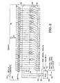
- Figure 2 is a detailed circuit diagram of the block diagram of Figure 1.
- the most significant output bit from the checksum register 30 is exclusive-ORed by an input gate 34 with the incoming serial data stream of the message polynomial, and the output of the exclusive-OR gate 34 which performs this function is coupled to an input of all the other exclusive-OR gates in the array.
- the array shifting links which are not exclusive-OR gates are simple conductors which merely shift the incoming data one bit position left or toward the most significant bit position.
- the outputs of the shifting links of the array are coupled back to the data inputs of the checksum register 30 by a bus 36.
- the exclusive-OR gates in the array 32 as well as the straight through conductors have their outputs coupled to the input of the checksum register of the next most significant bit position relative to the bit position of the input bits positions for each shifting link from the checksum register.
- a bit clock signal on the line 38 clocks the raw serial format input data of the message polynomial into the input gate 34 and causes the checksum register to load the data from the bus 36 into its memory cells. After all the raw input data bits in the message have been clocked in, the checksum register 30 contents are the CRC check bits for the message bits so processed.
- Figure 3 illustrates the format of the composite data packet that is transmitted after calculation of the checkbits.
- the segment 40 is the message polynomial upon which the CRC bits were calculated. These message polynomial bits are transmitted simultaneously with the calculation of the CRC bits in that each time a bit is input to the gate 34, it is simultaneously transmitted.
- the segment 42 is the complement of the CRC bits stored in the checksum register 30 after all the bits in the segment 40 have been processed.
- the segment 42 is comprised of complement CRC bits so that when CRC bits are calculated on the receiving end on the combined segments 40 and 42, the remainder will come out zero.
- the checksum register is preset to all logic 1's before the CRC calculation starts.
- the CRC checkbits in the segment 42 are sent following the segment 40 by switching a multiplexer 44 with a select signal on the line 47 to deselect the serial data input line 46 and select the output line 48 of an inverter 50.
- the input of the inverter 50 is coupled to the output of the most significant bit position memory cell in the checksum register.
- the inverter 50 inverts the check bits as they are clocked out in serial fashion by the bit clock signal on the line 38.
- the composite packet comprised of segment 40 followed by the CRC checkbits 42 appears on the serial output line 52.
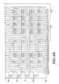
- the array of shifting links is comprised of a plurality of rows of shifting link with each row assigned to process one of the bits of the raw input data byte.
- the raw input data byte is shown as the bits D7 through D0 coupled to the input gates on the left.
- Each of these input data bits is coupled to an input of one of the input exclusive-OR gates 66, 68, 70, 72, 74, 76, 78 and 80.
- Each of these input gates has its output coupled to an input of each exclusive-OR gate in its row and to the input of the least significant bit position shifting link in the next row.
- each row in the array 56 acts like the shifting links row 32 in Figure 1 except that its outputs are connected to the inputs of the next row.
- the first row has its inputs coupled to the outputs of the checksum register 30 and the last row has its outputs coupled to the inputs of the checksum register.
- Each row has one input of its input gate coupled to the output of one of the bits in the highest order byte in the checksum register, the first row being connected to the highest order bit and the second row being connected to the second most signficant bit and so on for all the rows.
- Each shifting link in each row shifts its input bit one bit position toward the most significant bit position of the checksum register.
- the architecture of Figure 4 therefore calculates CRC bits by processing 8 bits of raw input data at a time.
- the first way is to calculate a header CRC on the header bits, and then to calculate a data CRC on the data message.
- the second way is to calculate a header CRC on the header bits, and then to calculate a data CRC on the whole packet including the header bits, the header CRC check bits and the data message. It would be useful to provide a CRC calculation machine which could calculate CRC checkbits using either of these two methods.
- a CRC calculation machine which can calculate CRC checkbits on both the header packet and the data packet separately where the CRC checkbits for the data packet are calculated either on the data packet alone or on the data packet plus the header packet plus the CRC bits for the header packet.
- the machine is comprised of a checksum register and an array of shifting links.
- the array of shifting links is a plurality of rows, one row for each bit of each input byte.
- the clock inputs of the checksum register memory cells are coupled to a byte clock signal which causes loading of data at the inputs of the checksum register periodically.
- the inputs of the checksum register are coupled to the outputs of the last row of the array of shifting links through an input multiplexer.
- the outputs of the checksum register are coupled to the data inputs of the first row of shifting links.
- Each row has one column or shifting link position for each bit in the checksum register.
- Some of the shifting links are exclusive-OR gates which have one input coupled to the output of an input gate.
- the other input of each exclusive-OR gate shifting link is coupled to an output bit of the checksum register for the column of that particular gate.
- the input gate for each row has one input coupled to one bit of the raw input data and one input coupled to one output of the checksum register in the most significant byte.
- the input gate for the first row in the array has one input coupled to the raw input data bit which would arrive first if the data were input in serial format.
- Another input of the input gate of the first row is coupled to the output of the most significant bit position memory cell in the checksum register.
- the second row input gate has one input coupled to the raw input data bit which would arrive second if the data were input in serial format.
- Another input of the input gate of the second row is coupled to the output of the second most significant bit position memory cell in the checksum register. This pattern is repeated for each row in the array.
- Each input gate performs an exclusive-OR function between one bit of the raw input data byte and one bit of the most significant byte of data stored in the checksum register.
- each exclusive-OR gate shifting link is coupled to the input of the shifting link in the next row in the next most significant bit position.
- the shifting links which are not exclusive-OR gates are conductors which conduct the bit at their inputs to the input of the shifting link in the next row in the next most significant bit position, i.e., they perform a simple one bit shift function and nothing more.
- the preferred embodiment uses an input multiplexer having its output coupled to the data inputs of the checksum register and having three inputs. One input is coupled to the outputs of the shifting links in the last row of the array. Another input is coupled to the data outputs of the checksum register. A third input is coupled to a predetermined bit pattern. This bit pattern represents the CRC checkbit pattern which results when a CRC calculation is performed on any data packet plus the CRC checkbits previously calculated on that data packet starting from a checksum register which has been preset to all logic ones.
- the input multiplexer has control inputs for receiving signals which control which of the inputs is selected at any particular time for coupling to the output of the multiplexer.
- the machine may be caused to calculate CRC bits on the header and data packets standing alone or may be forced to calculate the CRC bits on the data packet plus the header and the header CRC bits.
- the input of the input multiplexer connected to the remainder bit pattern is selected at a time after the CRC bits on the header have been calculated and these CRC bits have been shifted out and just before the first clock cycle of the interval where the data packet is input to the array.
- a snapshot register is coupled between the outputs of the last row of the array and the data input of the multiplexer normally coupled to the data outputs of the last row of the array.
- the snapshot register is clocked to make a copy of the CRC bits calculated on the header after they have been calculated.
- the CRC bits for the header are then either output or multiplexed back into the data inputs of the array through a multiplexer which channels either raw input data or data from the snapshot register into the data inputs of the array.
- the array may be a single row of shifting links.
- the raw input data is then input one bit at a time in serial fashion.
- FIG. 5 and 7 there are shown, respectively, block diagrams and logic diagrams of the preferred embodiment of a CRC machine for calculating multiple CRC bytes and outputting them over a single byte wide output bus.
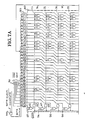
- the embodiment of Figure 5 employs a checksum register 30 comprised of a plurality of memory cells, each having a data input, a data output and a clock input for receiving a byte clock signal. Upon receipt of the byte clock signal, any data on the inputs of the memory cells will be latched into the cell and reflected on the data outputs of the cells. Each memory cell operates independently of the adjacent cells on its left and right.
- the checksum register is segmented logically into a plurality of bytes of CRC data designated bytes 0 through 3 in Figure 5. In the preferred embodiment, there are 8 bits per byte and 32 bits total in the checksum register with byte 3 being the most significant byte.
- byte 3 is comprised of memory cells 24 through 31.
- the data outputs of the checksum register are coupled to the inputs of an array of shifting links 60 as shown in Figure 7.
- This array of shifting links is comprised of one row of shifting links for each bit of an raw input data byte comprised of the data bits D0 through D7 which enter the array on the left.
- These raw input data bits are the data bits of the message upon which a CRC calculation is desired.
- Each raw input data bit is coupled to one input of an input gate.
- the designated raw input data bit is D7 and the designated input gate is the exclusive-OR gate 62.
- the designated raw input data bit is D6, and the designated input gate is the exclusive-OR gate 64.
- Each input gate has another input coupled to one of the data outputs of one of the bits of the most significant CRC byte.
- the input gate for the first row, gate 62 has its other input coupled to the data output of the most significant CRC bit, bit 31.
- the input gate for the second row has its other input coupled to the second most significant CRC bit, bit 30 and so on for all the rows.
- Each row of shifting links is comprised of a plurality of straight through conductors which do nothing but shift the bits at their inputs to their outputs which are connected to the inputs of the next row of shifting links in the next most significant bit position. That is these straight through conductors do nothing but shift their input bits one bit position left.
- the balance of the shifting links in each row are exclusive-OR gates which have one input as a bit input for the CRC bits from the checksum register or from the preceding row and which have another input coupled to the output of the input gate designated for that row. This latter input is not coupled directly to the output of the input gate, but is coupled to the output of an AND gate designated for the particular row.
- One input of this AND gate is coupled to the output of the exclusive-OR gate and another input is for receipt of a SHIFT not signal the purpose of which will be explained below.
- the output of the AND gate for each row is also coupled to the input of the least significant shifting link of the next row.
- each exclusive-OR gate shifting link is coupled to the input of the next most significant bit position shifting link in the next row, i.e., each exclusive-OR gate shifts its input bit one bit position to the left after performing the exclusive-OR operation on it.
- the relative positions of the exclusive-OR gate shifting links depends upon the particular generator polynomial being used.
- the exclusive-OR gates must be located so as to have their inputs coupled to bits 0, 1, 3, 4, 6, 7, 9, 10, 11, 15, 21, 22, 25 and 31 of the checksum register 30. The reason for this is well known to those skilled in the art of CRC calculation and will not be explained here for brevity and simplicity.
- Each row has its exclusive-OR gates in the same bit position. The inputs of the first row are coupled to the outputs of the checksum register as if it were a preceding row, and the outputs of the last row are coupled to the inputs of the checksum register as if it were the next row.
- the data outputs of the most significant byte of the CRC register are also coupled to the individual conductors of the CRC output bus 70.
- each memory cell will have a complement output, and it is these outputs of the most significant byte which are coupled to the output bus 70.
- an inverter can be used in each line to invert the CRC bits prior to transmission.
- the purpose of the AND gates and the SHIFT not signal is to allow the array of shifting links to be made transparent so that data at the output of the checksum register will pass through the array unchanged and be shifted left by one byte in the process and re-input into the checksum register.
- the SHIFT not signal is asserted, i.e., logic 0, all the AND gates such as the gates 66 and 68 have logic 0 outputs.
- the logic 0's on the lines 72 through 79 renders the exclusive-OR gates in the rows of shifting links transparent such that they pass their input data from the preceding row through to their outputs coupled to the next row without change.
- each row shifts its input data one bit to the left, and because there are 8 rows, the result is that for every cycle of the byte clock signal the data in the checksum register is shifted left by one byte when the SHIFT not signal is asserted. This allows all bytes of the CRC data to be accessed through the single byte wide output bus 70.
- the embodiment of Figure 5 may also be used in a serial format with some modifications. If the array of shifting links 84 is a single row of shifting links, then the AND gates of Figure 7 will not work to cause single byte left shifts for every byte clock signal. In a serial data input environment, the raw data input to the array 84 would be one bit at a time in serial format in synchronization with a bit clock signal. After all the raw input data bits are processed, the CRC checkbits for the message would reside in the checksum register 30. The most significant byte could be read immediately on the output bus 70.
- the remaining bytes would be shifted left one bit at time by an additional coupling of each CRC bit data output to the input of the next most significant CRC bit input, i.e., the input of the neighboring cell on the left.
- This coupling would be through a multiplexer for each bit which would have one input coupled to the bus 36 and the other input coupled to the CRC bit data output on the right.
- the output of the multiplexer would be connected to the data input of the left neighbor.
- An additional logic circuit would then disable the output bus 70 for 8 cycles of the bit clock signal connected to the clock input of each cell in the checksum register and enable it when byte 2 had been shifted into the byte 3 or most significant byte position. The same process would be performed for each byte until all bytes had been read out.
- FIG. 6 there is shown another embodiment for an output bus structure for a CRC calculation machine.
- This embodiment uses a multiplexer having 4 inputs each of which is coupled by a byte wide bus to the complement data outputs of one group of memory cells storing one byte of CRC data.
- a CRC not byte select signal on a bus 74 selects which of the four inputs to couple to the 8 bit output bus 70.
- CRC calculation is performed as described above, and it does not matter with respect to outputting the CRC data whether the array of shifting links 84 is a serial array or a parallel array or whether a bit clock or byte clock signal is used to clock the data in except the type of array and clock signal must be consistent.
- Figures 8 through 12 illustrate various embodiments for performing the preset function in two different ways and in both the serial and parallel calculation environment.
- Figure 8 shows an embodiment of a CRC calculation machine using preset apparatus which must be actuated at least one clock cycle before the first clock cycle of the CRC calculation.
- the CRC apparatus is comprised of a checksum register 30 having its data outputs coupled to the data inputs of an exclusive-OR and shift array 84 as in the embodiments described above.
- the array 84 can be serial as the array 32 of Figures 1 and 2 or it can be parallel as is the array 60 of Figures 4 or 7.
- the last row in the array is coupled through a multiplexer 86 to the data inputs of the checksum register 30 by a data bus 36 which is 32 bits wide.
- the multiplexer 86 has three 32 bit wide inputs marked A, B and C, and a 32 bit wide output bus 88 which is coupled to the data inputs of said checksum register.
- the multiplexer has three select inputs for receiving input select signals.
- the particular select signal which is active at any particular time causes its corresponding one of inputs A through C to be coupled to the output bus 88.
- the A input is 32 logic 1's
- the B input is the 32 data outputs of the checksum register collectively referred to as bus 90.
- the C input is the 32 bit bus 36 carrying the data outputs from the last row in the array 84.
- the input select signal PRESET SELECT is activated one or more clock cycles before the first clock cycle of the CRC calculation. This causes 32 logic 1's from input bus A to be coupled to the the bus 88 and loaded into the cells of the checksum register 30.
- the COMPUTE SELECT input is asserted to couple the C input or bus 36 to the bus 88. While this condition exits, CRC calculation will proceed as the data of the message for which check bits are to be generated is clocked into the array 84. If at any time it is desired to stop the CRC calculation, the HOLD SELECT input may be asserted thereby connecting the outputs of the checksum register back into the inputs via the buses 90 and 88.
- FIG 9 through 12 illustrate various embodiments of a CRC calculation machine where the preset apparatus allows the preset logic 1's to be loaded during the first clock cycle of the CRC calculation.
- These AND gates perform a logical AND operation between the clock signal and a COMPUTE signal which is asserted as a logic 1 when it is desired to compute CRC checkbits.
- COMPUTE is of logic 1
- CRC calculation can proceed.
- COMPUTE is a logic zero, no CRC computation occurs, and the contents of the checksum register are constant.
- Figures 9 and 10 show serial array and parallel array embodiments respectively using OR gates to implement the preset function.
- Figures 11 and 12 show serial and parallel array embodiments respectively using multiplexers to implement the preset function.
- Figure 10 is the preferred embodiment. All of these embodiments will be discussed simultaneously as to the preset apparatus since the elements and the operation of the various elements and the form of the CRC calculation is the same for all the embodiments. These elements operate in the same manner as in the serial and parallel array embodiments of other aspects of the invention discussed above. Further, the arrays themselves can be any of the serial or parallel arrays described herein for purposes of practicing the aspects of the invention regarding preset during the first clock cycle of the CRC calculation without adversely affecting operation of this aspect of the invention.
- each of the four OR gates 90 through 93 represents 8 OR gates, and each performs on OR logic function on the bits of one of the bytes of CRC data stored in the checksum register 30.
- Each of the 8 OR gates represented by each of the gates 90-93 has an input coupled to one of the data outputs of a memory cell in the particular group of cells in the checksum register coupled to the corresponding OR gate 90-93.
- the output of each OR gate is coupled to an input of one of the shifting links in the first row of the array.
- Each OR gate has another input coupled to a NEW PRESET signal. When this signal is asserted as a logic 1, all the outputs of the OR gates assume a logic 1 value thereby forcing logic 1's at the inputs of the array of shifting links during the first clock cycle of the CRC calculation.
- the NEW PRESET signal reverts back to the logic 0 state thereby rendering the OR gates transparent. Thereafter any data in the checksum register is transmitted through the OR gates 90 through 93 without change, and the CRC calculation proceeds normally.
- Figures 11 and 12 accomplish the same forcing of logic 1's into the inputs of the first row of the array of shifting links using multiplexers 94 through 97 to redirect the inputs of the first row of shifting links in the array 32 or 60 to a source of 32 logic 1's.
- the multiplexers 94 through 97 could be represented as one multiplexers having two 32 bit inputs. One input would be connected to each of the 32 data outputs of the cells in the checksum register 30, and the other input would be for coupling to a source of 32 logic 1's such as a voltage source coupled to each of the conductors of the input.
- the output of the multiplexer would be a 32 bit bus coupled to the data inputs of the first row of shifting links in the array.
- the multiplexer would have an input for receiving a NEW PRESET SELECT signal. This signal is asserted during the first clock cycle of the CRC calculation and causes the multiplexer to select the input coupled to the source of logic 1's and to couple these logic 1's to the inputs of the first row of shifting links in the array. After the first clock cycle of the CRC calculation, the NEW PRESET SELECT signal reverts back to the state wherein the multiplexer couples the data outputs of the checksum register 30 to the data inputs of the array. Thereafter CRC calculation proceeds normally.
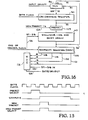
- Figure 13 shows a timing diagram showing the relationships of the clock signal and all the control signals of the embodiments of Figures 8 through 12. This diagram is self explanatory given the above discussion of the relationships of the preset signals to the first clock cycle of the CRC calcualation.
- header packets are used. These header packets are bits which define the addressed node for which the data packet attached to the header packet is intended. Such message organization is commonly used in networking of computers, terminals and peripherals.
- Figure 14A is a symbolic drawing of a typical message organization where CRCH 101 is a collection of CRC checkbits calculated on the header bits 100 and where CRCD 103 is a collection of CRC checkbits calculated on the data message 102.
- the first way is shown in Figure 14A where the CRCD checkbits are calculated on the data message 102 alone.
- the second way is shown in Figure 14B where the CRCD checkbits are calculated on the entire packet including the header 100, the CRCH checkbits 101 and the data bits 102. It is useful to have a CRC calculation machine which is capable of calculating separate CRCH and CRCD checkbit packets in either of the two ways.
- any of the embodiments described above or to be described below which have a gate in the feedback bus 36 or which have the hold bus such as the bus 91 from the output of the checksum register 30 to its input through an input multiplexer 86 can calculate separate CRCH and CRCD checkbit packets according to the method of Figure 14A. This is done by stopping the CRC calculation after the header packet has been processed, outputting the then existing contents of the checksum register 30 as the CRCH packet and then presetting the checksum register and allowing the CRC calculation to begin again when the data message 102 begins to arrive.
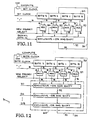
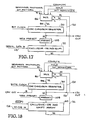
- the embodiment of Figure 15 is one embodiment of a CRC calculation machine which can compute separate CRCH and CRCD checkbit packets in accordance with the method of Figure 14B using a serial format array 32 of shifting links.
- the embodiment of Figure 16 is one embodiment of a CRC calculation machine which can compute separate CRCH and CRCD checkbit packets in accordance with the method of Figure 14B using a parallel format array 32 of shifting links. Both of these embodiments use a separate snapshot register 106 and a multiplexer 108 to implement the method of Figure 14B. The common portions of these embodiments will be described below without distinguishing between whether a serial or parallel array of shifting links is used since this is irrelevant to the operation of this aspect of the invention.
- a checksum register 30 identical in construction, operation and purpose to the checksum registers described above in other embodiments has its data inputs coupled to the data outputs of an input multiplexer 86 by a 32 bit wide bus 88.
- the multiplexer 86 has three inputs which are the same inputs and which serve the same purpose of the inputs for the multiplexer 86 in Figure 8 discussed above.
- the output of the checksum register 30 is coupled to the input of the array of shifting links either directly as in Figure 15 or through a preset means 109 as shown in Figure 16.
- the embodiment of Figure 15 uses the preset method where the logic 1's are loaded into the checksum register 30 during the clock cycle before the CRC calculation starts. This is done by asserting the INPUT SELECT signal so as to select the input C of the multiplexer 86 during the clock cycle before the start of the CRC calculation so as to load 32 logic 1's into the checksum register 30.
- the embodiment of Figure 16 uses the preset method of forcing logic 1's into the input of the array of shifting links during the first clock cycle of the CRC calculation method as described above with respect to Figures 9 through 12.
- the preset means 109 can be either OR gates like the OR gates 90 through 93 in Figures 9 and 10, or multiplexers like the multiplexers 94 through 97 shown in Figures 11 and 12. Either preset method and apparatus may be used on either of the embodiments of Figures 15 or 16.
- the array of shifting links 32 or 60 can be any of the arrays of shifting links described herein. Regardless of whether the array 32 or 60 is for processing of serial format data messages or parallel format data messages, the outputs of the array are coupled to 32 data inputs of a snapshot register 106 which serves as a storage location for a copy of the CRCH checkbits.
- the snapshot register is comprised of a plurality of memory cells like those used in the checksum register, but those skilled in the art will appreciate other types of memory cells which may be used.
- the clock inputs of the memory cells in the snapshot register 106 are for coupling to an END OF HEADER clock signal which serves to load the output of the array of shifting links 32 or 60 into the snapshot register 106 after all the header bits have been processed and the output of the array on the bus 36 consists of the CRCH bits.
- These CRCH bits can be output on the CRCH output bus 110 byte by byte by use of a multiplexer such as the multiplexer 72 in Figure 6 or in other methods which will be apparent to those skilled in the art.
- the CRCH bits must be fed back into the array of shifting links as raw input data so that CRC bits may calculated on the CRCH bits.
- This is the purpose of the multiplexer 108 and the circuitry connected to it. The structure of this circuitry will be described briefly here followed by a description of its operation in implementing the method of Figure 14A and in implementing the method of Figure 14B.
- the snapshot register 106 is connected as a shift register so that the CRCH bits may be shifted into one input of the multiplexer 108 in serial fashion on a line 112.
- the other input of the multiplexer 108 is coupled to the source of the serial raw input data.
- a select signal on a line 114 causes the multiplexer 108 to couple either the raw data in the message on line 116 or the CRCH data on the line 112 into the raw data input 118 of the array 32.
- snapshot register 106 has 4 one byte wide output buses 118 through 121 which are coupled to 4 input ports of a multiplexer 116.
- the parallel format input data bits D7 through D0 are coupled by a bus 122 to an input port of the multiplexer 116, and a BYTE SELECT signal on a line 124 controls which of the inputs of the multiplexer 116 are to be coupled to the raw data input 126 of the array of shifting links.
- Figures 15 and 16 can be used to calculate the CRCD checkbits in the manner of Figure 14A.
- a preset operation must be done. Specifically as to the Figure 15 embodiment, by asserting the INPUT SELECT signal to select input C, 32 logic 1's will be loaded into the checksum register 30 in preparation for the CRC calculation.
- the Figure 16 embodiment can perform the preset in the same manner if the input multiplexer 86 is modified in Figure 16 to have the inputs of Figure 15, and the preset operation will be performed in the same manner. Either of the Figure 15 or Figure 16 embodiments can be preset using the new preset means 109 by asserting the NEW PRESET signal on the line 126 in the manner previously described.
- CRC calculation can begin. The input A will be selected during CRC calculation on the header bits 100.
- the input B will be selected during the clock cycles when the CRCH bits are output from the checksum register 30.
- This output process for outputting CRCH can be by any of the methods described above for serial or parallel shifting arrays depending upon the type of output bus structure coupled to the snapshot register.
- the checksum register is preset to all 1's again if the method of Figure 14A is to be performed.
- the raw input data of the data message 102 is then input to the array 32 or 60 and processed to calculate the CRCD checkbits.
- the presetting steps and calculation steps are the same as above for calculating CRCH.
- they upon completion of calculation of the CRCH checkbits, they must be copied into the snapshot register 106 so that they may be output while simultaneously being fed back into the raw data input of the array of shifting links.
- the END OF HEADER signal is asserted, which causes the CRCH bits to be loaded into the snapshot register 106.
- the END OF HEADER clock signal can be the clock signal supplied to the checksum register, i.e., the BIT CLOCK signal, gated through a gate which only allow it to pass when the end of the header is detected.
- the multiplexer 116 is caused by the SELECT signal on the line 114 to couple the serial data stream on the line 112 to the raw data input 118.
- the CRCH checkbits are input to the array and operated upon in the fashion described previously.
- the multiplexer 108 is caused by the SELECT signal to switch its output 118 back to the data message bits 102 on the line 117.
- the CRCD checkbits will reside in the checksum register 30 and can be output in any of the manners described above.
- each embodiment uses an input multiplexer 86 having its data outputs coupled to the 32 data inputs of the checksum register 30 by a bus 88.
- Each multiplexer 36 has an A input coupled to the feedback bus 36 coupled to the output of the array of shifting links 32 or 60.
- Each multiplexer also has an input C coupled by a bus 130 to the data outputs of the checksum register 30.
- each multiplexer 86 has a B input coupled to a remainder polynomial bit pattern. This bit pattern represents the coefficients of the standard remainder polynomial which results when CRC checkbits are calculated on a data message and its checkbits starting from a preset state of all logic 1's.
- the arrays of shifting links can be any of the array structures described herein.
- the output of the array of shifting links is coupled to the input of the checksum register 30 through the input multiplexer 86 by the feedback bus 36.
- the input of the arrays 32 or 60 are coupled to the data outputs of the checksum register 30 through a preset means 109 which has the same structure, operation and purpose as the preset means previously described.
- the data outputs of the checksum register 30 are also coupled to an output bus 132 which can have any of the structures and and be used in any of the manners described above to output CRC data from the checksum register.
- FIGURE 14A METHOD
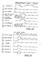
- the arrays of shifting links in the embodiments of Figures 17 and 18 are preset to all logic 1's by asserting the NEW PRESET signal during the same clock cycle that the first bit or byte of the header packet arrives as shown on time line 2 of Figure 19.
- the input select signal OLD PRESET is asserted to select the input of the input multiplexer which is coupled to a source of 32 logic one's.
- the COMPUTE input select signal is asserted causing the input A to be selected and the CRCH checkbits are calculated on the header bits.
- the CRCH checkbits will reside in the checksum register and may be shifted out on the CRC output bus in the case of the embodiment of Figure 17 or may be output one byte at a time using the apparatus described earlier herein. This process is symbolized by the assertion of the signal MUX or SHIFT on time line 4 of Figure 19. In alternative embodiments, all 32 bits of CRCH checkbits may be output in parallel.
- the input multiplexer 86 is caused by the assertion of the HOLD signal illustrated on time line 6 to select input C for coupling to the checksum register input. This maintains the contents of the checksum register constant during the time the CRCH bits are being output to implement the method of Figure 14A.
- the checksum register Upon completion of the output of the CRCH bits, the checksum register is again preset with all 1's by either asserting the NEW PRESET signal as shown on time line 7 of Figure 19 or by asserting the OLD PRESET signal during the clock cycle before the data message starts as shown on time line 8 of Figure 19. Thereafter, the input multiplexer is caused by assertion of the COMPUTE signal to again select the A input for coupling to the input of the checksum register 30. This causes the CRC calculation to resume on the raw input data bits of the data message 102 arriving at the raw data inputs 118 and 126. After all the data bits in the message 102 have been processed, the CRCD checkbits will be present in the checksum register 30. That concludes the method of calculation of the CRCH and CRCD checkbits per the method of Figure 14A.
- FIGURE 14B METHOD
- the embodiments of Figures 17 and 18 are operated as follows.
- the NEW PRESET signal is asserted during the first clock cycle of the header as before and as shown on time line 2 of Figure 19.
- the COMPUTE input select signal is simultaneously asserted as shown on time line 1 of Figure 19. This selects the input bus A of the input multiplexer for coupling to the input of the CRC checksum register.
- the CRCH calculation then proceeds as earlier described.
- the CRCH checkbits will be present in the checksum register after all the header bits have been processed.
- the CRCD checkbits must be calculated on the entire packet including the header 100, the CRCH bits 101 and the data packet 102.
- the input multiplexer is forced to select the input B at the end of outputting of all the CRCH bits during the clock cycle just before the first clock cycle in the input of the data portion 102 of the message 99. This is done by the assertion of the INITIATE REMAINDER signal illustrated on time line 5 of Figure 19.
- the CRCD checkbits reside in the checksum register and can be output in any of the manners described herein.
- One parallel format embodiment for calculating CRC checkbits on a variable number of bits in the first byte of the data message would be to make the first few rows of shifting links transparent. This would be done after presetting the checksum register to all logic 1's. The logic 1's are passed through to the first active row of shifting links coupled to the first bit of the raw input data to be included in the CRC calculation. However, the shifting action of the transparent rows of shifting links must be disabled to use this embodiment so that the least significant bits of the transparent rows are not filled with logic 0's as the logic 1's are shifted left in the transparent rows. This embodiment is more difficult to implement than the embodiment to be described next.
- One important aspect of the invention is to provide a flexible means whereby one or more bits in the first byte of a message upon which calculation of CRC bits is desired may be ignored.
- the problem in a parallel format calculation using a byte clock where several initial bits are to be ignored is to preset the appropriate row of shifting links to all 1's.
- the appropriate row is the row which has as an input to its input gate (such as the gate 62 in Figure 7) the first data bit in the raw input data of the first byte in the message which is to be included in the CRC calculation.
- Figure 20 illustrates the apparatus to accomplish this function along with the apparatus implementing the other important functions of the invention.
- variable bit boundary function is implemented by the OR gates 110 through 125.
- OR gates 110 through 125 The manner in which these OR gates cause the rows of shifting links coupled to the bits to be ignored to become transparent is best illustrated by example.
- Figure 21 is a timing diagram of the control signals needed to implement the variable bit boundary function.
- the control signals needed to control the other apparatus illustrated in Figure 20 to perform the other functions of the invention which the embodiment of Figure 20 is capable of performing are as previously described herein.
- the CALCULATE control signal for the input multiplexer 86 is asserted to select input A to allow the CRC calculation to begin as illustrated on time line 3.
- the NEW PRESET signal is asserted to force all logic 1's into the data inputs of the first row of shifting links coupled to the input data bit D7 through the input gate 62 as illustrated on the time line 2.
- the IGNORE 7, IGNORE 6 and IGNORE 5 signals are asserted.
- logic 1's will exist on the lines 132, 134 and 136.
- the input gates 62, 64 and 65 thus receive two logic 1's at their inputs because the preset gates 138, 140 and 142 are forcing their outputs to logic 1's by virtue of the logic 1 state of the NEW PRESET signal. This is true regardless of the contents of the checksum register 30 at this time.
- the output lines of the exclusive-OR gates 62, 64 and 65 will be logic 0's therefore during the first clock cycle of the CRC calculation.
- the preset gates 109 are forcing all the data inputs of the first row of shifting links to which they are connected to a logic 1 state.
- the common input line 150 of the first row also carries the input data bit for the least significant bit position shifting link of the second row. Since this bit must also be a logic 1 for the arrangement to work properly, another OR gate 118 is interposed between the common line 150 and the data input of the least significant bit position shifting link in the second row.
- This OR gate 118 has one input coupled to the common input line 150 and another input coupled to the line carrying the IGNORE 7 signal. The output of this OR gate is coupled to the input of the least significant bit position shifting link of the second row of shifting links. Since the IGNORE 7 signal is a logic 1 during the first clock cycle of the CRC calculation, a one will be forced into the input of the least significant bit position shifting link of the second row.
- Each row of shifting links in the array has an OR gate like the gate 118.
- the outputs of all these OR gates, i.e., the gates 119 through 125 is coupled to the input of the least significant bit position shifting link in the next row and each gate has one input coupled to the IGNORE signal for the row and another input coupled to the common input line for that row.
- any number of rows can have logic 1's forced into their least significant bit position shifting links by asserting the IGNORE signal for that row.
- any number of rows can be made transparent by asserting the IGNORE signal coupled to the OR gates 110 through 117 having their outputs coupled to the inputs of the input gate for the row to be made transparent.
- the IGNORE 7 through IGNORE 5 signals are asserted during the first clock cycle of the CRC calculation as shown on time lines 5 through 7 of Figure 21.
- This causes the first three rows of the array 60 to be transparent and to pass all logic 1's to the data inputs of the fourth row of shifting links.
- CRC checkbits will be calculated on all the bits of the first input byte D7 through D0 except the data bits D7 through D5. This occurs because the preset 1's are transmitted directly through the rows of shifting links coupled to the data bits D7 through D5 and so the row of shifting links coupled to data bit D4 acts like it is the first row in the array.
- the IGNORE 7 through IGNORE 5 signals are deactivated, and the CRC calculation proceeds normally.
Priority Applications (1)
| Application Number | Priority Date | Filing Date | Title |
|---|---|---|---|
| AT86309177T ATE97276T1 (de) | 1985-12-02 | 1986-11-25 | Crc-rechenmaschinen. |
Applications Claiming Priority (2)
| Application Number | Priority Date | Filing Date | Title |
|---|---|---|---|
| US803367 | 1985-12-02 | ||
| US06/803,367 US4712215A (en) | 1985-12-02 | 1985-12-02 | CRC calculation machine for separate calculation of checkbits for the header packet and data packet |
Publications (3)
| Publication Number | Publication Date |
|---|---|
| EP0230730A2 true EP0230730A2 (fr) | 1987-08-05 |
| EP0230730A3 EP0230730A3 (en) | 1990-03-14 |
| EP0230730B1 EP0230730B1 (fr) | 1993-11-10 |
Family
ID=25186354
Family Applications (1)
| Application Number | Title | Priority Date | Filing Date |
|---|---|---|---|
| EP86309177A Expired - Lifetime EP0230730B1 (fr) | 1985-12-02 | 1986-11-25 | Machines pour calculer les CRC |
Country Status (6)
| Country | Link |
|---|---|
| US (1) | US4712215A (fr) |
| EP (1) | EP0230730B1 (fr) |
| JP (1) | JPH0831802B2 (fr) |
| AT (1) | ATE97276T1 (fr) |
| DE (1) | DE3689285T2 (fr) |
| ES (1) | ES2046172T3 (fr) |
Cited By (9)
| Publication number | Priority date | Publication date | Assignee | Title |
|---|---|---|---|---|
| EP0411110A1 (fr) * | 1989-02-16 | 1991-02-06 | Grumman Aerospace Corporation | Reseau de detection d'erreurs ultrapide |
| EP0443753A1 (fr) * | 1990-02-14 | 1991-08-28 | Hewlett-Packard Company | Procédé et dispositif de production des signatures indépendantes de l'ordre pour la détection d'erreur |
| EP0495642A2 (fr) * | 1991-01-16 | 1992-07-22 | Xilinx, Inc. | Circuit et méthode pour la détection d'erreurs |
| AU627642B2 (en) * | 1990-02-06 | 1992-08-27 | Digital Equipment International Limited | Method and apparatus for generating a 48-bit framecheck sequence |
| EP0582749A1 (fr) * | 1992-07-14 | 1994-02-16 | ALCATEL BELL Naamloze Vennootschap | Dispositif de détection et de correction d'erreur |
| US5367479A (en) * | 1992-07-14 | 1994-11-22 | Alcatel N.V. | Divider device to divide a first polynomial by a second one |
| EP0631703A1 (fr) * | 1992-12-29 | 1995-01-04 | Codex Corporation | Dispositif et procede efficaces de generation et verification des coefficients de restes du controle de redondance cyclique |
| FR2722897A1 (fr) * | 1994-07-07 | 1996-01-26 | Nippon Denso Co | Microprocesseur dans lequel est incorporee une section de controle par redondance cyclique (crc) et procede pour executer des operations crc en l'utilisant |
| WO1996008874A1 (fr) * | 1994-09-16 | 1996-03-21 | Cirrus Logic, Inc. | Systeme verificateur a code detecteur d'erreur/controle de redondance cyclique |
Families Citing this family (31)
| Publication number | Priority date | Publication date | Assignee | Title |
|---|---|---|---|---|
| US4897835A (en) * | 1985-11-27 | 1990-01-30 | At&E Corporation | High capacity protocol with multistation capability |
| US5682148A (en) * | 1985-11-27 | 1997-10-28 | Seiko Corporation | Paging system with message numbering prior to transmission |
| US4901316A (en) * | 1986-05-27 | 1990-02-13 | Nohmi Bosai Kogyo Co., Ltd. | Disaster prevention monitoring and control facility |
| JPH0193933A (ja) * | 1987-10-06 | 1989-04-12 | Sony Corp | エラー訂正符号化装置 |
| US4947484A (en) * | 1987-11-10 | 1990-08-07 | Echelon Systems Corporation | Protocol for network having a plurality of intelligent cells |
| DE3890947C2 (de) * | 1987-11-10 | 1995-05-18 | Echelon Systems | Netzwerk und Verfahren zur Nachrichtenübertragung |
| US4996690A (en) * | 1988-08-26 | 1991-02-26 | Stac Electronics | Write operation with gating capability |
| GB9314479D0 (en) * | 1992-11-06 | 1993-08-25 | Hewlett Packard Co | Encoding data |
| US5390196A (en) * | 1992-11-12 | 1995-02-14 | Bull Hn Information Systems Inc. | Byte-wise determination of a checksum from a CRC-32 polynomial |
| SE470544B (sv) * | 1992-11-24 | 1994-07-25 | Ellemtel Utvecklings Ab | För en bitfelsövervakning i en väljarutrustning avsedd anordning |
| EP0614294A1 (fr) * | 1993-03-03 | 1994-09-07 | International Business Machines Corporation | Procédé pour la génération d'une séquence de test |
| FR2759796B1 (fr) * | 1997-02-19 | 2001-12-07 | Bull Sa | Dispositif et procede de detection d'erreurs sur un circuit integre comportant un port parallele serie |
| US5951707A (en) * | 1997-06-27 | 1999-09-14 | International Business Machines Corporation | Method of partitioning CRC calculation for a low-cost ATM adapter |
| US6075774A (en) * | 1997-11-18 | 2000-06-13 | 3Com Corporation | Method and device for generating a frame check sequence |
| US6681203B1 (en) * | 1999-02-26 | 2004-01-20 | Lucent Technologies Inc. | Coupled error code protection for multi-mode vocoders |
| US6320501B1 (en) | 1999-05-25 | 2001-11-20 | Pittway Corporation | Multiple sensor system for alarm determination with device-to-device communications |
| US6681364B1 (en) | 1999-09-24 | 2004-01-20 | International Business Machines Corporation | Cyclic redundancy check for partitioned frames |
| US6530061B1 (en) * | 1999-12-23 | 2003-03-04 | Intel Corporation | Method and apparatus for offloading checksum |
| US6848072B1 (en) * | 2000-09-19 | 2005-01-25 | Bbn Solutions Llc | Network processor having cyclic redundancy check implemented in hardware |
| US6643821B2 (en) * | 2000-11-30 | 2003-11-04 | Stmicroelectronics, Inc. | Method and device for computing incremental checksums |
| US20040015771A1 (en) * | 2002-07-16 | 2004-01-22 | Menahem Lasser | Error correction for non-volatile memory |
| US7607070B2 (en) * | 2004-09-13 | 2009-10-20 | National Instruments Corporation | System and method for in-line consistency checking of packetized data |
| US20060253768A1 (en) * | 2005-05-03 | 2006-11-09 | Intel Corporation | Techniques to speculatively determine network protocol unit integrity |
| DE102005029515A1 (de) * | 2005-06-25 | 2006-12-28 | Bosch Rexroth Aktiengesellschaft | Verfahren zur Berechnung von CRC-Prüfwerten und Logikschaltung |
| KR101224591B1 (ko) * | 2006-02-23 | 2013-01-22 | 삼성전자주식회사 | 네트워크 중계 장치 및 그 방법 |
| GB0607976D0 (en) * | 2006-04-22 | 2006-05-31 | Univ Belfast | Apparatus and method for computing an error detection code |
| US7823043B2 (en) * | 2006-05-10 | 2010-10-26 | Sandisk Il Ltd. | Corruption-resistant data porting with multiple error correction schemes |
| US8234539B2 (en) * | 2007-12-06 | 2012-07-31 | Sandisk Il Ltd. | Correction of errors in a memory array |
| US9891985B1 (en) * | 2014-11-01 | 2018-02-13 | Netronome Systems, Inc. | 256-bit parallel parser and checksum circuit with 1-hot state information bus |
| TWI698750B (zh) * | 2018-03-20 | 2020-07-11 | 慧榮科技股份有限公司 | 存取快閃記憶體模組的方法及相關的快閃記憶體控制器與電子裝置 |
| TWI658364B (zh) | 2018-03-20 | 2019-05-01 | 慧榮科技股份有限公司 | 存取快閃記憶體模組的方法及相關的快閃記憶體控制器與電子裝置 |
Citations (8)
| Publication number | Priority date | Publication date | Assignee | Title |
|---|---|---|---|---|
| US3703705A (en) * | 1970-12-31 | 1972-11-21 | Ibm | Multi-channel shift register |
| US3798597A (en) * | 1972-06-26 | 1974-03-19 | Honeywell Inf Systems | System and method for effecting cyclic redundancy checking |
| DE2347317A1 (de) * | 1973-09-20 | 1975-04-03 | Licentia Gmbh | Schaltungsanordnung zur erzeugung von pruefstellen in anlagen zur gesicherten datenuebertragung |
| US3893078A (en) * | 1973-04-13 | 1975-07-01 | Honeywell Inf Systems | Method and apparatus for calculating the cyclic code of a binary message |
| WO1980002611A1 (fr) * | 1979-05-15 | 1980-11-27 | Ericsson Telefon Ab L M | Prosede et dispositif de supervision de fautes lors de la transmission de donnees entre ordinateurs |
| US4380029A (en) * | 1981-03-13 | 1983-04-12 | Bti Computer Systems | Data recording format and method and apparatus for producing same |
| US4454600A (en) * | 1982-08-25 | 1984-06-12 | Ael Microtel Limited | Parallel cyclic redundancy checking circuit |
| JPS59177705A (ja) * | 1983-03-25 | 1984-10-08 | Fujitsu Ltd | デ−タ記録方式 |
Family Cites Families (10)
| Publication number | Priority date | Publication date | Assignee | Title |
|---|---|---|---|---|
| US3872430A (en) * | 1973-11-23 | 1975-03-18 | Paul Emile Boudreau | Method and apparatus of error detection for variable length words using a polynomial code |
| JPS5425764A (en) * | 1977-07-28 | 1979-02-26 | Daifuku Machinery Works | Device for simultaneous measurement of volume and weight |
| JPS5437460A (en) * | 1977-07-28 | 1979-03-19 | Chino Works Ltd | Integral ad converter |
| US4282551A (en) * | 1979-04-11 | 1981-08-04 | Hitachi, Ltd. | PCM Recording and reproducing apparatus |
| US4410989A (en) * | 1980-12-11 | 1983-10-18 | Cyclotomics, Inc. | Bit serial encoder |
| DE3122381A1 (de) * | 1981-06-05 | 1982-12-23 | Ibm Deutschland Gmbh, 7000 Stuttgart | Verfahren und einrichtung zur erzeugung von pruefbits zur sicherung eines datenwortes |
| JPS58206254A (ja) * | 1982-05-27 | 1983-12-01 | Nec Corp | 誤り検出符号生成/検査方式 |
| US4498174A (en) * | 1982-08-25 | 1985-02-05 | Ael Microtel Limited | Parallel cyclic redundancy checking circuit |
| US4593393A (en) * | 1984-02-06 | 1986-06-03 | Motorola, Inc. | Quasi parallel cyclic redundancy checker |
| JPS60206227A (ja) * | 1984-03-30 | 1985-10-17 | Oki Electric Ind Co Ltd | 誤り訂正復号回路 |
-
1985
- 1985-12-02 US US06/803,367 patent/US4712215A/en not_active Expired - Lifetime
-
1986
- 1986-11-25 AT AT86309177T patent/ATE97276T1/de not_active IP Right Cessation
- 1986-11-25 ES ES198686309177T patent/ES2046172T3/es not_active Expired - Lifetime
- 1986-11-25 DE DE86309177T patent/DE3689285T2/de not_active Expired - Fee Related
- 1986-11-25 EP EP86309177A patent/EP0230730B1/fr not_active Expired - Lifetime
- 1986-12-01 JP JP61286556A patent/JPH0831802B2/ja not_active Expired - Lifetime
Patent Citations (8)
| Publication number | Priority date | Publication date | Assignee | Title |
|---|---|---|---|---|
| US3703705A (en) * | 1970-12-31 | 1972-11-21 | Ibm | Multi-channel shift register |
| US3798597A (en) * | 1972-06-26 | 1974-03-19 | Honeywell Inf Systems | System and method for effecting cyclic redundancy checking |
| US3893078A (en) * | 1973-04-13 | 1975-07-01 | Honeywell Inf Systems | Method and apparatus for calculating the cyclic code of a binary message |
| DE2347317A1 (de) * | 1973-09-20 | 1975-04-03 | Licentia Gmbh | Schaltungsanordnung zur erzeugung von pruefstellen in anlagen zur gesicherten datenuebertragung |
| WO1980002611A1 (fr) * | 1979-05-15 | 1980-11-27 | Ericsson Telefon Ab L M | Prosede et dispositif de supervision de fautes lors de la transmission de donnees entre ordinateurs |
| US4380029A (en) * | 1981-03-13 | 1983-04-12 | Bti Computer Systems | Data recording format and method and apparatus for producing same |
| US4454600A (en) * | 1982-08-25 | 1984-06-12 | Ael Microtel Limited | Parallel cyclic redundancy checking circuit |
| JPS59177705A (ja) * | 1983-03-25 | 1984-10-08 | Fujitsu Ltd | デ−タ記録方式 |
Non-Patent Citations (4)
| Title |
|---|
| COMPUTER DESIGN. vol. 11, no. 5, May 1972, LITTLETON, MASSACHUS pages 95 - 98; PAUL KRAEGER: "SMALL COMPUTER CYCLIC REDUNDANCY CHECKSUM CAPABILITY" * |
| COMPUTER DESIGN. vol. 14, no. 10, October 1975, LITTLETON, MASSACHUS pages 102 - 106; HUGH C. McKEE: "IMPROVED CRC TECHNIQUE DETECTS ERRONEOUS LEADING AND TRAILING 0's IN TRANSMITTED DATA BLOCKS" * |
| IEEE JOURNAL OF SOLID-STATE CIRCUITS. vol. SC-15, no. 1, February 1980, NEW YORK US pages 52 - 60; ALAN J. WEISSBERGER: "AN LSI IMPLEMENTATION OF AN INTELLIGENT CRC COMPUTER AND PROGRAMMABLE CHARACTER COMPARATOR" * |
| PATENT ABSTRACTS OF JAPAN vol. 9, no. 33 (P-334)(1756) 13 February 1985, & JP-A-59 177705 (FUJITSU K.K.) 08 October 1984, * |
Cited By (16)
| Publication number | Priority date | Publication date | Assignee | Title |
|---|---|---|---|---|
| EP0411110A4 (en) * | 1989-02-16 | 1993-02-24 | Grumman Aerospace Corporation | Very high speed error detection network |
| EP0411110A1 (fr) * | 1989-02-16 | 1991-02-06 | Grumman Aerospace Corporation | Reseau de detection d'erreurs ultrapide |
| AU627642B2 (en) * | 1990-02-06 | 1992-08-27 | Digital Equipment International Limited | Method and apparatus for generating a 48-bit framecheck sequence |
| EP0443753A1 (fr) * | 1990-02-14 | 1991-08-28 | Hewlett-Packard Company | Procédé et dispositif de production des signatures indépendantes de l'ordre pour la détection d'erreur |
| US5598424A (en) * | 1991-01-16 | 1997-01-28 | Xilinx, Inc. | Error detection structure and method for serial or parallel data stream using partial polynomial check |
| EP0495642A2 (fr) * | 1991-01-16 | 1992-07-22 | Xilinx, Inc. | Circuit et méthode pour la détection d'erreurs |
| EP0495642A3 (en) * | 1991-01-16 | 1994-07-20 | Xilinx Inc | Error detection circuit and method |
| EP0582749A1 (fr) * | 1992-07-14 | 1994-02-16 | ALCATEL BELL Naamloze Vennootschap | Dispositif de détection et de correction d'erreur |
| US5367479A (en) * | 1992-07-14 | 1994-11-22 | Alcatel N.V. | Divider device to divide a first polynomial by a second one |
| US5402429A (en) * | 1992-07-14 | 1995-03-28 | Alcatel N.V. | Error detection and correction device to detect and correct single bit errors in a transmitted sequence of bits |
| EP0631703A1 (fr) * | 1992-12-29 | 1995-01-04 | Codex Corporation | Dispositif et procede efficaces de generation et verification des coefficients de restes du controle de redondance cyclique |
| EP0631703A4 (fr) * | 1992-12-29 | 1996-03-20 | Codex Corp | Dispositif et procede efficaces de generation et verification des coefficients de restes du controle de redondance cyclique. |
| FR2722897A1 (fr) * | 1994-07-07 | 1996-01-26 | Nippon Denso Co | Microprocesseur dans lequel est incorporee une section de controle par redondance cyclique (crc) et procede pour executer des operations crc en l'utilisant |
| US6195779B1 (en) | 1994-07-07 | 2001-02-27 | Denso Corporation | Microprocessor having built-in CRC section and method for performing CRC operations using the same |
| WO1996008874A1 (fr) * | 1994-09-16 | 1996-03-21 | Cirrus Logic, Inc. | Systeme verificateur a code detecteur d'erreur/controle de redondance cyclique |
| US5592498A (en) * | 1994-09-16 | 1997-01-07 | Cirrus Logic, Inc. | CRC/EDC checker system |
Also Published As
| Publication number | Publication date |
|---|---|
| JPH0831802B2 (ja) | 1996-03-27 |
| US4712215A (en) | 1987-12-08 |
| ATE97276T1 (de) | 1993-11-15 |
| DE3689285D1 (de) | 1993-12-16 |
| DE3689285T2 (de) | 1994-05-11 |
| EP0230730A3 (en) | 1990-03-14 |
| JPS62133825A (ja) | 1987-06-17 |
| EP0230730B1 (fr) | 1993-11-10 |
| ES2046172T3 (es) | 1994-02-01 |
Similar Documents
| Publication | Publication Date | Title |
|---|---|---|
| EP0230730B1 (fr) | Machines pour calculer les CRC | |
| EP0225761B1 (fr) | Appareil et procédé pour calculer des codes cycliques redondants | |
| EP0226353B1 (fr) | Appareil pour calculer des CRC | |
| US4720831A (en) | CRC calculation machine with concurrent preset and CRC calculation function | |
| US6530057B1 (en) | High speed generation and checking of cyclic redundancy check values | |
| US5321704A (en) | Error detection structure and method using partial polynomial check | |
| EP0609595B1 (fr) | Méthode et appareil pour vérifier des codes CRC par combinaison de codes cycliques partiels | |
| US4809273A (en) | Device for verifying operation of a checking code generator | |
| US7590916B2 (en) | Cyclic redundancy checking value calculator | |
| KR20050110646A (ko) | 가변 폭의 병렬 순환 중복 검사 (crc) 연산을 위한 반복회로 및 방법 | |
| KR20070006764A (ko) | 폴트 허용한계 및 증가된 안정성을 제공하는 데이터 통신모듈 | |
| US4979173A (en) | Burst mode error detection and definition | |
| US4691319A (en) | Method and system for detecting a predetermined number of unidirectional errors | |
| US10763895B2 (en) | Circuitry and method for dual mode reed-solomon-forward error correction decoder | |
| US4498178A (en) | Data error correction circuit | |
| US5140595A (en) | Burst mode error detection and definition | |
| KR950009690B1 (ko) | 순환 여유검사(crc) 동기 장치 | |
| EP0262944A2 (fr) | Appareil de correction d'erreurs | |
| EP0431416A2 (fr) | Appareil et méthode pour la réalisation d'un code de vérification d'erreur cyclique en parallèle | |
| JP3217993B2 (ja) | パリティチェック回路 | |
| US6981206B1 (en) | Method and apparatus for generating parity values | |
| US7138930B1 (en) | Multiple byte data path encoding/decoding device and method | |
| JP2591113B2 (ja) | ハミング符号化器 | |
| JP2619412B2 (ja) | 符号装置および復号装置 | |
| JP3578690B2 (ja) | 可変周期カウンタおよび位相変動追従型分離回路 |
Legal Events
| Date | Code | Title | Description |
|---|---|---|---|
| PUAI | Public reference made under article 153(3) epc to a published international application that has entered the european phase |
Free format text: ORIGINAL CODE: 0009012 |
|
| AK | Designated contracting states |
Kind code of ref document: A2 Designated state(s): AT BE CH DE ES FR GB GR IT LI LU NL SE |
|
| PUAL | Search report despatched |
Free format text: ORIGINAL CODE: 0009013 |
|
| AK | Designated contracting states |
Kind code of ref document: A3 Designated state(s): AT BE CH DE ES FR GB GR IT LI LU NL SE |
|
| 17P | Request for examination filed |
Effective date: 19900426 |
|
| 17Q | First examination report despatched |
Effective date: 19910627 |
|
| GRAA | (expected) grant |
Free format text: ORIGINAL CODE: 0009210 |
|
| AK | Designated contracting states |
Kind code of ref document: B1 Designated state(s): AT BE CH DE ES FR GB GR IT LI LU NL SE |
|
| REF | Corresponds to: |
Ref document number: 97276 Country of ref document: AT Date of ref document: 19931115 Kind code of ref document: T |
|
| REF | Corresponds to: |
Ref document number: 3689285 Country of ref document: DE Date of ref document: 19931216 |
|
| EPTA | Lu: last paid annual fee | ||
| ITF | It: translation for a ep patent filed |
Owner name: ING. C. GREGORJ S.P.A. |
|
| REG | Reference to a national code |
Ref country code: GR Ref legal event code: FG4A Free format text: 3009710 |
|
| REG | Reference to a national code |
Ref country code: ES Ref legal event code: FG2A Ref document number: 2046172 Country of ref document: ES Kind code of ref document: T3 |
|
| ET | Fr: translation filed | ||
| PLBE | No opposition filed within time limit |
Free format text: ORIGINAL CODE: 0009261 |
|
| STAA | Information on the status of an ep patent application or granted ep patent |
Free format text: STATUS: NO OPPOSITION FILED WITHIN TIME LIMIT |
|
| 26N | No opposition filed | ||
| EAL | Se: european patent in force in sweden |
Ref document number: 86309177.3 |
|
| PGFP | Annual fee paid to national office [announced via postgrant information from national office to epo] |
Ref country code: LU Payment date: 19951001 Year of fee payment: 10 |
|
| PGFP | Annual fee paid to national office [announced via postgrant information from national office to epo] |
Ref country code: SE Payment date: 19951013 Year of fee payment: 10 Ref country code: GR Payment date: 19951013 Year of fee payment: 10 |
|
| PG25 | Lapsed in a contracting state [announced via postgrant information from national office to epo] |
Ref country code: LU Free format text: LAPSE BECAUSE OF NON-PAYMENT OF DUE FEES Effective date: 19961125 |
|
| PG25 | Lapsed in a contracting state [announced via postgrant information from national office to epo] |
Ref country code: SE Effective date: 19961126 |
|
| PG25 | Lapsed in a contracting state [announced via postgrant information from national office to epo] |
Ref country code: GR Free format text: THE PATENT HAS BEEN ANNULLED BY A DECISION OF A NATIONAL AUTHORITY Effective date: 19970531 |
|
| REG | Reference to a national code |
Ref country code: GR Ref legal event code: MM2A Free format text: 3009710 |
|
| EUG | Se: european patent has lapsed |
Ref document number: 86309177.3 |
|
| PGFP | Annual fee paid to national office [announced via postgrant information from national office to epo] |
Ref country code: AT Payment date: 19971007 Year of fee payment: 12 |
|
| PGFP | Annual fee paid to national office [announced via postgrant information from national office to epo] |
Ref country code: BE Payment date: 19971211 Year of fee payment: 12 |
|
| PGFP | Annual fee paid to national office [announced via postgrant information from national office to epo] |
Ref country code: CH Payment date: 19980109 Year of fee payment: 12 |
|
| PG25 | Lapsed in a contracting state [announced via postgrant information from national office to epo] |
Ref country code: AT Free format text: LAPSE BECAUSE OF NON-PAYMENT OF DUE FEES Effective date: 19981125 |
|
| PG25 | Lapsed in a contracting state [announced via postgrant information from national office to epo] |
Ref country code: LI Free format text: LAPSE BECAUSE OF NON-PAYMENT OF DUE FEES Effective date: 19981130 Ref country code: CH Free format text: LAPSE BECAUSE OF NON-PAYMENT OF DUE FEES Effective date: 19981130 Ref country code: BE Free format text: LAPSE BECAUSE OF NON-PAYMENT OF DUE FEES Effective date: 19981130 |
|
| BERE | Be: lapsed |
Owner name: ADVANCED MICRO DEVICES INC. Effective date: 19981130 |
|
| REG | Reference to a national code |
Ref country code: CH Ref legal event code: PL |
|
| PGFP | Annual fee paid to national office [announced via postgrant information from national office to epo] |
Ref country code: ES Payment date: 19991116 Year of fee payment: 14 |
|
| PG25 | Lapsed in a contracting state [announced via postgrant information from national office to epo] |
Ref country code: ES Free format text: LAPSE BECAUSE OF NON-PAYMENT OF DUE FEES Effective date: 20001126 |
|
| REG | Reference to a national code |
Ref country code: GB Ref legal event code: IF02 |
|
| PGFP | Annual fee paid to national office [announced via postgrant information from national office to epo] |
Ref country code: GB Payment date: 20021002 Year of fee payment: 17 |
|
| PGFP | Annual fee paid to national office [announced via postgrant information from national office to epo] |
Ref country code: NL Payment date: 20021011 Year of fee payment: 17 |
|
| PGFP | Annual fee paid to national office [announced via postgrant information from national office to epo] |
Ref country code: FR Payment date: 20021105 Year of fee payment: 17 |
|
| PGFP | Annual fee paid to national office [announced via postgrant information from national office to epo] |
Ref country code: DE Payment date: 20021127 Year of fee payment: 17 |
|
| PG25 | Lapsed in a contracting state [announced via postgrant information from national office to epo] |
Ref country code: GB Free format text: LAPSE BECAUSE OF NON-PAYMENT OF DUE FEES Effective date: 20031125 |
|
| REG | Reference to a national code |
Ref country code: ES Ref legal event code: FD2A Effective date: 20011214 |
|
| PG25 | Lapsed in a contracting state [announced via postgrant information from national office to epo] |
Ref country code: NL Free format text: LAPSE BECAUSE OF NON-PAYMENT OF DUE FEES Effective date: 20040601 |
|
| PG25 | Lapsed in a contracting state [announced via postgrant information from national office to epo] |
Ref country code: DE Free format text: LAPSE BECAUSE OF NON-PAYMENT OF DUE FEES Effective date: 20040602 |
|
| GBPC | Gb: european patent ceased through non-payment of renewal fee |
Effective date: 20031125 |
|
| PG25 | Lapsed in a contracting state [announced via postgrant information from national office to epo] |
Ref country code: FR Free format text: LAPSE BECAUSE OF NON-PAYMENT OF DUE FEES Effective date: 20040730 |
|
| NLV4 | Nl: lapsed or anulled due to non-payment of the annual fee |
Effective date: 20040601 |
|
| REG | Reference to a national code |
Ref country code: FR Ref legal event code: ST |
|
| PG25 | Lapsed in a contracting state [announced via postgrant information from national office to epo] |
Ref country code: IT Free format text: LAPSE BECAUSE OF NON-PAYMENT OF DUE FEES;WARNING: LAPSES OF ITALIAN PATENTS WITH EFFECTIVE DATE BEFORE 2007 MAY HAVE OCCURRED AT ANY TIME BEFORE 2007. THE CORRECT EFFECTIVE DATE MAY BE DIFFERENT FROM THE ONE RECORDED. Effective date: 20051125 |