EP0225720A2 - Circuits intégrés - Google Patents
Circuits intégrés Download PDFInfo
- Publication number
- EP0225720A2 EP0225720A2 EP86308590A EP86308590A EP0225720A2 EP 0225720 A2 EP0225720 A2 EP 0225720A2 EP 86308590 A EP86308590 A EP 86308590A EP 86308590 A EP86308590 A EP 86308590A EP 0225720 A2 EP0225720 A2 EP 0225720A2
- Authority
- EP
- European Patent Office
- Prior art keywords
- terminal
- data
- signal
- line type
- signal processor
- Prior art date
- Legal status (The legal status is an assumption and is not a legal conclusion. Google has not performed a legal analysis and makes no representation as to the accuracy of the status listed.)
- Granted
Links
Images


Classifications
-
- G—PHYSICS
- G06—COMPUTING; CALCULATING OR COUNTING
- G06F—ELECTRIC DIGITAL DATA PROCESSING
- G06F13/00—Interconnection of, or transfer of information or other signals between, memories, input/output devices or central processing units
-
- G—PHYSICS
- G06—COMPUTING; CALCULATING OR COUNTING
- G06F—ELECTRIC DIGITAL DATA PROCESSING
- G06F13/00—Interconnection of, or transfer of information or other signals between, memories, input/output devices or central processing units
- G06F13/38—Information transfer, e.g. on bus
- G06F13/42—Bus transfer protocol, e.g. handshake; Synchronisation
- G06F13/4282—Bus transfer protocol, e.g. handshake; Synchronisation on a serial bus, e.g. I2C bus, SPI bus
- G06F13/4291—Bus transfer protocol, e.g. handshake; Synchronisation on a serial bus, e.g. I2C bus, SPI bus using a clocked protocol
Definitions
- This invention relates to integrated circuit (IC) devices.
- Most video and audio equipment (such as, for example, television receivers, video tape recorders (VTRs) and tape recorders) which have a digital circuit employ an inner bus system, for example as shown in Figure 1 of the accompanying drawings, in which a main central processing unit (CPU) 1 and a plurality of IC devices 2 1 ,2 2 Vietnamese bus line 3, and the IC devices 2 1 ,2 2 ?? 2 n are connected to control circuits 4 1 ,4 2 , ?? 4 m .
- the IC devices 2 1 to 2 n fetch predetermined data from data supplied by the CPU 1, convert the fetched data from digital to analog form, and use the resulting analog signals to control the circuits 4 1 to 4 m .
- the IC devices 2 1 to 2 n receive analog operation voltages from the circuits 4 1 to 4 m , convert the voltages from analog to digital form, and supply the resulting digital signals to the CPU 1.
- the IC devices 2 1 to 2 n function as a slave CPU.
- a read only memory (ROM) 5 stores set values of the operation voltages of the circuits 4 1 to 4 m .
- data representing a set value is read from the ROM 5 by the CPU 1 and supplied to the IC devices 2 to 2 n through the bus 3, so that the circuits 4 1 and 4 m are controlled to perform predetermined operations while a display unit 6 provides a suitable display, for example an indication that such operations are being performed.
- the circuits 4 1 to 4 m are also externally controllable by manual actuation of a keyboard 7, or by a remote control system, through the CPU 1.
- the CPU 1 and the IC devices 2 1 ,2 2 , ?? 2 n are connected in common through three lines 8 1 ,8 2 , and 8 3 .
- Chip select terminals CS 1 ,CS 2 , ?? CS n of the CPU 1 and chip select terminals CS 11 ,CS 12 , across CS 1n of the IC devices 2 1 ,2 2 , ?? 2 n are connected to each other through lines 9 1 ,9 2 , Across 9 n , respectively.
- the CPU 1 When the CPU 1 selectively communicates with the IC device 2 1 , it supplies a chip select signal of a low ("L") level from the terminal CS 1 to the respective terminal CS 11 , and a signal of a high ("H") level from the terminals CS 2 , across CS n to the terminals CS 12 , across CS 1n of the other IC devices 2 2 , ... 2 n .
- the line 8 1 transmits data from the CPU 1 to the IC devices 2 1 ,2 2 , Vietnamese 2 n
- the line 8 2 transmits data from the IC devices 2 1 ,2 2 , .
- the two-line type bus is advantageous, as compared with the four-line type bus, in that it reduces the number of wires required.
- the four-line type bus can transmit a large amount of data within a short period of time; that is, the two-line type bus has a relatively slower transmission speed. Accordingly, the four-line type bus has been used for equipment, such as a VTR, which requires complex control functions, while the two-line type bus has been used in those applications where the controlled equipment, for example a television receiver, involves relatively simple control functions.
- various predetermined circuits such as a timer circuit, a display circuit, a drive mechanism, a servo circuit, and the like, must be monitored sequentially and constantly within a one-field period of a video signal. It has been found that such monitoring and consequent control cannot be performed within a one-field period when using a two-line type bus by reason of the relatively slower transmission speed of that type of bus.
- FIG. 4A to 4C of the accompanying drawings show the data format of the signals transmitted by the two-line type bus of Figure 3, it will be seen that the line 10 1 transmits serial data D (Figure 4B) and the other line 10 2 transmits a clock signal CL ( Figure 4C).
- the data D is shown in Figure 4A as comprising a 1-bit start signal, a 7-bit address signal for designating the address assigned to one of the IC devices 2' 1 ,2' 2 , .
- a 1-bit read/write (R/W) signal for determining whether to supply data to the designated IC device or to fetch data from the designated IC device
- a 1-bit acknowledge (ACK) signal which is sent to the CPU 1' when it is confirmed that an IC device is designated and that such IC device has received data
- an 8-bit data signal representing a control level or the like
- n 9-bit data signals and a 1-bit stop signal.
- the IC devices 2 1 ,2 2 , ?? 2 used in connection with the four-line type bus of Figure 2 and the IC devices 2 ' 1 ,2' 2 , ?? 2' n used in connection with the two-line type bus of Figure 3 have different arrangements and thus generally are not compatible with each other.
- an integrated circuit (IC) device comprising:
- an integrated circuit (IC) device having a first terminal for inputting data of first and second types or formats and for outputting data, a second terminal for receiving a chip select signal, a third terminal for receiving a clock pulse signal, a fourth terminal for outputting data, first signal processing means for receiving data supplied from the first terminal and outputting data to the first terminal, second signal processing means for receiving data supplied from the first terminal and outputting data to the fourth terminal, control means for receiving data from the first or second signal processing means and outputting the data to the first terminal or to the first or second signal processing means, and means for selectively enabling one of the first and second signal processing means in accordance with the type or format of the data inputted to the first terminal.
- IC integrated circuit
- Preferred embodiments of the present invention described hereinbelow provide an IC device which can be used with both four-line and two-line type buses.
- Such an IC device can be used in a control system having a four-line type bus, wherein data having a format for a two-line type bus is transmitted, thereby allowing high-speed communication.
- such an IC device can be used in a control system using a four-line type bus, together with an IC device for a two-line type bus, so that the number of wires can be decreased.
- the preferred IC devices are compatible with input signals in formats for two-line and four-line type buses.
- the preferred IC devices are suitable for use in electronic equipment (such as, for example, television receivers, VTRs and tape recorders) having a digitally controlled internal circuit and are suitable as a CPU or a microprocessor having a communication line.
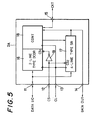
- Figure 5 shows an IC device 2A, according to a first embodiment of the present invention, which is intended for incorporation in a control system using the four-line type bus described with reference to Figure 2.
- the IC device 2A can operate even when a signal having a data format for the two-line type bus shown in Figure 4A is supplied from a main CPU 1 onto the bus.
- the IC device 2A has a data input/output terminal 11, an input terminal 12 for a chip select signal CS, an input terminal 13 for a clock pulse signal CL, a data output terminal 14, and a connection terminal 15 for connection to a circuit to be controlled, for example any of the circuits 4 1 to 4 m shown in Figure 1.
- the IC device 2A includes a decoder 16 for a signal of a two-line type bus, a shift register 17 for a signal of a four-line type bus, a controller or control unit 18, and an inverter 19.
- the chip select signal CS applied to the terminal 12 is supplied therefrom directly to a chip select terminal CS 2 of the shift register 17 and, after being inverted by the inverter 19, is applied to a chip select terminal CS of the decoder 16. Therefore, either the decoder 16 or the shift register 17 is selectively enabled by the chip select signal CS.
- the IC device 2A is operated by a signal having a data format of the two-line type bus when the signal CS is at the high ("H") level, that is, the decoder 16 is enabled in response to the signal CS being at the "H" level.
- the clock pulse signal CL applied to the terminal 13 is supplied therefrom to the decoder 16, the shift register 17, and the controller 18.
- the controller 18 generates a control signal which is outputted at the terminal 15 for controlling the controlled circuit 4 1 ?? 4m on the basis of data supplied from the decoder 16 or the shift register 17.
- the controller 18 also receives an operation voltage from the controlled circuit 4. « 4 through the terminal 15, and generates data corresponding to such operation voltage for output from the terminal 11 or for setting of such data in the shift register 17.
- the controller 18 may include a predetermined logic circuit and the like. It will be appreciated that a predetermined address is assigned to the IC device 2A.
- the decoder 16 When a signal CS of the "H" level is applied to the terminal 12, the decoder 16 is enabled, and the shift register 17 is disabled, so that the IC device 2A is placed in a two-line type mode.
- Data having a two-line type data format, as shown in Figure 4A, is supplied to the terminal 11 from the main CPU and is applied therefrom to the decoder 16 together with the clock pulse signal CL.
- the decoder 16 fetches this data when it detects the respective address at the beginning thereof.
- the controller 18 generates a control signal based on the data fetched by the decoder 16 and supplies the control signal to the controlled circuit through the terminal 15.
- the controller 18 also generates data corresponding to the operation voltage of the controlled circuit received at the terminal 16 and sends the operation voltage data to the main CPU through the terminal 11, as needed.
- the IC device 2A can be operated by a signal having the data format for a four-line type bus or a two-line type bus.
- a control system can be constituted.
- addresses are assigned to the respective IC devices so that any one of the IC devices 2A to be controlled can also be selected in the two-line type mode.
- any one of the IC devices 2A to be controlled can be selected by the chip select signal CS.
- Figure 6 shows an IC device 2B according to a second embodiment of the present invention.
- elements corresponding to those described with reference to Figure 5 are identified by the same references.
- the terminal 14 is not used in the two-line type mode so that one bus line is left unused.
- a two-line type shift register 20 is provided as the signal processor of the data in the format of a two-line type bus, and output data therefrom is applied to the terminal 14 through a two-line type gate 21. Further, output data from the shift register 17 is applied to the terminal 14 through a four-line type gate 22.
- the shift register 20 When the IC device 2B operates in the two-line type mode, the shift register 20 is enabled by the chip select signal CS at the "H" level through the inverter 19 and the shift register 17 is disabled.
- the address added to the data in the format of a two-line type bus input to the shift register 20 from the terminal 11 is compared in a comparator 23 with the address assigned to the IC device 2B.
- the controller 18 When coincidence is established in the comparator 23, the controller 18 outputs a gate signal in response to the coincidence signal.
- the gate signal enables the gate 21 and disables the gate 22 through an inverter 24. Then, the shift register 20 can send the data, received from the controller 18, to the CPU through the gate 21 and the terminal 14.
- the shift register 17 is enabled and the gates 21 and 22 are disabled and enabled, respectively, so that data outputted from the shift register 17 is supplied through the terminal 14 to the main CPU.
- the IC device 2' 2 for the two-line type bus as used in Figure 7 may be of the type described with reference to Figure 3.
- the other IC devices 2A 1 or 2B 1 may be of the kind described with reference to Figure 5 or 6.
- the IC device 2' 2 is shown connected to a data input/output line 8 1 and a clock line 8 3 , and is not connected to a data output line 8 2 . Since no chip select terminal is provided on the IC device 2' 2 , no chip select signal is supplied thereto from the CPU 1. Therefore, the IC device 2' 2 communicates with the CPU 1 when its respective identifying address is designated by the CPU 1.
- the IC device 2' 2 cannot detect that fact since chip selection is not performed with respect to the IC device 2' 2 .
- the IC device 2' 2 may erroneously output a signal at an arbitrary time when another IC device communicates with the CPU 1. If such an erroneous output signal is supplied from the IC device 2' 2 to the line 8 1 , it is mixed with a signal from another IC device which is intended to be operative, thus interfering with communication.
- a specific code for example the code "0000010” may be provided as the 7-bit address signal in the format for the data D shown in Figure 4 whenever a signal having a data format for a type of bus other than the two-line type bus is to be supplied.
- the IC device 2' 2 detects the specific address "0000010” and is made inoperative in response thereto.
- the IC device 2A or 2B is set in the four-line type mode in response to the chip selection signal CS supplied thereto after the address or code "0000010" is detected.
- an address or code other than "0000010" can be used as the specific address or code for deactivating each previously proposed or two-line type IC device included in the system of Figure 7.
- the two-line type mode is set in a step (1), and the IC device 2A or 2B awaits a start signal in a step (2).
- a check is made in a step (3) to determine whether the specific code or address "0000010" is present. If the code "0000010" is not detected in the step (3), that is the input data is in the format for a two-line type bus, the flow advances to a step (4) to check if the address of the respective IC device 2A or 2B is received. If the respective address is detected in the step (4), the IC device 2A or 2B performs a respective operation in the two-line type mode in a step (5).
- a stop signal is detected in a step (6), the communication ends and the flow returns to the step (1).
- step (3) If the special address or code "0000010" is detected in the step (3), the flow advances to a step (7) to set the IC device 2A or 2B in the four-line type mode, and then a check is made in a step (8) to determine whether chip selection is performed. If chip selection occurs in the step (8), the respective operation is performed in the four-line type mode in a step (9). Then, a check is made in a step (10) to determine whether a stop signal is detected. If a stop signal is detected in the step (10), the communication ends and the flow returns to the step (1).
Landscapes
- Engineering & Computer Science (AREA)
- Theoretical Computer Science (AREA)
- Physics & Mathematics (AREA)
- General Engineering & Computer Science (AREA)
- General Physics & Mathematics (AREA)
- Information Transfer Systems (AREA)
Applications Claiming Priority (2)
| Application Number | Priority Date | Filing Date | Title |
|---|---|---|---|
| JP60247551A JPH071496B2 (ja) | 1985-11-05 | 1985-11-05 | 制御方法及び制御装置 |
| JP247551/85 | 1985-11-05 |
Publications (3)
| Publication Number | Publication Date |
|---|---|
| EP0225720A2 true EP0225720A2 (fr) | 1987-06-16 |
| EP0225720A3 EP0225720A3 (en) | 1989-07-26 |
| EP0225720B1 EP0225720B1 (fr) | 1993-02-17 |
Family
ID=17165177
Family Applications (1)
| Application Number | Title | Priority Date | Filing Date |
|---|---|---|---|
| EP86308590A Expired - Lifetime EP0225720B1 (fr) | 1985-11-05 | 1986-11-04 | Circuits intégrés |
Country Status (7)
| Country | Link |
|---|---|
| US (1) | US4769781A (fr) |
| EP (1) | EP0225720B1 (fr) |
| JP (1) | JPH071496B2 (fr) |
| KR (1) | KR950002707B1 (fr) |
| AU (1) | AU595549B2 (fr) |
| CA (1) | CA1270576A (fr) |
| DE (1) | DE3687785T2 (fr) |
Cited By (1)
| Publication number | Priority date | Publication date | Assignee | Title |
|---|---|---|---|---|
| EP0619548A1 (fr) * | 1993-04-06 | 1994-10-12 | STMicroelectronics S.r.l. | Circuit d'interface entre un bus de commande et un circuit intégré, utilisable pour deux standards de protocoles différents |
Families Citing this family (4)
| Publication number | Priority date | Publication date | Assignee | Title |
|---|---|---|---|---|
| GB2211326B (en) * | 1987-10-16 | 1991-12-11 | Hitachi Ltd | Address bus control apparatus |
| US5461718A (en) * | 1992-04-24 | 1995-10-24 | Digital Equipment Corporation | System for sequential read of memory stream buffer detecting page mode cycles availability fetching data into a selected FIFO, and sending data without aceessing memory |
| CN101436170A (zh) * | 2007-11-12 | 2009-05-20 | 鸿富锦精密工业(深圳)有限公司 | Spi设备通信电路 |
| CN109446124B (zh) * | 2018-12-11 | 2024-03-19 | 西安热工研究院有限公司 | 一种火电机组马达及电磁阀类设备驱动级结构及方法 |
Citations (1)
| Publication number | Priority date | Publication date | Assignee | Title |
|---|---|---|---|---|
| JPS57106262A (en) | 1980-10-31 | 1982-07-02 | Philips Nv | Communication system |
Family Cites Families (4)
| Publication number | Priority date | Publication date | Assignee | Title |
|---|---|---|---|---|
| US4174536A (en) * | 1977-01-21 | 1979-11-13 | Massachusetts Institute Of Technology | Digital communications controller with firmware control |
| US4309754A (en) * | 1979-07-30 | 1982-01-05 | International Business Machines Corp. | Data interface mechanism for interfacing bit-parallel data buses of different bit width |
| US4306298A (en) * | 1979-10-09 | 1981-12-15 | Texas Instruments Incorporated | Memory system for microprocessor with multiplexed address/data bus |
| US4449202A (en) * | 1981-12-04 | 1984-05-15 | Ncr Corporation | Full duplex integrated circuit communication controller |
-
1985
- 1985-11-05 JP JP60247551A patent/JPH071496B2/ja not_active Expired - Lifetime
-
1986
- 1986-10-28 AU AU64466/86A patent/AU595549B2/en not_active Ceased
- 1986-10-30 US US06/925,374 patent/US4769781A/en not_active Expired - Lifetime
- 1986-11-03 CA CA000522007A patent/CA1270576A/fr not_active Expired - Lifetime
- 1986-11-04 DE DE8686308590T patent/DE3687785T2/de not_active Expired - Fee Related
- 1986-11-04 EP EP86308590A patent/EP0225720B1/fr not_active Expired - Lifetime
- 1986-11-05 KR KR1019860009297A patent/KR950002707B1/ko not_active IP Right Cessation
Patent Citations (1)
| Publication number | Priority date | Publication date | Assignee | Title |
|---|---|---|---|---|
| JPS57106262A (en) | 1980-10-31 | 1982-07-02 | Philips Nv | Communication system |
Cited By (2)
| Publication number | Priority date | Publication date | Assignee | Title |
|---|---|---|---|---|
| EP0619548A1 (fr) * | 1993-04-06 | 1994-10-12 | STMicroelectronics S.r.l. | Circuit d'interface entre un bus de commande et un circuit intégré, utilisable pour deux standards de protocoles différents |
| US5592633A (en) * | 1993-04-06 | 1997-01-07 | Sgs-Thomson Microelectronics, S.R.L. | Integrated circuit interface to control bus with either of two different protocol standards |
Also Published As
| Publication number | Publication date |
|---|---|
| AU595549B2 (en) | 1990-04-05 |
| KR950002707B1 (ko) | 1995-03-24 |
| JPS62107357A (ja) | 1987-05-18 |
| EP0225720A3 (en) | 1989-07-26 |
| EP0225720B1 (fr) | 1993-02-17 |
| DE3687785D1 (de) | 1993-03-25 |
| KR870005303A (ko) | 1987-06-08 |
| JPH071496B2 (ja) | 1995-01-11 |
| AU6446686A (en) | 1987-05-07 |
| CA1270576A (fr) | 1990-06-19 |
| US4769781A (en) | 1988-09-06 |
| DE3687785T2 (de) | 1993-07-22 |
Similar Documents
| Publication | Publication Date | Title |
|---|---|---|
| EP0619548B1 (fr) | Circuit d'interface entre un bus de commande et un circuit intégré, utilisable pour deux standards de protocoles différents | |
| JP2597864B2 (ja) | スマート制御及びセンサデバイス付シングルワイヤバスの多重化装置 | |
| EP0456012A2 (fr) | Circuit de commande d'affichage pour réduire la consommation d'énergie | |
| US4843539A (en) | Information transfer system for transferring binary information | |
| KR940001275B1 (ko) | 기기내 버스를 이용한 동작 제어방법 | |
| EP0589499A1 (fr) | Système omnibus de communication à stations multiples ainsi que station maître et station esclave destinées à être utilisées dans un tel système | |
| US5291080A (en) | Integrated circuit device having tristate input buffer for reducing internal power use | |
| EP0225720A2 (fr) | Circuits intégrés | |
| CA2336385A1 (fr) | Protocole ameliore de bus en serie entre dispositifs | |
| US4751574A (en) | Electronic apparatus control system | |
| EP0079524B1 (fr) | Appareil endoscopique | |
| US6418349B1 (en) | Arrangement and method for the transmission of address, instruction and/or data telegrams | |
| US6192437B1 (en) | Transmission apparatus with control circuit/relay within each card providing connection to related card output depending on related slot ID/ redundancy/non-redundancy, working/protection signals | |
| GB2203578A (en) | Information monitoring control system | |
| US5786885A (en) | Image processing system | |
| JP4931727B2 (ja) | データ通信システム | |
| KR0155641B1 (ko) | 티브이 성능 검사장치와 검사방법 | |
| US6650579B1 (en) | Semiconductor device having test and read modes and protection such that ROM data reading is prevented in the test mode | |
| JP2002366505A (ja) | 実装位置検出方法及び装置 | |
| JP3228542B2 (ja) | 電源制御装置 | |
| EP0536756A1 (fr) | Micro-ordinateur et son circuit d'établissement d'options | |
| JP3288114B2 (ja) | マイクロコンピュータ | |
| JP3488250B2 (ja) | シリアルデータ通信方式 | |
| KR19980014552A (ko) | Iic버스콘트롤시스템에서의 복수ic제어방법 | |
| KR920004283B1 (ko) | 엘리베이터의 데이타 송수신방식 |
Legal Events
| Date | Code | Title | Description |
|---|---|---|---|
| PUAI | Public reference made under article 153(3) epc to a published international application that has entered the european phase |
Free format text: ORIGINAL CODE: 0009012 |
|
| AK | Designated contracting states |
Kind code of ref document: A2 Designated state(s): DE FR GB NL |
|
| PUAL | Search report despatched |
Free format text: ORIGINAL CODE: 0009013 |
|
| AK | Designated contracting states |
Kind code of ref document: A3 Designated state(s): DE FR GB NL |
|
| 17P | Request for examination filed |
Effective date: 19891229 |
|
| 17Q | First examination report despatched |
Effective date: 19910816 |
|
| GRAA | (expected) grant |
Free format text: ORIGINAL CODE: 0009210 |
|
| AK | Designated contracting states |
Kind code of ref document: B1 Designated state(s): DE FR GB NL |
|
| REF | Corresponds to: |
Ref document number: 3687785 Country of ref document: DE Date of ref document: 19930325 |
|
| ET | Fr: translation filed | ||
| PLBE | No opposition filed within time limit |
Free format text: ORIGINAL CODE: 0009261 |
|
| STAA | Information on the status of an ep patent application or granted ep patent |
Free format text: STATUS: NO OPPOSITION FILED WITHIN TIME LIMIT |
|
| 26N | No opposition filed | ||
| PGFP | Annual fee paid to national office [announced via postgrant information from national office to epo] |
Ref country code: GB Payment date: 20011107 Year of fee payment: 16 |
|
| PGFP | Annual fee paid to national office [announced via postgrant information from national office to epo] |
Ref country code: FR Payment date: 20011113 Year of fee payment: 16 |
|
| PGFP | Annual fee paid to national office [announced via postgrant information from national office to epo] |
Ref country code: DE Payment date: 20011119 Year of fee payment: 16 |
|
| PGFP | Annual fee paid to national office [announced via postgrant information from national office to epo] |
Ref country code: NL Payment date: 20011129 Year of fee payment: 16 |
|
| REG | Reference to a national code |
Ref country code: GB Ref legal event code: IF02 |
|
| PG25 | Lapsed in a contracting state [announced via postgrant information from national office to epo] |
Ref country code: GB Free format text: LAPSE BECAUSE OF NON-PAYMENT OF DUE FEES Effective date: 20021104 |
|
| PG25 | Lapsed in a contracting state [announced via postgrant information from national office to epo] |
Ref country code: NL Free format text: LAPSE BECAUSE OF NON-PAYMENT OF DUE FEES Effective date: 20030601 |
|
| PG25 | Lapsed in a contracting state [announced via postgrant information from national office to epo] |
Ref country code: DE Free format text: LAPSE BECAUSE OF NON-PAYMENT OF DUE FEES Effective date: 20030603 |
|
| GBPC | Gb: european patent ceased through non-payment of renewal fee | ||
| PG25 | Lapsed in a contracting state [announced via postgrant information from national office to epo] |
Ref country code: FR Free format text: LAPSE BECAUSE OF NON-PAYMENT OF DUE FEES Effective date: 20030731 |
|
| NLV4 | Nl: lapsed or anulled due to non-payment of the annual fee |
Effective date: 20030601 |
|
| REG | Reference to a national code |
Ref country code: FR Ref legal event code: ST |