EP0219682B1 - Strom/Spannungswandlerschaltung - Google Patents
Strom/Spannungswandlerschaltung Download PDFInfo
- Publication number
- EP0219682B1 EP0219682B1 EP86112730A EP86112730A EP0219682B1 EP 0219682 B1 EP0219682 B1 EP 0219682B1 EP 86112730 A EP86112730 A EP 86112730A EP 86112730 A EP86112730 A EP 86112730A EP 0219682 B1 EP0219682 B1 EP 0219682B1
- Authority
- EP
- European Patent Office
- Prior art keywords
- coupled
- transistor
- emitter
- collector
- current
- Prior art date
- Legal status (The legal status is an assumption and is not a legal conclusion. Google has not performed a legal analysis and makes no representation as to the accuracy of the status listed.)
- Expired
Links
- 238000006243 chemical reaction Methods 0.000 claims description 13
- 230000008878 coupling Effects 0.000 claims description 4
- 238000010168 coupling process Methods 0.000 claims description 4
- 238000005859 coupling reaction Methods 0.000 claims description 4
- 230000003139 buffering effect Effects 0.000 claims description 3
- 238000005070 sampling Methods 0.000 claims description 2
- 238000012358 sourcing Methods 0.000 claims 1
- 238000010586 diagram Methods 0.000 description 4
- 239000004020 conductor Substances 0.000 description 3
- 238000004519 manufacturing process Methods 0.000 description 3
- 238000000034 method Methods 0.000 description 3
- 238000005513 bias potential Methods 0.000 description 1
- 239000003990 capacitor Substances 0.000 description 1
- 230000000694 effects Effects 0.000 description 1
- 230000010355 oscillation Effects 0.000 description 1
Images

Classifications
-
- G—PHYSICS
- G05—CONTROLLING; REGULATING
- G05F—SYSTEMS FOR REGULATING ELECTRIC OR MAGNETIC VARIABLES
- G05F1/00—Automatic systems in which deviations of an electric quantity from one or more predetermined values are detected at the output of the system and fed back to a device within the system to restore the detected quantity to its predetermined value or values, i.e. retroactive systems
- G05F1/10—Regulating voltage or current
- G05F1/46—Regulating voltage or current wherein the variable actually regulated by the final control device is DC
- G05F1/56—Regulating voltage or current wherein the variable actually regulated by the final control device is DC using semiconductor devices in series with the load as final control devices
- G05F1/561—Voltage to current converters
-
- G—PHYSICS
- G05—CONTROLLING; REGULATING
- G05F—SYSTEMS FOR REGULATING ELECTRIC OR MAGNETIC VARIABLES
- G05F3/00—Non-retroactive systems for regulating electric variables by using an uncontrolled element, or an uncontrolled combination of elements, such element or such combination having self-regulating properties
- G05F3/02—Regulating voltage or current
- G05F3/08—Regulating voltage or current wherein the variable is DC
- G05F3/10—Regulating voltage or current wherein the variable is DC using uncontrolled devices with non-linear characteristics
- G05F3/16—Regulating voltage or current wherein the variable is DC using uncontrolled devices with non-linear characteristics being semiconductor devices
- G05F3/20—Regulating voltage or current wherein the variable is DC using uncontrolled devices with non-linear characteristics being semiconductor devices using diode- transistor combinations
- G05F3/26—Current mirrors
- G05F3/265—Current mirrors using bipolar transistors only
Definitions
- the present invention relates to converter circuits and, more particularly, to a circuit for producing an output voltage that is representative of an applied current input.
- DAC digital to analog converter
- Such a conversion circuit requires an accurate current mirror in conjunction with other circuitry for accurately converting the applied current input into the output voltage.
- a need exists for a current to voltage integrated conversion circuit including a precision current mirror in conjunction with feedback circuitry for producing an output voltage having a known relationship to an applied current input signal.
- US-A-4,485,352 discloses a current mirror with buffering and similar feedback topology
- US-A-4,525,683 features a base current error cancellation circuit.
- a current to voltage conversion circuit comprising: a current mirror circuit including first and second transistors each having a collector, a base and an emitter, said bases being coupled together; amplifier means having an input coupled to said collector of said first transistor and having an output coupled to the output of the circuit for buffering the voltage developed at said collector of said first transistor; a feedback network for sampling the voltage at the output and returning a proportional signal to said emitter of said second transistor; and current supply means for providing substantially equal currents to said collectors of said first and second transistors, the conversion circuit having an input coupled to said emitter of said first transistor via a resistor network characterized in that the balancing of the voltages developed at said collectors of said first and second transistors is achieved by coupling the inverting and noninverting inputs of a differential amplifier to said collectors of said first and second transistors, respectively, and by coupling the output of said differential amplifier to said bases of said first and second transistors.
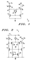
- FIG. 1 there is shown a block diagram of a precision current mirror 10 that is utilized in the conversion circuit of the present invention.
- Current mirror 10 is suited to be manufactured in integrated circuit form and can be fabricated using present day low voltage integrated circuit fabrication processes.
- Current mirror 10 includes a pair of matched, i.e. equal emitter area transistors 12 and 14 which have their base or control electrodes coupled together. The emitters or first electrodes of the transistors are returned to ground reference.
- the collector or second electrode of transistor 12 is coupled both to reference current source 16 and the non-inverting input of differential amplifier l8 at node 20.
- the inverting input of differential amplifier l8 is coupled to the collector of transistor l4 at node 22 at which an output current I O is sunk.
- the output of amplifier l8 is coupled to the bases of transistors l2 and l4.
- the output of current mirror l0 is taken at output terminal 26.
- output 26 is coupled to some load circuitry (not shown) such that the current I o is sourced from node 22 which establishes the voltage V O thereat.
- Differential or operational amplifier l8 forces the voltage developed at node 20 to be substantially equal in value to the voltage V O while providing base current drive at the output thereof to transistors l2 and l4.
- a quiescent operating balanced state is established when transistor l2 is supplied sufficient base drive to enable it to sink substantially all of the current supplied from current reference l6. Since transistors l2 and l4 are matched devices, they will have the same base-emitter voltage drop thereacross whereby the current I O will be substantially equal to the current I R .
- Differential amplifier l8 is illustrated in FIG. 2 comprises a pair of PNP transistors 28 and 30 the emitters of which are differentially connected to current supply 32. The bases of these transistors are coupled respectively to nodes 20 and 22 which correspond to the two inputs of amplifier l8.
- the collectors of transistors 28 and 30 are coupled to a differential-to-single ended output load comprising diode connected transistor 34 and transistor 36.
- the differential-to-single ended load circuit is conventional in operation and is well known to those skilled in the art.
- Current supply 32 provides the "tail" current to the differential amplifier.
- transistor 30 will be rendered conductive to supply the base currents to transistors l2 and l4 thereby turning these devices on until the balanced condition is reached at which transistor l4 sinks the current I O from the load circuitry coupled to output 26.
- transistor l2 is supplied sufficient base current drive from transistor 30 to sink all of the current from supply l6.
- Transistor 28 is sufficiently turned on by transistor l2 being rendered conductive to, in turn, render diode connected transistor 34 conductive. This turns on transistor 36 such that transistor 30 provides the required base current drive to transistors l2 and l4 as previously described. Any variations in the voltage V O established at node 22 is forced onto node 20 as aforementioned.
- the collector-base voltage drops across transistor l2 and l4 track each other whereby the operation of the current mirror l0 functions in the manner described above with reference to FIG. 1.
- FIG. 3 there is illustrated current to voltage converter circuit 40 of the present invention which includes current mirror l0 as described above.
- Converter 40 produces a voltage at output 38 that is representative of the current input supplied at input 42 to the current mirror.
- components of FIG. 3 corresponding to like components shown in FIGS. 1 and 2 are designated by the same reference numerals.
- current to voltage converter circuit 40 is suited to be fabricated in integrated circuit form using conventional bipolar fabrication processes well known to those skilled in the art of manufacturing integrated circuits.
- Current mirror l0 is realized by differential amplifier l8 which comprises transistors l2, l4, 28, 30, 34, and 36 as described above.
- the reference current supply circuit includes a pair of matched PNP transistors 44 and 46 the bases of which are coupled together with the emitter of transistor 48. The emitters of transistors 44 and 46 are returned to power supply conductor 24 via resistors 50 and 52 respectively.
- a current source 54 is coupled with the collector of transistor 44 as well as to the base of transistor 48 which sources a predetermined and substantially constant current I R to ground reference via power supply conductor 56.
- Multiple collector transistor 46 has two of its collectors coupled via diodes 60 and 62 to nodes 20 and 22, the inputs of differential amplifier l8. A third collector of transistor 46 is connected via lead 58 to supply the tail current required by differential amplifier l8 as described above.
- the emitter of transistor l2 is coupled to ground reference through series connected resistors 64 and 66.
- the emitter of transistor l4 is coupled to ground reference through series connected resistors 68 and 70 with the interconnection therebetween being connected to input 42.
- An amplifier comprising NPN transistor 72 and quasi-Darlington connected NPN transistors 74 and 76 provides both the voltage output and a current feedback signal via resistor 78 to the interconnection between resistors 64 and 66, at node 80, of current mirror l0.
- Resistor 82 provides biasing between transistor 74 and 76 as is well known.
- the base of transistor 72 is coupled to the anode of diode 60 at which is established a bias potential for the transistor.
- the input to the amplifier is coupled to the output of current mirror l0 at node 22 and corresponds to the base of transistor 74.
- Capacitor 84 stabilizes the loop formed between current mirror l0 and the amplifier by placing a pole in the transfer characteristics of converter 40 to prevent oscillations.
- converter 40 In operation, with no current input supplied at input terminal 42, converter 40 will seek a balanced operating state or condition that forces the voltage developed across resistor 66 to be equal to the voltage established across resistor 70 as will now be described.
- Transistors 44 and 46 are turned on by base current drive sourced through transistor 48 whereby current supply 54 sources a current through transistor 44 substantially equal to the value I R .
- This current is mirrored through transistor 46 such that bias currents are sourced from the multiple collectors of the transistor to render differential amplifier l8 operative.
- a bias voltage is therefore developed across diode 60 which enables transistor 72 to be turned on which, in turn, enables transistor 74 and 76 to be rendered conductive.
- Diode 62 it should be noted, is provided to ensure that current mirror l0 has a balanced configuration.
- transistors 30 and 36 are rendered less conductive than transistors l2 and 28 whereby excess current drive is available to the base of transistor 74.
- transistor 74 and 76 to conduct which supply a current feedback via resistor 78 to node 80 which raises the voltage developed across resistor 66 until this voltage equals the voltage established across resistor 70.
- transistors l2 and l4 conduct equally and the current sourced to output 22 of the current mirror l0 is equal to the current sank through transistor l4 plus the base current drive to transistor 74.
- the operation of the current to voltage converter circuit 40 is then at a quiescent balanced operating condition.
- the output voltage developed at output 38 is the sum of the voltages developed across resistors 66 and 78.
- the output voltage is proportional to the ratio of resistors 66 and 78 and is a function of the current signal applied at input 42.
- Current to voltage converter 40 may be utilized to provide a digital analog conversion. If, for example, multiple current inputs are supplied to input 42 that correspond to individual bits of a digital coded input signal, the analog output voltage produced at output 38 is representative of the digital signal.
Landscapes
- Engineering & Computer Science (AREA)
- Physics & Mathematics (AREA)
- Electromagnetism (AREA)
- General Physics & Mathematics (AREA)
- Radar, Positioning & Navigation (AREA)
- Automation & Control Theory (AREA)
- Microelectronics & Electronic Packaging (AREA)
- Nonlinear Science (AREA)
- Amplifiers (AREA)
Claims (8)
- Strom/Spannungswandlerschaltung (40), enthaltend:
eine Stromspiegelschaltung mit ersten und zweiten Transistoren (14, 12) jeweils mit Kollektor, Basis und Emitter, wobei die Basen miteinander verbunden sind;
eine Verstärkereinrichtung (72, 74, 76) mit einem Eingang, der mit dem Kollektor des ersten Transistors (14) verbunden ist und einem Ausgang, der mit dem Ausgang (38) der Schaltung (40) verbunden ist, um die an dem Kollektor des ersten Transistors (14) entwickelte Spannung zu puffern;
ein Rückkopplungsnetzwerk (78) zum Abnehmen der Spannung am Ausgang (38) und Rückführen eines proportionalen Signals zum Emitter des zweiten Transistors (12); und
eine Stromzuführungseinrichtung (46) zum Zuführen im wesentlichen gleicher Ströme zu den Kollektoren der ersten und zweiten Transistoren, wobei die Wandlerschasltung (40) einen Eingang (42) aufweist, der mit dem Emitter des ersten Transistors (14) über ein Widerstandsnetzwerk (68, 70) verbunden ist,
dadurch gekennzeichnet, daß
der Ausgleich der Spannungen, die an den Kollektoren der ersten und zweiten Transistoren ermittelt werden, durch Verbindung der invertierenden und nicht-invertierenden Eingänge eines Differenzverstärkers (18) mit den Kollektoren der ersten (14) bzw. zweiten (12) Transistoren und durch Verbinden des Ausgangs des Differenzverstärkers mit den Basen der ersten und zweiten Transistoren erzielt wird. - Schaltung nach Anspruch 1, bei der die Stromspiegelschaltung enthält:
erste (68) und zweite (70) Widerstände, die in Serie zwischen den Emitter des ersten Transistors und ein Massebezugspotential geschaltet sind, wobei der Eingang (42) der Wandlerschaltung (40) mit der Verbindung zwischen den ersten und zweiten Widerständen verbunden ist; und
dritte (64) und vierte (66) Widerstände, die in Serie zwischen den Emitter des zweiten Transistors und das Massebezugspotential geschaltet sind, wobei die Verbindung zwischen den dritten und vierten Widerständen mit dem Ausgang der Verstärkereinrichtung (72, 74, 76) verbunden ist. - Schaltung nach Anspruch 2, bei der das Rückkopplungsnetzwerk (78) einen Widerstand enthält, der zwischen den Ausgang (38) und die Verbindung der dritten und vierten Widerstände geschaltet ist.
- Schaltung nach Anspruch 3, bei der die Verstärkereinrichtung enthält:
einen dritten Transistor (74) mit einer Basis, einem Kollektor und einem Emitter, wobei der Kollektor mit einer Quelle für ein Betriebspotential verbunden ist und die Basis mit dem Ausgang der Stromspiegelschaltung verbunden ist; und
einen vierten Transistor (76) mit einer Basis, einem Kollektor und einem Emitter, wobei der Emitter mit dem Ausgang der Verstärkereinrichtung verbunden ist, der Kollektor mit der Quelle für das Betriebspotential verbunden ist und die Basis mit dem Emitter des dritten Transistors verbunden ist. - Schaltung nach Anspruch 4, bei der die Stromzuführungseinrichtung enthält:
einen fünften Transistor (44) mit eine Basis, einem Kollektor und einem Emitter, wobei der Emitter mit der Quelle für das Betriebspotential gegebenenfalls über einen Widerstand verbunden ist;
einen sechsten Transistor (46) mit einer Basis, einem Emitter und ersten und zweiten Kollektoren, wobei der Emitter mit der Quelle für das Betriebspotential gegebenenfalls über einen Widerstand verbunden ist, die ersten und zweiten Kollektoren den invertierenden bzw. nicht-invertierenden Eingängen des Differenzverstärkers verbunden sind, und die Basis mit der Basis des fünften Transistors verbunden ist; und
eine Stromquelleneinrichtung (54) zwischen dem Kollektor des fünften Transistors und dem Massebezugspotential zur Zuführung eines Bezugsstromes davon. - Schaltung nach Anspruch 5, bei der die Stromversorgungseinrichtung weiterhin einen siebenten Transistor (48) mit einer Basis, einem Kollektor und einem Emitter enthält, wobei der Emitter mit der Basis des fünften Transistors verbunden ist, der Kollektor mit dem Massebezugspotential verbunden ist und die Basis mit dem Kollektor des fünften Transistors verbunden ist.
- Schaltung nach Anspruch 6, bei der die Stromspielgeinrichtung weiterhin erste und zweite Dioden (60, 62) enthält, die zwischen die ersten bzw. zweiten Kollektoren des sechsten Transistors und den invertierenden bzw. nicht-invertierenden Eingang des Differenzverstärkers geschaltet sind.
- Schaltung nach Anspruch 7, bei der die Verstärkereinrichtung einen achten Transistor (72) mit einer Basis, einem Kollektor und einem Emitter enthält, wobei der Emitter mit dem Kollektor des dritten Transistors verbunden ist, der Kollektor mit der Quelle für das Betriebspotential verbunden ist und die Basis mit dem zweiten Kollektor des sechsten Transistors verbunden ist.
Applications Claiming Priority (2)
| Application Number | Priority Date | Filing Date | Title |
|---|---|---|---|
| US790026 | 1985-10-22 | ||
| US06/790,026 US4642551A (en) | 1985-10-22 | 1985-10-22 | Current to voltage converter circuit |
Publications (3)
| Publication Number | Publication Date |
|---|---|
| EP0219682A2 EP0219682A2 (de) | 1987-04-29 |
| EP0219682A3 EP0219682A3 (en) | 1988-08-24 |
| EP0219682B1 true EP0219682B1 (de) | 1991-11-27 |
Family
ID=25149418
Family Applications (1)
| Application Number | Title | Priority Date | Filing Date |
|---|---|---|---|
| EP86112730A Expired EP0219682B1 (de) | 1985-10-22 | 1986-09-15 | Strom/Spannungswandlerschaltung |
Country Status (5)
| Country | Link |
|---|---|
| US (1) | US4642551A (de) |
| EP (1) | EP0219682B1 (de) |
| JP (1) | JPS62100008A (de) |
| DE (1) | DE3682647D1 (de) |
| HK (1) | HK5394A (de) |
Families Citing this family (20)
| Publication number | Priority date | Publication date | Assignee | Title |
|---|---|---|---|---|
| US4706013A (en) * | 1986-11-20 | 1987-11-10 | Industrial Technology Research Institute | Matching current source |
| US4893030A (en) * | 1986-12-04 | 1990-01-09 | Western Digital Corporation | Biasing circuit for generating precise currents in an integrated circuit |
| KR900008541B1 (ko) * | 1986-12-04 | 1990-11-24 | 웨스턴 디지탈 코포레이숀 | 집적회로내에서 정밀전류(precise current)를 발생시키기 위한 바이어스 회로 |
| IT1213415B (it) * | 1986-12-17 | 1989-12-20 | Sgs Microelettronica Spa | Circuito per la misura lineare della corrente circolante su un carico. |
| US4868482A (en) * | 1987-10-05 | 1989-09-19 | Western Digital Corporation | CMOS integrated circuit having precision resistor elements |
| US4855618A (en) * | 1988-02-16 | 1989-08-08 | Analog Devices, Inc. | MOS current mirror with high output impedance and compliance |
| FR2655791A1 (fr) * | 1989-12-13 | 1991-06-14 | Siemens Automotive Sa | Circuit de miroir de courant corrige de l'effet early. |
| US5068593A (en) * | 1990-10-15 | 1991-11-26 | National Semiconductor Corporation | Piece-wise current source whose output falls as control voltage rises |
| FR2677781B1 (fr) * | 1991-06-14 | 1993-08-20 | Thomson Composants Militaires | Source de courant adaptee a des variations rapides de tension de sortie. |
| US5182462A (en) * | 1992-03-03 | 1993-01-26 | National Semiconductor Corp. | Current source whose output increases as control voltages are balanced |
| US6356065B1 (en) * | 1999-08-30 | 2002-03-12 | Canon Kabushiki Kaisha | Current-voltage converter with changeable threshold based on peak inputted current |
| US6300833B1 (en) * | 1999-12-26 | 2001-10-09 | Semiconductor Components Industries Llc | DC gain enhancement for operational amplifiers |
| DE10035414A1 (de) * | 2000-07-20 | 2002-02-07 | Infineon Technologies Ag | Integrierter Schaltkreis mit Referenzstromversorgung |
| US6778113B2 (en) * | 2002-06-03 | 2004-08-17 | Texas Instruments Incorporated | Canceling feedback resister loading effect in a shunt-shunt feedback circuit |
| DE10309877A1 (de) * | 2003-03-06 | 2004-09-16 | Infineon Technologies Ag | Transimpedanzverstärker mit hoher Verstärkungsbandbreite zum Konvertieren eines DAC-Ausgangsstroms |
| US20060055465A1 (en) * | 2004-09-15 | 2006-03-16 | Shui-Mu Lin | Low voltage output current mirror method and apparatus thereof |
| JP2006201761A (ja) * | 2004-12-21 | 2006-08-03 | Matsushita Electric Ind Co Ltd | 電流駆動装置,データドライバ,および表示装置 |
| JP5017043B2 (ja) * | 2007-09-28 | 2012-09-05 | 株式会社東芝 | 受光回路 |
| US7724092B2 (en) * | 2007-10-03 | 2010-05-25 | Qualcomm, Incorporated | Dual-path current amplifier |
| US8581659B2 (en) * | 2010-01-25 | 2013-11-12 | Dongbu Hitek Co., Ltd. | Current controlled current source, and methods of controlling a current source and/or regulating a circuit |
Family Cites Families (6)
| Publication number | Priority date | Publication date | Assignee | Title |
|---|---|---|---|---|
| DE2412393C3 (de) * | 1973-03-20 | 1979-02-08 | N.V. Philips' Gloeilampenfabrieken, Eindhoven (Niederlande) | Stromstabilisierungsschaltung |
| US4501979A (en) * | 1982-08-30 | 1985-02-26 | Motorola, Inc. | Current amplifier having multiple selectable outputs |
| US4485352A (en) * | 1982-08-30 | 1984-11-27 | Motorola, Inc. | Current amplifier |
| JPH069326B2 (ja) * | 1983-05-26 | 1994-02-02 | ソニー株式会社 | カレントミラー回路 |
| US4525683A (en) * | 1983-12-05 | 1985-06-25 | Motorola, Inc. | Current mirror having base current error cancellation circuit |
| JPH0622298B2 (ja) * | 1984-03-09 | 1994-03-23 | 松下電器産業株式会社 | 電流電圧変換装置 |
-
1985
- 1985-10-22 US US06/790,026 patent/US4642551A/en not_active Expired - Lifetime
-
1986
- 1986-09-15 EP EP86112730A patent/EP0219682B1/de not_active Expired
- 1986-09-15 DE DE8686112730T patent/DE3682647D1/de not_active Expired - Lifetime
- 1986-10-16 JP JP61244333A patent/JPS62100008A/ja active Pending
-
1994
- 1994-01-20 HK HK53/94A patent/HK5394A/en not_active IP Right Cessation
Also Published As
| Publication number | Publication date |
|---|---|
| US4642551A (en) | 1987-02-10 |
| JPS62100008A (ja) | 1987-05-09 |
| EP0219682A2 (de) | 1987-04-29 |
| EP0219682A3 (en) | 1988-08-24 |
| DE3682647D1 (de) | 1992-01-09 |
| HK5394A (en) | 1994-01-28 |
Similar Documents
| Publication | Publication Date | Title |
|---|---|---|
| EP0219682B1 (de) | Strom/Spannungswandlerschaltung | |
| US4647841A (en) | Low voltage, high precision current source | |
| GB2236444A (en) | Current mirror | |
| US5081378A (en) | Logarithmic amplifier | |
| US5729231A (en) | Digital-to-analog converter having improved resistance to variations in DC current gain | |
| JPH1022748A (ja) | 電圧電流変換回路 | |
| JPH0770935B2 (ja) | 差動電流増幅回路 | |
| EP0155717B1 (de) | Gegentakt-Verstärker | |
| EP0156410B1 (de) | Verstärkeranordnung | |
| EP0288697B1 (de) | Massstabgerechte Spannungspegelumsetzungsschaltung | |
| US6191635B1 (en) | Level shifting circuit having a fixed output common mode level | |
| US4370608A (en) | Integrable conversion circuit for converting input voltage to output current or voltage | |
| US4899064A (en) | Absolute value differential amplifier | |
| JPS6154286B2 (de) | ||
| JP2896029B2 (ja) | 電圧電流変換回路 | |
| JP3063124B2 (ja) | 増幅回路 | |
| JPH05343933A (ja) | 電圧電流変換回路 | |
| US5204638A (en) | Intrinsic offset recovery circuit particularly for amplifiers | |
| JPS6133710Y2 (de) | ||
| JPS6121857Y2 (de) | ||
| EP0205539A1 (de) | Aktives schaltungselement | |
| JPH06260925A (ja) | レベルシフト回路 | |
| JPH11177353A (ja) | 電圧電流変換回路 | |
| JPH04297121A (ja) | 比較回路 | |
| JPH0352248B2 (de) |
Legal Events
| Date | Code | Title | Description |
|---|---|---|---|
| PUAI | Public reference made under article 153(3) epc to a published international application that has entered the european phase |
Free format text: ORIGINAL CODE: 0009012 |
|
| AK | Designated contracting states |
Kind code of ref document: A2 Designated state(s): DE GB IT NL |
|
| PUAL | Search report despatched |
Free format text: ORIGINAL CODE: 0009013 |
|
| AK | Designated contracting states |
Kind code of ref document: A3 Designated state(s): DE GB IT NL |
|
| 17P | Request for examination filed |
Effective date: 19880929 |
|
| 17Q | First examination report despatched |
Effective date: 19900927 |
|
| GRAA | (expected) grant |
Free format text: ORIGINAL CODE: 0009210 |
|
| ITF | It: translation for a ep patent filed | ||
| AK | Designated contracting states |
Kind code of ref document: B1 Designated state(s): DE GB IT NL |
|
| REF | Corresponds to: |
Ref document number: 3682647 Country of ref document: DE Date of ref document: 19920109 |
|
| PLBE | No opposition filed within time limit |
Free format text: ORIGINAL CODE: 0009261 |
|
| STAA | Information on the status of an ep patent application or granted ep patent |
Free format text: STATUS: NO OPPOSITION FILED WITHIN TIME LIMIT |
|
| 26N | No opposition filed | ||
| REG | Reference to a national code |
Ref country code: GB Ref legal event code: 746 Effective date: 19990706 |
|
| REG | Reference to a national code |
Ref country code: GB Ref legal event code: IF02 |
|
| PGFP | Annual fee paid to national office [announced via postgrant information from national office to epo] |
Ref country code: NL Payment date: 20020618 Year of fee payment: 17 |
|
| PGFP | Annual fee paid to national office [announced via postgrant information from national office to epo] |
Ref country code: GB Payment date: 20020808 Year of fee payment: 17 |
|
| PGFP | Annual fee paid to national office [announced via postgrant information from national office to epo] |
Ref country code: DE Payment date: 20020930 Year of fee payment: 17 |
|
| PG25 | Lapsed in a contracting state [announced via postgrant information from national office to epo] |
Ref country code: GB Free format text: LAPSE BECAUSE OF NON-PAYMENT OF DUE FEES Effective date: 20030915 |
|
| PG25 | Lapsed in a contracting state [announced via postgrant information from national office to epo] |
Ref country code: NL Free format text: LAPSE BECAUSE OF NON-PAYMENT OF DUE FEES Effective date: 20040401 Ref country code: DE Free format text: LAPSE BECAUSE OF NON-PAYMENT OF DUE FEES Effective date: 20040401 |
|
| GBPC | Gb: european patent ceased through non-payment of renewal fee |
Effective date: 20030915 |
|
| NLV4 | Nl: lapsed or anulled due to non-payment of the annual fee |
Effective date: 20040401 |
|
| PG25 | Lapsed in a contracting state [announced via postgrant information from national office to epo] |
Ref country code: IT Free format text: LAPSE BECAUSE OF NON-PAYMENT OF DUE FEES;WARNING: LAPSES OF ITALIAN PATENTS WITH EFFECTIVE DATE BEFORE 2007 MAY HAVE OCCURRED AT ANY TIME BEFORE 2007. THE CORRECT EFFECTIVE DATE MAY BE DIFFERENT FROM THE ONE RECORDED. Effective date: 20050915 |